˲̬�������϶�Ag����ʯīϩSn-Ag-Cu���Ϻ�����淴Ӧ��Ӱ��
��Դ�ڿ����й���ɫ����ѧ��(Ӣ�İ�)2021���8��
�������ߣ������� ����� ������ ������ ����
����ҳ�룺2454 - 2467
�ؼ��ʣ�����˲̬���ϣ�Ag����ʯīϩ��Cu6Sn5������ǿ��
Key words��transient current bonding; Ag-GNS; Cu6Sn5; shear strength
ժ Ҫ��Ϊ���о�Ag����ʯīϩ��ǿ��Sn-Ag-Cu(SAC/Ag-GNSs)�����ڴ�ͳ������������Ag-GNSs���۳����ϸ��ۼ����⣬���õ����ܶ�(1.0��104 A/cm2)�ڼ��ٺ�����ʵ��Cu-SAC/Ag-GNSs-Cu��ͷ���ټ��ϡ����������Ag-GNSs���ȷ�ɢ�ں����У�ΪCu6Sn5�����ɺ��ṩ�����κ�λ�㣬�Ӷ�ϸ���������������������������Ȳ���⣬����Ag-GNSs�ľ��ȷֲ�����֯���䣬Cu6Sn5����ò�ɰ�״ת��Ϊ��״��ͬʱ��˲̬�������Ϲ��պ������ǿ�ȵ�������ߺͶ��ѻ����ı仯�����ھ��ȷֲ���Ag-GNSs�����ṹ�仯��
Abstract: To address the problem of floating and aggregation of Ag-GNSs in the molten pool during the traditional reflow soldering process, Cu/SAC/Ag-GNSs/Cu sandwich joints were prepared under an applied current density (1.0��104 A/cm2) for a few hundred milliseconds to produce Ag-coated graphene-reinforced Sn-Ag-Cu (SAC/Ag- GNSs) solder joints. The experimental results showed that Ag-GNSs were homogenously dispersed in the solder joints, providing more Cu6Sn5 grain nucleation sites, which refined these grains and reduced the thickness difference at the anode and cathode. In addition, the Cu6Sn5 morphology changed from rod-like to plate-shaped because of the uniform distribution of Ag-GNSs and constitutional supercooling. The significantly increased shear strength of the transient current bonding and the change in the fracture mechanism were due to the uniformly distributed Ag-GNSs and the microstructural changes.
Trans. Nonferrous Met. Soc. China 31(2021) 2454-2467
Yong-dian HAN1,2, Jia-hang YANG1,2, Lian-yong XU1,2, Hong-yang JING1,2, Lei ZHAO1,2
1. School of Materials Science and Engineering, Tianjin University, Tianjin 300350, China;
2. Tianjin Key Laboratory of Advanced Joining Technology, Tianjin 300350, China
Received 4 August 2020; accepted 14 January 2021
Abstract: To address the problem of floating and aggregation of Ag-GNSs in the molten pool during the traditional reflow soldering process, Cu/SAC/Ag-GNSs/Cu sandwich joints were prepared under an applied current density (1.0��104 A/cm2) for a few hundred milliseconds to produce Ag-coated graphene-reinforced Sn-Ag-Cu (SAC/Ag- GNSs) solder joints. The experimental results showed that Ag-GNSs were homogenously dispersed in the solder joints, providing more Cu6Sn5 grain nucleation sites, which refined these grains and reduced the thickness difference at the anode and cathode. In addition, the Cu6Sn5 morphology changed from rod-like to plate-shaped because of the uniform distribution of Ag-GNSs and constitutional supercooling. The significantly increased shear strength of the transient current bonding and the change in the fracture mechanism were due to the uniformly distributed Ag-GNSs and the microstructural changes.
Key words: transient current bonding; Ag-GNS; Cu6Sn5; shear strength
1 Introduction
Sn-Ag-Cu (SAC) solder has been extensively applied in the electronic industry to replace the traditional Pb-Sn solder [1-3]. Nevertheless, such solders still have disadvantages, including a high melting point, poor mechanical properties, and the overgrowth of interfacial intermetallic compounds (IMCs) [4-7]. To overcome these limitations and improve the overall properties, such as yield strength, creep resistance, thermo-mechanical fatigue resistance, electrical conductivity, and heat resistance, composite solders have been synthesized by adding different reinforcing particles to the SAC alloys [8-12]. To effectively refine IMCs and improve reliability, SHARMA et al [13] and YANG et al [14] added graphene to the SAC solder. Other researchers [15-17] have attempted to distribute graphene uniformly in solder to solve the problem of discharging from the molten solder during the reflow process. To improve the bonding between the graphene and the solder matrix, the graphene surface can be modified using second-phase metals. CHEN et al [18] made the reaction of Ni nanoparticle-modified graphene nanosheets (Ni-GNSs) with Sn to form (Ni, Cu)6Sn5 and prevented the discharge of graphene during reflow soldering. XU et al [19] modified graphene with Ag nanoparticles (Ag-GNSs) to improve the interconnection between Ag-GNSs and the Sn matrix, which enhanced the graphene grain refinement and the strengthening effect by evenly distributing the Ag-GNSs. However, owing to the low density of graphene and the long required bonding time, the graphene in the SAC solders still floats and aggregates to some extent during the reflow process.
Recently, to promote solid�Cliquid interactions and facilitate IMC formation to obtain the reliable joints, some researchers have attempted to increase the bonding temperature [20,21] or use ultrasonic- assisted connections [22,23]. The solder melting time can be reduced by shortening the bonding time. This prevents excessive floating and aggregation of graphene, thus achieving uniformly distributed graphene in the solder joints. Recently, various studies on the diffusion of Cu atoms in Cu-Sn joints under the effect of an applied current reported that electronic wind can promote the diffusion of Cu atoms in the Sn matrix through solid-liquid electromigration (EM) [24-27]. Therefore, a method for transiently bonding Cu�CSn joints through electrical effects was proposed. To achieve rapid sintering of the nanosilver paste, MEI et al [28] used the current-assisted sintering technology. TIAN et al [29-31] applied a specific current density to obtain an effective Cu/solder/Cu solder joint in a few hundred milliseconds. In addition, through electric current-assisted bonding, Cu6Sn5 can form at the Cu�Cpure Sn interface. Current researches mainly focus on the second-phase metal particles to modify GNSs to obtain excellent composite solder joints. However, for graphene- reinforced Pb-free solders, transient bonding methods to solve the problem of graphene floating during the reflow process have not been reported in-depth.
Accordingly, this study aims to fabricate Cu/ 96.5Sn-3.0Ag-0.5Cu/Ag-GNSs (SAC/Ag-GNSs)/ Cu joints in a few hundred milliseconds using electrical-effect bonding. Herein, the effects of current on graphene distribution, interfacial reactions, and the shear strength of SAC/Ag-GNS solder interconnections were investigated. The microstructures of the solder joints were characterized via scanning electron microscopy (SEM). Additionally, to evaluate the mechanical properties of the joints with transient current bonding, shear tests were performed. To demonstrate their excellent performance, the transient current bonding joints were compared with traditional reflow soldering joints.
2 Experimental
2.1 Sample preparation
In this work, solder matrix SAC/Ag-GNSs [4] was investigated. Graphene (XFNANO Material Tech Co., Ltd.) was mixed with sodium lauryl sulfate and then ultrasonically treated in dimethyl- formamide for 2 h. Subsequently, 0.06 mol/mL of silver nitrate was added to the above mixture and ultrasonicated for 30 min, and heated at 70 ��C for 1 h. Subsequently, the mixture was filtered and washed with deionized water and alcohol to prepare Ag-GNSs. The Ag-GNSs and 96.5Sn-3.0Ag- 0.5Cu solder (Shenzhen Fitech Co., Ltd.) were combined using a ball mill to obtain a mixed powder. Subsequently, the mixed powder was loaded into a mold to be press-formed and placed in a high-vacuum tube resistance furnace and sintered at 175 ��C for 2 h. Finally, the SAC/Ag-GNSs (Table 1) samples were punched using a hydraulic press.
Table 1 Chemical composition of Sn-Ag-Cu/Ag-GNSs alloy (wt.%)
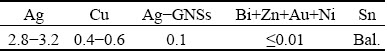
Figure 1(a) shows a schematic illustration of the Cu/solder/Cu interconnect system. The thickness and diameter of the pure Cu substrate were 1 and 5 mm, respectively. The thickness and diameter of the solder were 75 ��m and 5 mm, respectively. Before bonding, Cu was polished on both sides with a 0.5 ��m diamond and cleaned with acetone, absolute ethanol, and deionized water for 5 min. To ensure that the surface was clean and oil-free, the solder sheets were ultrasonically cleaned for 3 min in the same step. Moreover, to avoid welding instability caused by the excessive resistance of debris, the surface roughness of the Cu and solders was prepared to be as consistent as possible, and the contact surface of the electrode was formed in a uniform manner.
2.2 Bonding process
Two custom Cu-W electrodes were employed in the experimental device. The DC bonding current waveform is shown in Fig. 1(b). The Cu/solder/Cu joints were prepared over different durations (100, 150, 200, and 250 ms) at a peak bonding current of 1.96��103 A, and electron flow (labeled by ��e��) from top to bottom. Therefore, the current density through the intermediate layer of the solder sheet was 1.0��104 A/cm2, and the pressure provided by the two ends of the electrode was 0.4 MPa. Additionally, lead-free flux (LEF-100) was used in the bonding process. Furthermore, the real-time temperature of the sandwiched Cu/solder/Cu interconnect system was measured using an infrared thermal imager (InfraTec Infrared Thermometer) at a rate of 60 frame/s.
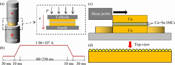
Fig. 1 Schematic illustration of Cu/solder/Cu transient current bonding interconnect system (a), bonding current waveform (b), experimental diagram of shear test (c), and schematic diagram of sample from side (d)
For comparison, Cu and solder sheets were placed on a 10 mm �� 10 mm Cu substrate and bonded using the traditional reflow method. During the reflow process, the heating rate was 1 ��C/s, maintained at 245 ��C for 1 min. Following this, the samples were cooled to room temperature in air.
2.3 Characterization and mechanical tests
A cross-section of the sample was mounted in epoxy resin, ground, and polished along the cross-sectional direction, then etched in a methanol solution containing 1 vol.% hydrochloric acid for 8 s. The microstructural evolution was observed via SEM, and the intermetallic phase was defined via EDS and XRD. As shown in Fig. 1(c), the shear tests were performed using a bonding tester (Condor 150-3 HF) at room temperature and a shear rate of 200 ��m/s. Subsequently, to remove the redundant Sn to obtain a three-dimensional shape of the solder, the shear test samples were treated by an etching solution for 15 s. After the fracture sample was deeply etched, IMC could be observed on the top view from the longitudinal direction after the fracture sample was deeply etched, and a schematic illustration is shown in Fig. 1(d).
3 Results
3.1 Bonding temperature
Figure 2 shows the temperature profiles of the solder joint center at different time (100, 150, 200, and 250 ms) and the Cu substrate boundary temperature (A: midpoint of Cu substrate interface boundary) during the transient current bonding process. From Fig. 2, it can be observed that the temperature of the solder joint rose sharply to 220 ��C (melting point of SAC/Ag-GNSs) within 70 ms and reached the peak temperature within the corresponding bonding time. Therefore, the solder of the Cu/solder/Cu intermediate layer was melted during the bonding process. During the loading duration, metallurgical reactions occurred between the solid�Cliquid Cu�Csolder, leading to the formation of different microstructures in the Cu/solder/Cu joints. When the loading time is 100, 150, 200 and 250 ms, the melting time of the solder at temperatures above 220 ��C is 100, 272, 353, and 400 ms, respectively. The corresponding peak temperatures are 260, 322, 418 and 452 ��C, respectively. The boundary of the temperature- changing curve of the electrode is similar with that of the solder joint. However, the peak temperature is 141 ��C, which is significantly lower than that of the solder joint and can reduce the impact on the substrate during the bonding process.
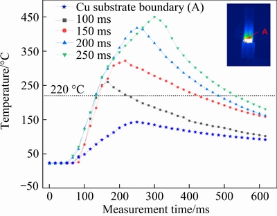
Fig. 2 Over temperature profiles at center of solder joint at 100, 150, 200, and 250 ms, and Cu substrate boundary temperature at 200 ms
3.2 Microstructural characterization
Figure 3 shows a comparison of the differences in IMC morphologies formed at the solder/Cu interface between reflow soldering and transient current bonding (100 ms). A typical shell-shaped Cu6Sn5 can be observed at the lower interface of the solder/Cu in the reflow soldering joint (Fig. 3(a)). However, a transformation occurred in the morphology of the IMCs from shell-shaped Cu6Sn5 IMCs to smoother, layered IMCs at the upper interface of the solder/Cu. The thicknesses of lower and upper interface IMCs layer were 6.28 and 4.92 ��m, respectively. In addition, it is evident from Fig. 4(a) that the C content of the upper interface of the reflow soldering joint is higher than that of the lower interface, which could indicate that the difference in the IMCs was because of the floating and agglomeration of graphene during the bonding process. In the 100 ms transient current bonding (Fig. 3(b)), it was observed that short rod-shaped IMCs were formed at the anode and the cathode solder/Cu interface, and some IMCs were distributed uniformly in the solder matrix. According to EDS results (Fig. 5), the mole fractions of Cu and Sn were 49.51% and 40.10%, respectively, which proved that the IMCs were Cu6Sn5. Notably, C appeared in the EDS spectra, which proves the presence of Ag-GNSs. Furthermore, EDS analysis was performed on the uniformly distributed Cu6Sn5 in the solder matrix. 12 points were randomly selected from the distributed Cu6Sn5 and 8 out of the 12 points distinctly exhibited the presence of Ag-GNSs. In addition, as shown in Fig. 4(b), there are no significant changes in the C content from the cathode to the anode in the current bonding joint. Therefore, from the above observations, it can be inferred that Cu6Sn5, which was uniformly distributed in the solder matrix, accompanied the Ag-GNSs in the solder matrix.
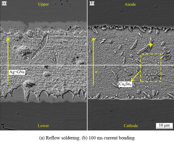
Fig. 3 Cross-sectional SEM images of IMCs
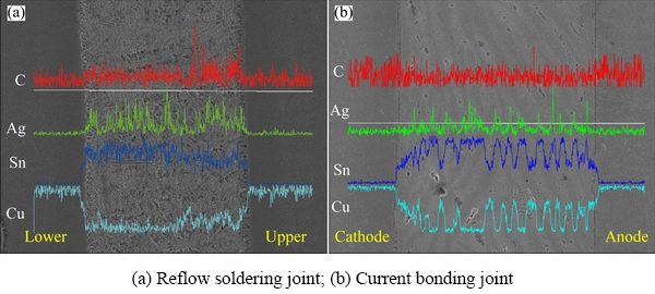
Fig. 4 EDS line scan results of ICMs
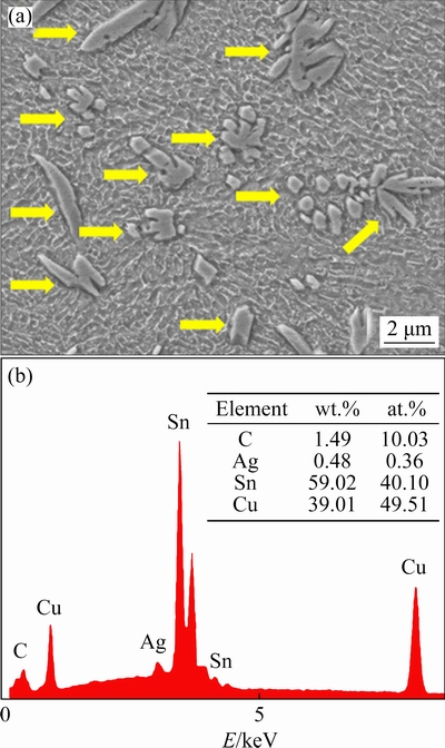
Fig. 5 High magnification SEM image of Cu6Sn5 (a) in current bonding joint and corresponding EDS result (b)
Figure 6 shows the cross-sectional SEM images and the corresponding element distribution after different bonding time. The peak temperature of the solder joint increased from 274 to 322 ��C when the bonding time increased from 100 to 150 ms, which resulted in a stronger interface reaction in the solid�Cliquid Cu�Csolder, and more Cu diffused into the liquid solder. As shown in Fig. 6(a), the IMC layer increased slightly and short rod-shaped Cu6Sn5 at the interface elongated with dendrites. Additionally, some dissociated Cu6Sn5 grains in the solder matrix fused and formed large dendrites. From the cross-sectional SEM image of Fig. 6(b), it can be observed that the morphology of the Cu6Sn5 became long rod-shaped and extended from the Cu interface to the SAC solder matrix. The IMCs at the two interfaces were coarse and long, and some of the long rod-like Cu6Sn5 were staggered in contact with each other. The Cu6Sn5 arrangement was directional when the loading time was 250 ms, which was parallel to the direction of the electron flow. The XRD results showed that the ��-Cu6Sn5 phase formed in the Cu/solder/Cu joint after different bonding time (Fig. 7). The IMC formed at the joint was the ��-Cu6Sn5 phase when the bonding time increased from 100 to 250 ms. However, the IMC content in the joint increased, and the morphology transformed from short rod- shaped to long rod-shaped type with protrusions. Furthermore, the sizes of Cu6Sn5 at the anode and cathode interfaces were similar. Additionally, two thin layers of Cu6Sn5 compounds were formed at the interface of the solid Cu and liquid solder. When the loading time is 100, 150, 200, and 250 ms, the thicknesses of the anode and cathode calculated by Image J were 0.91 and 0.98 ��m, 1.13 and 1.21 ��m, 1.86 and 2.15 ��m, and 3.67 and 4.27 ��m, respectively. The similar Cu6Sn5 morphology at the cathode and anode interfaces and the almost similar thickness of the IMC layers to that of the reflow soldering owing to the Ag-GNSs in the solder did not show floating agglomeration during transient current bonding.
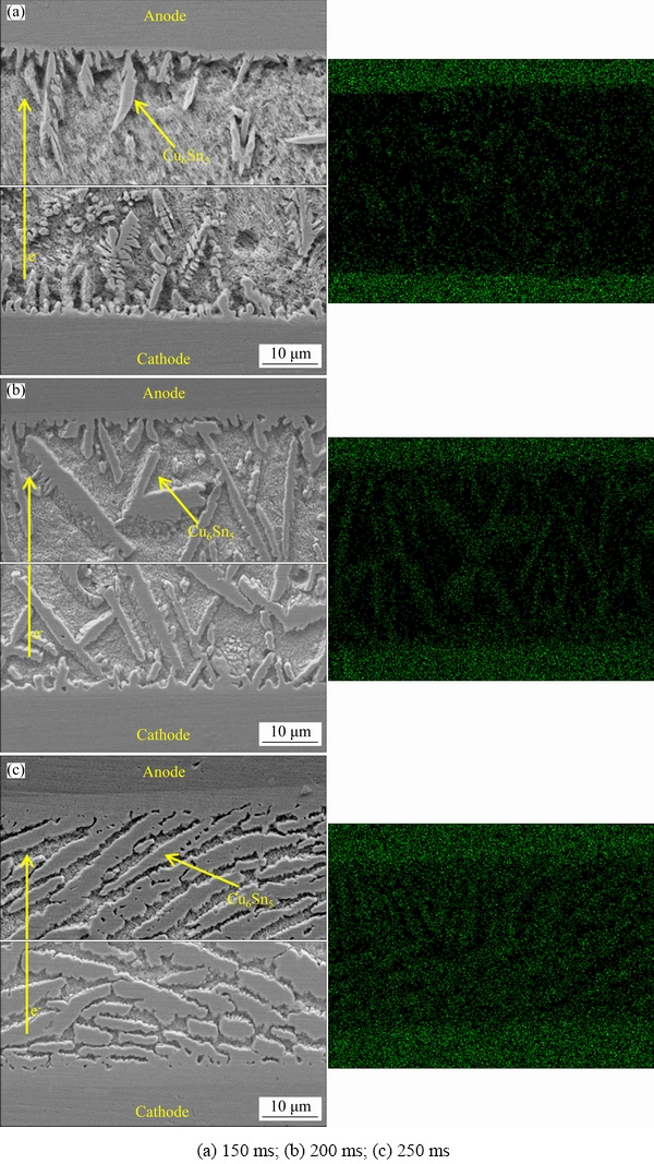
Fig. 6 Cross-sectional SEM images and corresponding Cu element distribution of joint after different bonding durations
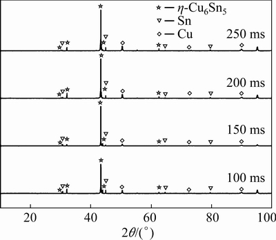
Fig. 7 XRD patterns of phase at interface after different bonding time
Figure 8 shows a top view of the morphology of the Cu6Sn5 grains at bonding time ranging from 100 to 250 ms and reflow soldering. As shown in Fig. 8(a), the interface was full of large blocks of Cu6Sn5 grains. Additionally, some voids occurred in the grains that could reduce the mechanical properties. Based on the cross-sectional SEM images, the top morphology of the Cu6Sn5 grains changed significantly at different bonding time. The morphology of the Cu6Sn5 grains after 100 ms was a short rod-like type (Fig. 8(b)). As shown in Fig. 8(c), the rod-like Cu6Sn5 grains fused, becoming small and plate-shaped at a higher peak temperature when the bonding time was 150 ms. As shown in Fig. 8(d), at 200 ms, the size of the plates increased, and there were plenty of small and intensive protrusions on the surface of the plates. When the time increased to 250 ms (Fig. 8(e)), the growth of the plate-shaped Cu6Sn5 grain was more significant. And the Cu6Sn5 grains were larger and thicker with more protrusions. As the bonding time increased, the peak temperature increased from 260 to 452 ��C through Joule heating, which caused more Cu atoms to diffuse from the Cu substrate into the SAC solder. Furthermore, an increase in time of the solid�Cliquid electromigration of Cu is a critical factor for the growth of Cu6Sn5. Cu atoms from the solid Cu and SAC matrix promoted diffusion from the cathode to the anode via EM. The ultra-fast manufacture of Cu/solder/Cu joints was mainly because of the enhanced solid�Cliquid interdiffusion kinetics. The heating effect and the Cu transformation in the molten SAC matrix by the solid�Cliquid EM lead to this phenomenon.
3.3 Shear properties
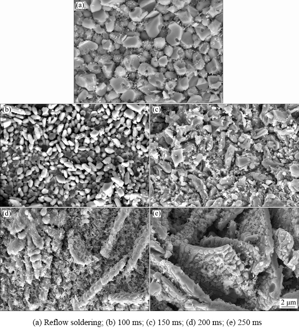
Fig. 8 Top-view morphologies of Cu6Sn5 grains
Shear strength is considered a critical parameter of mechanical performance because it is closely related to the reliability of a solder joint [7]. AHMED et al [32] reported that the factors that affect the shear strength of solder joints mainly included the microstructure, dislocation motion, chemical composition, and processing temperature. The joint composition consisted of different microstructures and proportions depending on the bonding method and loading time. The vast majority of Cu/solder/Cu joints were residual SAC matrix within the reflow soldering, 100 ms and 150 ms transient current bonding, which were regarded as SAC-base solder joints. The joints mainly consisted of flat-shaped Cu6Sn5 grains when the bonding time was increased to 200 and 250 ms; therefore, these were regarded as Cu6Sn5-based solder joints. Shear tests were performed on the bonded specimens of 100, 150, 200, and 250 ms, and the reflow soldering joints.
In Fig. 9, it can be observed that the average shear strength of the transient current bonding joints was higher than that of the reflow soldering joints. The shear strength of the reflow soldering joints (22.2 MPa) was approximately half that of the transient current bonding time joints. The SAC-based solder joint formed short rod-shaped Cu6Sn5 at the interface with uniformly distributed Cu6Sn5 in the solder layer at 100 ms. Additionally, it exhibited a robust shear strength of 39.8 MPa, which was approximately 80% higher than that of the SAC-base solder joint formed by reflow soldering. The average strength of the Cu6Sn5-based solder joint reached 55.9 and 57.7 MPa at 200 and 250 ms, respectively. Therefore, the microstructures, composition, and content of the Cu6Sn5 have a significant effect on the shear strength of the joints. These results are similar to those reported by CHOUDHURY and LADANI [33].
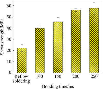
Fig. 9 Shear strength of different bonding time joints and reflow soldering joints
4 Discussion
4.1 Cu6Sn5 incubation under transient current bonding
The differences in transient bonding morphologies and reflow soldering Cu-Sn IMCs revealed that the distribution of Ag-GNSs and the flow of a strong current changed the results of the solid-liquid reaction at the Cu-Sn interface. When the current flows through the joint, the SAC solder can be melted by Joule heating in a short duration (milliseconds). Moreover, the electric current in the solid�Cliquid Cu-solder-Cu system stimulated the Cu atoms to dissolve and diffuse from the solid Cu substrate to the liquid SAC matrix. In recent research [31], Cu was seen to dissolve in the solder to form a supersaturated liquid alloy, while a Cu6Sn5 layer formed at interconnects.
As shown in Fig. 3(a), there was less disorder hindering the diffusion of Cu or Sn atoms. This formed a thicker IMC layer with a typical shell shape at the lower interface. On the contrary, a smoother IMC layer was formed at the upper interface. Furthermore, the thicknesses of the IMC layer at the lower and upper interfaces are 6.28 and 4.92 ��m respectively with a thickness variation of 21.7%. In the case of transient current bonding, it can be inferred from Fig. 3(b) that dissociative Cu6Sn5 uniformly appeared in the SAC matrix with Ag-GNSs. The thicknesses of the IMC layers were 0.91 and 0.98 ��m at anode and cathode interconnects, respectively, while the thickness change rate was 7.1%. It was reported that the energy of the Cu6Sn5 grain nucleation was provided by the surface and interface energy between the solder matrix and the IMC particles [34,35]. For the heterogeneous interface to reduce the nucleation potential barrier during the nucleation process, the interface replacement energy must be lower than the formation energy. To minimize the surface energy, various reinforcements were adsorbed on the plane, which could provide more nucleation sites. In this study, Ag-GNSs particles were embedded on the surface of the solder particles via ball milling, establishing a reliable connection. In addition, Ag-GNSs have a large and rough surface area, which reduces the critical nucleation surface energy for heterogeneous nucleation. During the bonding process, Ag-GNSs reduced the surface energy to provide more sites for Cu6Sn5 grains to nucleate in the molten solder. In the case of reflow soldering, Ag-GNSs floated upwards and aggregated at the upper interface (Fig. 10(a)). The great amount of Ag-GNSs hindered the diffusion of Cu/Sn atoms at the upper interface with a high specific surface area. Thus, the morphology of the Cu6Sn5 transformed into a planar-shape rather than a shell shape. However, in the case of transient current bonding, the floating and aggregation of Ag-GNSs during bonding can be ignored owing to the short bonding time. In addition, for the thin IMC layer to be induced at the interface of the SAC/Cu, the Cu content in the solder must be increased by the electromigration of Cu within hundreds of milliseconds. Nevertheless, Ag-GNSs hindered the diffusion of the Cu/Sn atoms in the solder matrix, which resulted in an increase in the concentration gradient of Cu near the Ag-GNSs where more Cu atoms could react with Sn to form Cu6Sn5. Therefore, because of the uniform distribution of Ag-GNSs in the solder during the bonding and solid�Cliquid EM of Cu, the uniformly distributed Cu6Sn5 and thinner interface IMC layer were rapidly formed during the 100 ms current bonding process.
4.2 Cu6Sn5 growth under transient current bonding
For conventional reflow process, the Cu6Sn5 morphology is usually shell-shaped because of the ripening reaction [36]. However, plate-shaped Cu6Sn5 grains formed during the transient current bonding, which indicated that the growth behavior of the Cu6Sn5 grains was different from that of the solid-liquid Cu/solder surface in the conventional soldering process. It has been reported that the redistribution of solute atoms, peak temperature, and cooling rate can cause constitutional supercooling during the solidification process [37,38]. Constitutional supercooling and changes in peak temperature can cause morphological instability, which can form the plate- shaped Cu6Sn5 during solidification at the solid- liquid interface. The formula can be shown as [39]
 (1)
(1)
where G is the temperature gradient, R is the rate of solidification, m is the slope of the liquid line, C0 is the overall solute concentration, and k0 is the solute distribution coefficient. According to Eq. (1), the degree of constitutive undercooling increases with increase in R and C0. XIAN et al [37] reported the formation of planar morphologies of Cu6Sn5 in Sn-0.7wt.%Cu alloy with a solidification rate of 1.7 K/s. Additionally, a peak temperature caused by the constitutional supercooling in the Cu6Sn5 head during solidification at 240-390 ��C was studied.
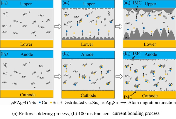
Fig. 10 Schematic diagram of Ag-GNSs reinforcing growth of IMC
In the present study, the electric current caused the dissolution of the Cu substrate. Additionally, Cu atoms were driven by the solid�Cliquid EM into the SAC matrix, leading to more Cu in the molten SAC solder. This increased the value of C0, thus forming a thick (0.98-4.27 ��m) layer of Cu6Sn5 at the Cu/solder interface in hundreds of milliseconds. As shown in the EDS of Cu at the cross-section in Fig. 6, the increase in the Cu6Sn5 volume fraction in the joints resulted in a higher Cu content in the grains and enabled more solute to build up at the interface. Moreover, the cooling rate was approximately 900 K/s owing to the good thermal conductivities of the joint and electrode material. Compared to the solidification in the reflow soldering, the constitutional supercooling that occurred at the front of the solid�Cliquid Cu-solder IMC interface was higher and could lead to the rapid formation of Cu6Sn5. Moreover, the plate-shaped Cu6Sn5 grains maintained the preferred  growth facets and [0001] growth direction [37]. The plate-shaped Cu6Sn5 grains were promoted by the higher Cu content build-up at the Cu6Sn5 interface via the solid�Cliquid EM, and the high cooling rate, which reduces the solute diffusion time and increases the interface roughening.
4.3 Shear strength effects due to Ag-GNSs and staggered plate-shaped Cu6Sn5
After the shear test, SEM with EDS was used to further observe the shear fracture surface to elucidate the damage behavior of the solder joints. The typical fracture morphologies of the reflow soldering joint and the cathode sides of the transient current bonding of the Cu/solder/Cu joints (100, 150, 200, and 250 ms) are shown in Figs. 11(a-e), respectively. For the reflow soldering joint (Fig. 11(a)), the joints can be observed to show a brittle fracture, which occurred in the IMC layer with a relatively smooth surface. However, as shown in Figs. 11(b-e), a mixture fracture pattern occurred in the transient current bonding joints. The morphology of the 100 ms joint visible in Fig. 11(b) is dimple-like with a small amount of brittle-like morphology at the junction of the IMC and SAC solder. The dimple side was composed of broken Cu6Sn5 while the brittle side comprised the SAC solder. As shown in Figs. 11(c-e), the fracture patterns for the 150 and 250 ms joints were still a mixture pattern of the ductile and brittle fracture. The fracture morphology and increased shear strength are composed of two significant parts: (1) brittle fracture that occurred in the plate-shaped IMCs; (2) dimples formed by the SAC solder. As shown in Fig. 11, this phenomenon is caused by the benefit from the uniform distribution of Ag-GNSs in the SAC matrix and the staggered plate-shaped Cu6Sn5 with a roughened surface by the transient current bonding.
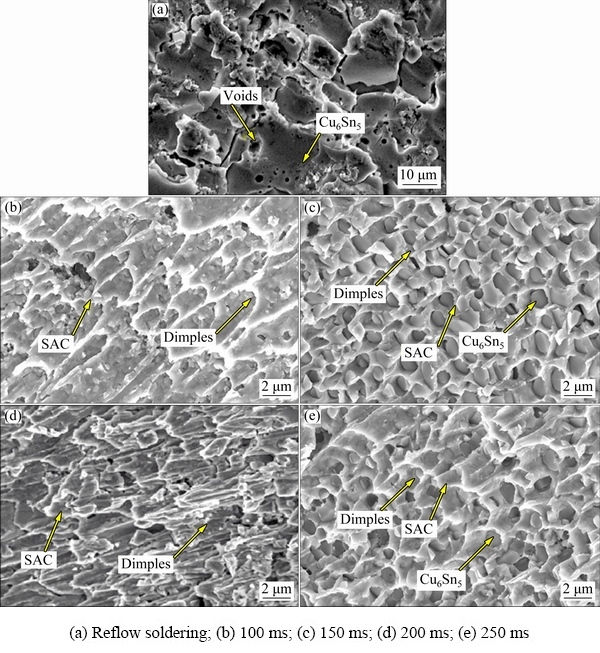
Fig. 11 SEM images of fracture surfaces
Research on the reinforced composite solder further confirms the existence and actual location of the reinforcing material in the joint. It has been introduced that shear fractures often occur between the IMCs and the SAC solder matrix [36]. Moreover, according to previous studies on the reinforcement added to the solder, reinforcements tended to aggregate on the IMC surface or phase interfaces. Similarly, the Ag-GNSs added to the SAC solder were obtained on the shear fracture surface, indicating an improvement in the joint mechanical properties arising from the Ag-GNSs in the joint. In this study, SEM images from a transient current bonding joint fracture surface (Figs. 12(a, c)) proved that several flakes were embedded in the solder matrix. As shown in the Raman spectra (Fig. 12(b)), three peaks (D, G, 2D) are the typical characteristic peaks of GNSs. Additionally, carbon was observed with an mole ratio of 39.94% in Fig. 12(d), confirming the Ag-GNS reinforcement in the matrices.
Furthermore, the dislocation density between the Ag-GNSs and the solder matrix can be increased via the thermal mismatch reported by HAN et al [40]. Because of the dispersion strengthening mechanism, the effects of adding GNSs with a larger surface area can increase the dislocation density and prevent the dislocation movement, which hinders the grain boundary sliding [4]. However, the improvement in the shear strength is ascribed to the load transfer behavior of the Ag-GNSs reinforcement in the SAC/Ag-GNSs solder matrix [41]. The load-transmitting behavior consists of two parts: interlocking effects and the van der Waals forces between the Ag-GNSs and the solder matrix. From Fig. 12(c), the GNSs appear to be incorporated into the solder matrix. Therefore, it can be observed that there is a reliable bond between the Ag-GNSs and the SAC solder.
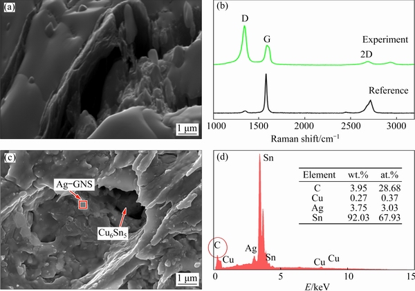
Fig. 12 SEM images of Ag-GNSs in SAC solder (a) and corresponding Raman spectra (b), and SEM image of Ag-GNSs on fracture surface (c) and corresponding EDS result (d)
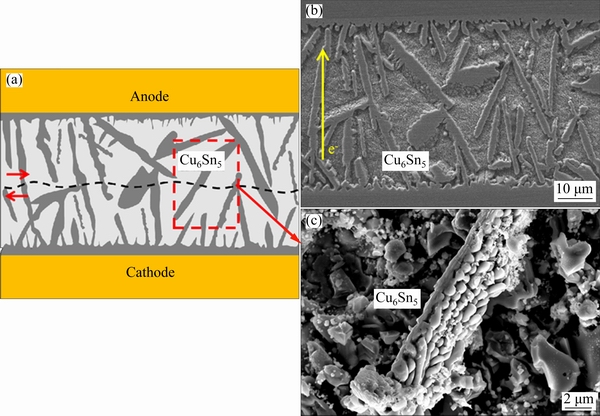
Fig. 13 Fracture diagram of plate-shaped Cu6Sn5 solder joints (a), and cross-section (b) and top-view (c) SEM images of plate-shaped Cu6Sn5 grains
In addition, the shear strength of the joint is determined by the Cu6Sn5 microstructure and the IMC interface. In the reflow soldering joint, as shown in Fig. 8(a), more voids occur in the thicker IMC layers. After 100 ms of solidification, the short rod-like Cu6Sn5 obtained at the interface and inside the material as well as a thinner IMC layer and fewer voids, enhanced the shear strength. Furthermore, as shown in Fig. 13(a), the plate- shaped Cu6Sn5 grains obtained by the electric current were staggered with small protrusions. After deep etching, the three-dimensional morphologies of the Cu6Sn5 (Figs. 13(b, c)) were obtained from the shear test joints. In the 200 and 250 ms joints, the plate-shaped Cu6Sn5 grains at the anode and cathode almost extended into the SAC solder and they were in contact. During the shear test process, a crack initially appeared in the middle of a plate-shaped Cu6Sn5 and then extended into the adjacent SAC solder. The Cu6Sn5 grains provide a higher surface area and interlocking structure, leading to higher shear strength of the joint. Thus, the plate-shaped Cu6Sn5 with small protrusions in the 250 ms bonding joints provided 45.0% higher shear strength compared to the 100 ms bonding joints.
5 Conclusions
(1) To melt the Cu/solder/Cu solder intermediate layer in the welding process, the Joule heating generated at the bonding interface was the primary heat source. At a current density of 1.0��104 A/cm2, the Cu/solder/Cu sandwich structure joints had higher shear strength than the reflow soldering joints.
(2) Compared to the reflow soldering joints, the Ag-GNSs were uniformly distributed in the transient current bonding joints and provided more nucleation sites in the solder to form homogeneous distribution of Cu6Sn5. Furthermore, the Cu-Sn interfaces of the cathode and anode produced similar plate-shaped IMC layers instead of the typical shell-like IMCs.
(3) With an increase in the transient current bonding time (100-250 ms), more Cu atoms can be promoted to dissolve into molten SAC/Ag- GNSs solder through solid�Cliquid EM and the Joule heating force. The microstructure of the Cu6Sn5 gradually changed from short rod-like to plate- shaped type, with more protrusions, which were attributed to constitutional supercooling.
(4) The improvement in shear strength owing to the addition of Ag-GNSs can be directly attributed to the uniform dispersion of the Ag-GNSs in the solder matrix and the staggered plate-shaped Cu6Sn5 with small protrusions. The shear strength of the 250 ms-bonded joints was 57.7 MPa, which was 159% higher than that of the reflow soldering joints.
Acknowledgments
The authors are grateful for the financial support from the National Natural Science Foundation of China (No. 51974198).
References
[1] QIN Yi, WILCOX G D, LIU Chang-qing. Electrodeposition and characterisation of Sn-Ag-Cu solder alloys for flip-chip interconnection [J]. Electrochimica Acta, 2011, 56(1): 183-192.
[2] CHIU T C, LIN K L. The difference in the types of intermetallic compound formed between the cathode and anode of an Sn-Ag-Cu solder joint under current stressing [J]. Intermetallics, 2009, 17(12): 1105-1114.
[3] BAATED A, KIM K S, SUGANUMA K, HUANG S, JURCIK B, NOZAWA S, UESHIMA M. Effects of reflow atmosphere and flux on Sn whisker growth of Sn-Ag-Cu solders [J]. Journal of Materials Science, 2010, 21: 1066-1075.
[4] HAN Yong-dian, GAO Yu, JING Hong-yang, WEI Jun, ZHAO Lei, XU Lian-yong. A modified constitutive model of Ag nanoparticle-modified graphene/Sn-Ag-Cu/Cu solder joints [J]. Materials Science and Engineering A, 2020, 777: 139080.
[5] WU C M L, YU Da-qun, LAW C M T, WANG L. Properties of lead-free solder alloys with rare earth element additions [J]. Materials Science and Engineering R, 2004, 44(1): 1-44.
[6] HUANG Ming-liang, ZHAO Ning, LIU Shuang, HE Yi-qian. Drop failure modes of Sn-3.0Ag-0.5Cu solder joints in wafer level chip scale package [J]. Transactions of Nonferrous Metals Society of China, 2016, 26(6): 1663-1669.
[7] SHAO Hua-kai, WU Ai-ping, BAO Yu-dian, ZHAO Yue, ZOU Gui-sheng. Mechanism of Ag3Sn grain growth in Ag/Sn transient liquid phase soldering [J]. Transactions of Nonferrous Metals Society of China, 2017, 27(3): 722-732.
[8] BABAGHORBANI P, NAI S M L, GUPTA M. Reinforcements at nanometer length scale and the electrical resistivity of lead-free solders [J]. Journal of Alloys and Compounds, 2009, 478(1-2): 458-461.
[9] TSAO L C, HUANG Chi-hui, CHUANG Chien-han, CHEN R S. Influence of TiO2 nanoparticles addition on the microstructural and mechanical properties of Sn0.7Cu nano-composite solder [J]. Materials Science and Engineering A, 2012, 545: 194-200.
[10] YANG Zhong-bao, ZHOU Wei, WU Ping. W. Effects of Ni-coated carbon nanotubes addition on the electromigration of Sn-Ag-Cu solder joints [J]. Journal of Alloys and Compounds, 2013, 581: 202-205.
[11] ZHANG Xiang-zhao, WU Xiao-lang, LIU Gui-wu, LUO Wen-qiang, GUO Ya-jie, SHAO Hai-cheng, QIAO Guan-ju. Wetting of molten Sn-3.5Ag-0.5Cu on Ni-P(-SiC) coatings deposited on high volume faction SiC/Al composite [J]. Transactions of Nonferrous Metals Society of China, 2018, 28(9): 1784-1792.
[12] MALLIKARJUNA H M, KASHYAP K T, KOPPAD P G, RAMESH C S, KESHAVAMURTHY R. Microstructure and dry sliding wear behavior of Cu-Sn alloy reinforced with multiwalled carbon nanotubes [J]. Transactions of Nonferrous Metals Society of China, 2016, 26(7): 1755-1764.
[13] SHARMA A, SOHN H, JUNG J P. Effect of graphene nanoplatelets on wetting, microstructure, and tensile characteristics of Sn-3.0Ag-0.5Cu (SAC) alloy [J]. Metallurgical and Materials Transactions A, 2016, 47: 494-503
[14] YANG Wen-hua, ZHOU Jie, JIANG Xin-yuan, YE Xi-ming, XUAN Xiao-feng, WU Chun-yan, LUO Lin-bao. Cu-Cu low temperature bonding based on lead-free solder with graphene interlayer [J]. Applied Physics Letters, 2019, 115(12): 122102.
[15] MOKHTARI O, ROSHANGHIAS A, ASHAYER R, KOTADIA H R, KHOMAMIZADEH F, KOKABI A H, CLODE M P, MIODOWNIK M, MANNAN S H. Disabling of nanoparticle effects at increased temperature in nanocomposite solders [J]. Journal of Electronic Materials, 2012, 41(7): 1907-1914.
[16] WANG Hui-gai, ZHANG Ke-ke, ZHANG Meng. Fabrication and properties of Ni-modified graphene nanosheets reinforced Sn-Ag-Cu composite solder [J]. Journal of Alloys & Compounds, 2019, 781: 761-772.
[17] KHODABAKHSHI F, SAYYADI R, JAVID N S. Lead free Sn-Ag-Cu solders reinforced by Ni-coated graphene nanosheets prepared by mechanical alloying: Microstructural evolution and mechanical durability [J]. Materials Science and Engineering A, 2017, 702: 371-385.
[18] CHEN Guang, WU Feng-shun, LIU Chang-qing, SILBERSCHMIDT V V, CHAN Y C, Microstructures and properties of new Sn-Ag-Cu lead-free solder reinforced with Ni-coated graphene nanosheets [J]. Journal of Alloys and Compounds, 2016, 656: 500-509.
[19] XU Lian-yong, CHEN Xi, JING Hong-yang, WANG Li-xia, WEI Jun, HAN Yong-dian. Design and performance of Ag nanoparticle-modified graphene/SnAgCu lead-free solders [J]. Materials Science and Engineering A, 2016, 667: 87-96.
[20] ZHANG Rui, TIAN Yan-hong, HANG Chun-jin, LIU Bao-lei, WANG Chun-qing. Formation mechanism and orientation of Cu3Sn grains in Cu-Sn intermetallic compound joints [J]. Materials Letters, 2013, 110: 137-140.
[21] ZHAO Guo-ji, WEN Guang-hua, SHENG Guang-min. Influence of rapid solidification on Sn-8Zn-3Bi alloy characteristics and microstructural evolution of solder/Cu joints during elevated temperature aging [J]. Transactions of Nonferrous Metals Society of China, 2017, 27(1): 234-240.
[22] JI Hong-jun, QIAO Yun-fei, LI Ming-yu. Rapid formation of intermetallic joints through ultrasonic-assisted die bonding with Sn-0.7Cu solder for high temperature packaging application [J]. Scripta Materialia, 2016, 110: 19-23.
[23] LI Zhuo-lin, LI Ming-yu, XIAO Yong, WANG Chun-qing. Ultrarapid formation of homogeneous Cu6Sn5 and Cu3Sn intermetallic compound joints at room temperature using ultrasonic waves [J]. Ultrasonics Sonochemistry, 2014, 21(3): 924-929.
[24] FU Zi-wei, ZHOU Bin, YAO Ruo-he, LIU Y R, LI X P. Electromigration effect on kinetics of Cu-Sn intermetallic compound growth in lead-free solder joint [J]. IEEE Transactions on Device and Materials Reliability, 2017, 17(4): 773-779.
[25] LIU C Y, HU Y J, LIU Y S, TSENG H W, HUANG Tsai-shang, LU C T, CHUANG Y C, CHENG S L. Epitaxial Cu-Sn bulk crystals grown by electric current [J]. Acta Materialia, 2013, 61(15): 5713-5719.
[26] ATTARI V, GHOSH S, DUONG T, ARROYAVE R. On the interfacial phase growth and vacancy evolution during accelerated electromigration in Cu/Sn/Cu microjoints [J]. Acta Materialia, 2018, 160: 185-198.
[27] TANG Wen-ming, HE An-qiang, LIU Qi, IVEY D G. Solid state interfacial reactions in electrodeposited Cu/Sn couples [J]. Transactions of Nonferrous Metals Society of China, 2010, 20(1): 90-96.
[28] MEI Yun-hui, CAO Yun-jiao, CHEN Gang, LI Xin, LU Guo-quan, CHEN Xu. Rapid sintering nanosilver joint by pulse current for power electronics packaging [J]. IEEE Transactions on Device and Materials Reliability, 2013, 13(1): 258-265.
[29] LIU Bao-lei, TIAN Yan-hong, WANG Chen-xi, AN Rong, LIU Yang. Extremely fast formation of Cu Sn intermetallic compounds in Cu/Sn/Cu system via a micro-resistance spot welding process [J]. Journal of Alloys and Compounds, 2016, 687: 667-673.
[30] FENG Jia-yun, HANG Chun-jin, TIAN Yan-hong, LIU Bao-lei, WANG Chen-xi. Growth kinetics of Cu6Sn5 intermetallic compound in Cu-liquid Sn interfacial reaction enhanced by electric current [J]. Scientific Reports, 2018, 8(1): 1775.
[31] LIU Bao-lei, TIAN Yan-hong, FENG Jia-yun, WANG Chen-xi. Enhanced shear strength of Cu-Sn intermetallic interconnects with interlocking dendrites under fluxless electric current-assisted bonding process [J]. Journal of Materials Science, 2017, 52(4): 1943-1954.
[32] AHMRD M, FOUZDER T, SHARIF A, GAIN A K, CHAN Y C. Influence of Ag micro-particle additions on the microstructure, hardness and tensile properties of Sn-9Zn binary eutectic solder alloy [J]. Microelectronics Reliability, 2010, 50(8): 1134-1141.
[33] CHOUNDHURY S F, LADANI L. Miniaturization of micro-solder bumps and effect of IMC on stress distribution [J]. Journal of Electronic Materials, 2016, 45(7): 3683-3694.
[34] ZHAO Xin, ZHANG Qing-hua, CHEN Da-jun, LU Ping. Enhanced mechanical properties of graphene-based poly(vinyl alcohol) composites [J]. Macromolecules, 2010, 43(5): 2357-2363.
[35] MA Hong-tao, SUJLING J C. A review of mechanical properties of lead-free solders for electronic packaging [J]. Journal of Materials Science, 2009, 44(5): 1141-1158.
[36] KIM H K, TU K N. Kinetic analysis of the soldering reaction between eutectic SnPb alloy and Cu accompanied by ripening [J]. Physical Review B, 1996, 53(23): 16027-16034.
[37] XIAN J W, BELYAKOV S A, OLLIVER M, NOGITA K, YASUDA H, GOURLAY C M. Cu6Sn5 crystal growth mechanisms during solidification of electronic interconnections [J]. Acta Materialia, 2017, 126: 540-551.
[38] JACKSON K A. Constitutional supercooling surface roughening [J]. Journal of Crystal Growth, 2004, 264(4): 519-529.
[39] VADUKUMPULLY S, PUAL J, MAHANTA N, VALIYAVEETTI S. Flexible conductive graphene/poly (vinyl chloride) composite thin films with high mechanical strength and thermal stability [J]. Carbon, 2011, 49(1): 198-205.
[40] HAN Yong-dian, GAO Yu, ZHANG Shu-ting, JING Hong-yang, WEI Jun, ZHAO Lei, XU Lian-yong. Study of mechanical properties of Ag nanoparticle-modified graphene/Sn-Ag-Cu solders by nanoindentation [J]. Materials Science and Engineering A, 2019, 761: 138051.
[41] YANG Ming, LI Ming-yu, WANG Ling, FU Yong-gao, KIM J, WENG Lv-qian. Cu6Sn5 morphology transition and its effect on mechanical properties of eutectic Sn-Ag solder joints [J]. Journal of Electronic Materials, 2011, 40(2): 176-188.
������1,2�������1,2�������� 1,2�������� 1,2���� �� 1,2
1. ����ѧ ���Ͽ�ѧ�빤��ѧԺ����� 300350��
2. ������ִ����Ӽ����ص�ʵ���ң���� 300350
ժ Ҫ��Ϊ���о�Ag����ʯīϩ��ǿ��Sn-Ag-Cu(SAC/Ag-GNSs)�����ڴ�ͳ������������Ag-GNSs���۳����ϸ��ۼ����⣬���õ����ܶ�(1.0��104 A/cm2)�ڼ��ٺ�����ʵ��Cu-SAC/Ag-GNSs-Cu��ͷ���ټ��ϡ����������Ag-GNSs���ȷ�ɢ�ں����У�ΪCu6Sn5�����ɺ��ṩ�����κ�λ�㣬�Ӷ�ϸ���������������������������Ȳ���⣬����Ag-GNSs�ľ��ȷֲ�����֯���䣬Cu6Sn5����ò�ɰ�״ת��Ϊ��״��ͬʱ��˲̬�������Ϲ��պ������ǿ�ȵ�������ߺͶ��ѻ����ı仯�����ھ��ȷֲ���Ag-GNSs�����ṹ�仯��
�ؼ��ʣ�����˲̬���ϣ�Ag����ʯīϩ��Cu6Sn5������ǿ��
(Edited by Xiang-qun LI)
Corresponding author: Lian-yong XU, Tel: +86-13920370051, E-mail: xulianyong@tju.edu.cn
DOI: 10.1016/S1003-6326(21)65666-2
1003-6326/ 2021 The Nonferrous Metals Society of China. Published by Elsevier Ltd & Science Press

