
Localized CO2 laser bonding process for MEMS packaging
SUN Li1, A. P. MALSHE1, S. CUNNINGHAM2, A. MORRIS3
1. Department of Mechanical Engineering, University of Arkansas, Fayetteville, AR 72701, USA;
2. wiSpry Inc., Irvine, CA 92618, USA; 3. wiSpry Inc., Cary, NC 27513, USA
Received 10 April 2006; accepted 25 April 2006
Abstract: The packaging poses a critical challenge for commercialization of MEMS products. Major problems with the packaging process include degraded reliability caused by the excess stress due to thermal mismatch and altered performance of the MEMS device after packaging caused by thermal exposure. The localized laser bonding technique for ceramic MEMS packaging to address above-mentioned challenges was investigated. A continuous wave CO2 laser was used to locally heat sealing material for ceramic MEMS package lid to substrate bonding. To determine the laser power density and scanning speed, finite element analysis thermal models were constructed to simulate the localized laser bonding process. Further, the effect of external pressure at sealing ring on the bonding formation was studied. Pull testing results show that the scanning speed and external pressure have significant influence on the pull strength at the bonding interface. Cross-sectional microscopy of the bonding interface indicates that the packages bonded with relatively low scanning speed and external pressure conditions have higher bonding quality. This research demonstrates the potential of localized laser bonding process for ceramic MEMS packaging.
Key words: localized laser bonding; MEMS packaging; FEA; mechanical pull tests; cross-sectional microscopy
1 Introduction
Micro-Electro-Mechanical Systems (MEMS) are meso-to-submicron scale mechanical moving parts and assemblies developed for sensing and actuation purposes. Their diverse applications are in areas such as radio frequency (RF) switches and antennas, biomedical fluidic drug delivery system and implants, optical displays and switches, chemical reactors and fuel cells, etc [1]. According to its application requirements, every MEMS device needs an application specific interface, typically called a package, to interact with application environment. The package provides aspects as follows.
1) Physical support for mounting.
2) Interconnections from chip-to-physical support and a window to the outside environment and data processing interface.
3) At the same time, protection from the outside world.
4) Waste management (heat, fluid, stray light).
These attributes clearly distinguish MEMS packaging from the traditional IC packaging .
Due to the requirement of application specific packaging, most MEMS packaging accounts for 50%-70% cost of final products, which remains an expensive roadblock for rapid commercialization of MEMS [2]. Another factor is the effect the package and packaging process can have on the MEMS device. It is important to address the package and the MEMS devices as a coupled design problem to address the thermal mismatch between package and MEMS, which can often result in reduced reliability [3, 4]. Another important consideration is the hermeticity capability of the package relative to an exchange of gas or moisture. A final consideration is a change in the MEMS performance caused by the thermal history of the packaging process [5].
To address the above-mentioned issues, local heating and rapid heating approaches, such as resistive micro-heaters [6], rapid thermal processing (RTP) [7], and laser bonding [8-10], have been developed for MEMS packaging. Particularly, laser processing is of interest due to [11] the following aspects.
1) Tight control on the time and temperature win-dow for processing.
2) Non-contact processing.
3) Processing of complex shapes.
4) Opportunity to select various suitable wavel-engths, depending upon the wafer materials
5) Region selectivity.
6) Fast manufacturing.
In this research work, the localized laser bonding process for ceramic MEMS packaging was investigated. This process has been demonstrated for CQFP packaging in our previous research [12]. In this paper, the material system was extended, and finite element analysis (FEA) thermal models were constructed to understand the effect of laser processing parameters on the temperature distribution. Further, more processing parameters including laser power density, scanning speed, and external pressure were studied and discussed for the localized laser bonding process of ceramic MEMS packages.
2 FEA thermal modeling
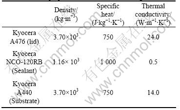
It is key to control temperature to form bonding and to minimize the effect of packaging process (heating) on the MEMS device and change in the MEMS performance caused by the thermal history of the packaging process. In this research, the temperature distribution during bonding was mainly controlled by the laser power density and the scanning speed. A FEA thermal model was constructed with ANSYS 9.0 to understand the effect of laser power density and the scanning speed on the packaging temperature. Fig.1 illustrates the thermal model for heat transfer analysis of 4 mm×4 mm ceramic packages. Packaging material properties used in the modeling are listed in Table 1.
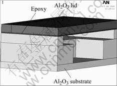
Fig. 1 FEA thermal model for heat transfer analysis
In the thermal analysis, the whole model was set to 22 ℃ as an initial condition. The boundary conditions were defined as follows.
1) Outer surfaces exposed to air were treated to be insulated (Based on the theoretical calculation, energy loss through convection and radiation was less than 3% of the energy input by the laser. Therefore, convection and radiation were ignored in the model).
Table 1 Material properties used for FEA modeling
2) Laser power density was applied as a heat flux of 18 MW/m2.
3) Scanning speed was set to be 0.5 mm/s (This was used to simulate the moving of the sample stage. It was realized by applying the heat flux on a sequence of elements according to the process time).
4) The temperature of bottom surface of the package was fixed at 30 ℃.
A representative modeling result is shown in Fig.2. It can be seen that the temperature at the sealing layer is around 180 ℃, a little higher than the glass transition point 150 ℃. The highest temperature on the lid is around 360 ℃. The high temperature region is confined in a small area, which is favorable for minimal thermal effect on the MEME device inside the package.

Fig.2 Temperature distribution on package during localized laser bonding process
To understand the thermal history of the package, a specific node (node 1) was taken to record the temperature changed with time, as shown in Fig.3. It can be seen that temperature changes fastly with time, on the order of a few seconds. This is desirable to reduce the influence of packaging process on the MEMS device.
The modeling results provide a guideline for selection of the laser bonding parameters and assist optimization of the packaging process. The selection of the parameters depends on considerations of temperature distribution at the sealing layer, time requirement for the materials to form bonding, thermo-mechanical stress
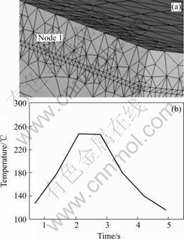
Fig.3 Temperature history at node 1
after bonding, and temperature distribution/history at the devices. More parameter studies for laser bonding of MEMS packages are in progress.
3 Experimental
The ceramic packages used in this research work were from wiSpry Inc. with material properties specified in Table 1. The lids were 4.00 mm×4.00 mm×0.25 mm in dimension with a 30 μm thick epoxy layer. The substrates were 4.00 mm×4.00 mm×1.10 mm in dimension.
A continuous wave CO2 laser was used for the laser bonding process. The laser (model 3 080) was from Preco Inc. with a wavelength of 10.6 ?m. The theoretical focused spot size of the laser beam is calculated to be 0.34 mm in diameter. A piece of plexiglass was exposed to the laser beam at the focal distance for a short exposure duration to confirm the calculation. The diameter of the burned region on the plexiglass was approximated to be the focused laser beam spot size. Using this method, the laser beam focused spot size is measured to be around 0.5 mm in diameter at the focal distance.
Fig.4 shows the schematic diagram of the experimental setup. The output from the laser was delivered to the sample using an optical beam delivery system. The beam was focused on the package using a 25.4 mm diameter planoconvex lens with an effective focal length of 254 mm. A power meter (Ophir Inc., model Laser Star) were used to check the incident power of the laser beam. The sample stage was mounted on a computer controlled speed rate screw driven X-Y translation stage (Velmex Inc., make MN10 bislide assembly).
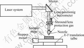
Fig. 4 Schematic diagram of experimental setup
4 Results and discussion
4.1 Mechanical pull testing
Pull tests using a material strength testing instrument (The Quad Group Inc., SEBASTIAN FIVE-A) were performed to measure the bonding strength. According to the FEA modeling results, a few trials of laser bonding were conducted to determine the range of laser bonding parameters. Then specific parameters were applied for bonding the ceramic packages. The results of pull tests are summarized in Table 2.
Table 2 Pull strength of laser bonded packages with varied processing parameters
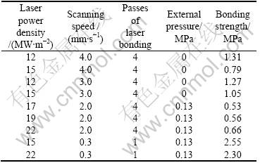
It can be seen that the pull strength of laser bonded packages form three distinct groups. When no external pressure is applied on the sealing ring, the bonding strength is around 1 MPa. When external pressure is applied (by putting potassium bromide, which is nearly 100% transparent to the 10.6 ?m wavelength infrared light, on the package lid) and scanning speed is 2 mm/s, the bonding strength is around 0.6 MPa. In the last group, the bonding strength is around 2.5 MPa when external pressure is applied and scanning speed is 0.3 mm/s. This observation shows that the external pressure and scanning speed have significant effects on the bonding strength of the packages. Comparing the bonding strength, it is evident that applied external pressure and low scanning speed are preferable in the current setup to obtain higher lid to substrate bonding strength of the ceramic packages.
4.2 Cross-sectional microscopy
To understand the reason for varied pull strength of laser bonded packages with different processing conditions, the packages were cross-sectioned and polished with a polisher (Buehler, Inc., model 60-1950-160) to reveal the bonding interface. The cross-section was then observed under a microscope (Nikon Inc., model EPIPHOT? 200). Fig.5 shows a representative cross-sectional picture of packages bonded without external pressure applied on the sealing ring.
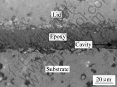
Fig.5 Bonding interface of packages processed at 12 MW/m2, 3 mm/s, 4 passes, and no external pressure applied on sealing ring
It can be seen that the bonding between epoxy and substrate is partially formed after laser processing. However, unbonded areas still presente forming cavities at the bonding interface. These unbonded areas are strength limiting points and thus need to be removed. To improve the bonding quality, external pressure was applied. Fig.6 illustrates a cross-sectional view of a package processed with an external pressure of 0.13 MPa and scanning speed of 2 mm/s.
Compared to the case in Fig.5, the gap between epoxy and substrate is much larger after the external pressure is applied, which is consistent with the lower pull strength (around 0.6 MPa) in this case. It is believed that the reason for formation of the big gap is the acceleration and deceleration of the sample stage. When potassium bromide is placed on the lid, relative movement between lid and substrate or uneven load may form when the package is moving with a relatively high acceleration, which resultes in the undesirable big gap at bonding interface. To investigate the effect of scanning
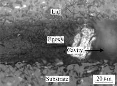
Fig.6 Bonding interface of packages processed at 22 MW/m2, 2 mm/s, 4 passes, and 0.13 MPa external pressure applied on sealing ring
speed/acceleration further, low scanning speed was applied. Fig.7 shows a representative cross-sectional picture of packages processed with an external pressure of 0.13 MPa and scanning speed of 0.3 mm/s.
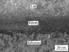
Fig.7 Bonding interface of packages processed at 15 MW/m2, 0.3 mm/s, 1 passes, and 0.13 MPa external pressure applied on sealing ring
It is evident that bonding is formed between epoxy and substrate, which results in a higher bonding strength (around 2.5 MPa) in this case. This observation also confirms that the low scanning speed is favorable to improve the bonding quality.
5 Conclusions
The localized laser bonding process for ceramic MEMS packaging was established. A FEA thermal model was constructed to simulate the laser bonding process and provide guideline for experimental work. Ceramic packages were sealed using a CO2 laser with a set of combinations of processing parameters including various laser power densities, scanning speeds and external pressures. The effect of the processing parameters was examined with pull tests and cross-sectional microscopy. It is concluded that scanning speed and external pressure have significant influence on the bonding strength at the bonding interface. Low scanning speed and applied external pressure are preferable for high quality bonding.
Acknowledgments
This work is sponsored by WiSpry Inc. and ECS-NSF (0501597). The experiments were conducted in Material and Manufacture Research Laboratories (MRL), University of Arkansas.
References
[1] DRESSENDORFER P V, PETERSON D A, REBER C A. MEMS packaging-current issues and approaches[A]. Proceedings 2000 HD International Conference on High-Density Interconnect and Systems Packaging [C]. Reston: IMAPS, 2000, 4217: 208-213.
[2] MALSHE A. P, O’NEAL C, SINGH S B, BROWN W D, EATON W P, MILLER W M. Challenges in the packaging of MEMS[J]. International Journal of Microcircuits and Electronic Packaging, 1999, 22(3): 233-241.
[3] MERCADO L L, LEE T T, KUO S M, LEE R. Process-induced thermal effect on packaging yield of RF MEMS switches[A]. American Society of Mechanical Engineers, EEP, v 2, Electronic and Photonic Packaging, Electrical Systems and Photonics Design and Nanotechnology[C]. New Orleans: ASME, 2002, 25-32.
[4] DE SILVA A. P, LIU L, HUGHES H G. Impact of Thermal Cycles During the Packaging Assembly Process on RF-MEMS Switch Performance[A]. Proceedings of SPIE-The International Society for Optical Engineering International Symposium on Microelectronics[C]. Boshton: The International Society for Optical Engineering, 2003, 5288: 407-411.
[5] REBEIZ G M, RF MEMS Theory, Design, and Technology[M]. Hoboken: John Wiley & Sons Inc, 2003.
[6] LIN L. MEMS post-packaging by localized heating and bonding[J]. IEEE Transactions on Advanced Packaging, 2000, 23(4): 608-616.
[7] CHIAO M, LIN L. Hermetic wafer bonding based on rapid thermal processing[J]. Sensors and Actuators, A: Physical, 2001, 90(3): 398-402.
[8] WILD M J, GILLNER A, POPRAWE R. Locally selective bonding of silicon and glass with laser[J] Sensors and Actuators A: Physical, 2001, 93: 63-69.
[9] LUO C, LIN L. The application of nanosecond-pulsed laser welding technology in MEMS packaging with a shadow mask[J]. Sensors and Actuators A: Physical, 2002, 97-98: 398-404.
[10] MESCHEDER U M, ALAVI M, HILTMANN K, LIETZAU Ch, NACHTIGALL Ch, SANDMAIER H. Local laser bonding for low temperature budget[J]. Sensors and Actuators A: Physical, 2002, 97-98: 422-427.
[11] TAO Y, MALSHE A P, BROWN W D. Selective bonding and encapsulation for wafer-level vacuum packaging of MEMS and related micro systems[J]. Microelectronics Reliability, 2004, 44(2): 251-258.
[12] TAO Y, MALSHE A P, BROWN W D, DEREUS D R, CUNNINGHAM S. Laser-assisted sealing and testing for ceramic packaging of MEMS devices[J]. IEEE Transactions on Advanced Packaging, 2003, 26(3): 283-288.
(Edited by ZHAO Jun)
Corresponding author: A. P. MALSHE; Tel: +1-479-575-6561; Fax: +1-479-575-6982; E-mail: apm2@engr.urak.edu

