Ultra-low temperature anodic bonding of silicon and glass based on nano-gap dielectric barrier discharge
来源期刊:中南大学学报(英文版)2021年第2期
论文作者:潘明强 姚富荣 朱宗建 刘吉柱 WANG Yang-jun(王阳俊)
文章页码:351 - 360
Key words:dielectric barrier discharge; anodic bonding; ultra-low temperature
Abstract: The article improves the process of dielectric barrier discharge (DBD) activated anode bonding. The treated surface was characterized by the hydrophilic surface test. The results showed that the hydrophilic angle was significantly reduced under nano-gap conditions and the optimal discharge voltage was 2 kV. Then, the anodic bonding and dielectric barrier discharge activated bonding were performed in comparison experiments, and the bonding strength was characterized by tensile failure test. The results showed that the bonding strength was higher under the nano-gap dielectric barrier discharge. This process completed 110 °C ultra-low temperature anodic bonding and the bonding strength reached 2 MPa. Finally, the mechanism of promoting bonding after activation is also discussed.
Cite this article as: YAO Fu-rong, PAN Ming-qiang, ZHU Zong-jian, LIU Ji-zhu, WANG Yang-jun. Ultra-low temperature anodic bonding of silicon and glass based on nano-gap dielectric barrier discharge [J]. Journal of Central South University, 2021, 28(2): 351-360. DOI: https://doi.org/10.1007/s11771-021-4607-z.

J. Cent. South Univ. (2021) 28: 351-360
DOI: https://doi.org/10.1007/s11771-021-4607-z

YAO Fu-rong(姚富荣)1, 2, 3, PAN Ming-qiang(潘明强)1, 2, 3, ZHU Zong-jian(朱宗建)1, 2, 3,LIU Ji-zhu(刘吉柱)1, 2, 3, WANG Yang-jun(王阳俊)1, 2, 3
1. College of Mechatronics Engineering & Collaborative Innovation Center of Suzhou Nano Science and Technology, Soochow University, Suzhou 215123, China;
2. Jiangsu Key Laboratory for Advanced Robotics Technology, Soochow University, Suzhou 215123, China;
3. Robotics and Microsystems Center, Soochow University, Suzhou 215123, China
 Central South University Press and Springer-Verlag GmbH Germany, part of Springer Nature 2021
Abstract: The article improves the process of dielectric barrier discharge (DBD) activated anode bonding. The treated surface was characterized by the hydrophilic surface test. The results showed that the hydrophilic angle was significantly reduced under nano-gap conditions and the optimal discharge voltage was 2 kV. Then, the anodic bonding and dielectric barrier discharge activated bonding were performed in comparison experiments, and the bonding strength was characterized by tensile failure test. The results showed that the bonding strength was higher under the nano-gap dielectric barrier discharge. This process completed 110 °C ultra-low temperature anodic bonding and the bonding strength reached 2 MPa. Finally, the mechanism of promoting bonding after activation is also discussed.
Key words: dielectric barrier discharge; anodic bonding; ultra-low temperature
Cite this article as: YAO Fu-rong, PAN Ming-qiang, ZHU Zong-jian, LIU Ji-zhu, WANG Yang-jun. Ultra-low temperature anodic bonding of silicon and glass based on nano-gap dielectric barrier discharge [J]. Journal of Central South University, 2021, 28(2): 351-360. DOI: https://doi.org/10.1007/s11771-021-4607-z.
1 Introduction
WALLIS and POMERANTZ [1] developed anodic bonding in 1969, also known as field assisted bonding. The advantage of anodic bonding is that the bonding temperature is lower than the melting point of the bonded sample [2] and contributes to achieving high bonding strength [3]. As a result, it has become a key bonding technology for fabricating microelectromechanical systems (MEMS) packages. It plays an important role in packaging RF MEMS devices, 3D stacking in advanced packaging, and improving MEMS power performance or vacuum packaging. Since the connection using anodic bonding is characterized by high adhesive strength, high chemical resistance and air tightness, it is used in the integration of micro light-emitting diodes (LEDs) or optical detectors, and anodic bonding is used to form a sealed optical cap [4], construction of vacuum sealed vapor chambers for optical spectroscopy [5], microlens arrays [6], 3D microlens scanners [7, 8], based on microfluidic optical detection systems [9], micro-optical magnetic forces [10], and micro-optical choppers for Raman spectroscopy [11]. In addition, it is used in vacuum for integrated pressure sensors [12], accelerometers [13] and gyroscopes [14] and for assembly at atmospheric pressure micro fluidic systems [15], electron beam lenses [16] and atomic force microscope probes [17]. The basic principle of the traditional anodic bonding is to use high temperature (400-500 °C) to improve the internal energy of the bonding interface chemical bond, and soften the microscopic layer of the glass interface, and then the contact point under the electric field to form a bonding point, and under pressure synergistically, micro-creep is generated at the glass interface to expand the bonding points to form a bonding layer [18]. Therefore, high temperature is one of the key conditions for the realization of conventional anodic bonding. Due to the uneven distribution of thermal field, differential thermal response of materials, and high temperature reaction, the traditional bonding process is prone to thermal stress and thermal deformation, which may affect or even impair the performance of MEMS devices. For example, atomic interferometer magnetometers, atomic clocks, atomic gyros and other quantum instruments, the core alkali metal atomic chamber, and the alkali metal are chemically active, and the temperature is too high to produce a chemical reaction. The high package temperature of these devices will directly lead to the failure of device fabrication [19]. The structures widely used in MEMS devices, such as the micro-beam, thin-wall and thin film, are affected by the thermal stress and thermal deformation of traditional bonding, which always restricts the overall performance of the device. In addition, the gas in the glass micro pores expands and overflows because of the high temperature. It is easy to form a local gas layer at the bonding interface, causing hole defects and affecting product yield. In order to obtain high-performance electrical and optical interfaces, bonding at low temperatures is required. Low-temperature bonding minimizes misalignment caused by CTE differences and stress between materials, thereby improving optical coupling efficiency and interconnection reliability [20]. Therefore, such packages require as much anodic bonding temperature as possible. With the rapid development of MEMS technology, the problem of traditional high-temperature bonding heat is becoming more and more serious, which has become a bottleneck restricting the development of MEMS technology.
In order to lower the bonding temperature and increase the bonding strength, the Si and glass surfaces are treated with plasma, and then anodic bonding is carried out [21]. In plasma processing techniques, it has been well established that plasma generated by exposure to inert gases and/or reactive gases can clean the surface of the material and change its properties, especially its surface energy. The active material from the plasma bombardment reacts with a monolayer on the surface of the material and temporarily or permanently changes its surface properties [22]. Since plasma technique can effectively achieve the modification of the near-surface region without affecting the overall properties of the material [23]. Common discharge methods include dielectric barrier discharge, and corona discharge. DBD has its own advantages. For example, DBD produces more uniform and more active particles than corona discharge, and it has better process compatibility with anode bonding.
2 Experimental
2.1 Experiment device
In this test, a glass substrate (Borofloat 3.3, Shott) having dimensions of 10 mm×10 mm and a thickness of 0.5 mm was used. The silicon wafers used in the test was 5 mm×5 mm with a thickness of 0.4 mm. The glass substrate was placed on a heating platform (also a test power supply electrode), and the silicon wafer was stacked on the glass substrate and connected to the other end of the power electrode through the needle electrode.
A schematic of a dielectric barrier discharge anodic bonded composite device is shown in Figure 1(c). The CTP 2000 K (Coronalab, China) plasma power supply was used to provide high applied voltage. The operating frequency of the power supply can be adjusted from 10 to 40 kHz. The discharge load consisted of an upper electrode, a blocking medium, an air gap and a lower electrode. The anodic bonding voltage was adjustable by high voltage DC power supply, and the adjustable range was 0-3000 V.
2.2 Sample pretreatment
At present, the plasma activated bonding technology mostly uses a step-by-step pretreatment process. The two steps of pretreatment and bonding are not on the same station. After the pretreatment step is completed, the bonding step can be performed after the transfer. In this way, the surface pretreatment is performed. The controllability of the performance becomes worse. This study combines the currently commonly used pretreatment process of the dielectric barrier plasma discharge interface activation pretreatment with the anode bonding process. Since the dielectric barrier discharge structure of the flat electrode is similar to the structure of the anode bonding device, they can be integrated on the same station to achieve low temperature and efficient anodization. The flat-type dielectric barrier discharge is shown in Figure 1(a), using an air suction device to adsorb silicon, forming an air gap with glass and generating plasma in the air gap for activation, as shown in Figure 1(b). Then, silicon is moved to the glass surface, and perform anodic bonding. As shown in Figure 1(c), after the improvement, silicon is directly laminated on the glass surface, and the air gap formed by the surface roughness is used to discharge, as shown in Figure 1(d). After activation, anodic bonding is performed directly, which simplifies one process.
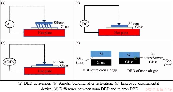
Figure 1 Experimental device:
For the conventional dielectric barrier discharge, the air gap is on the order of millimeters, which is called millimeter DBD. The dielectric gap discharge system has an air gap on the order of nanometers, which is called nano DBD. For micron DBD, a hydrophilic angle of 10° and below is an excellent hydrophilic surface. For nano DBD, a series of tests have been done to set the discharge frequency as 10 kHz and the time as 60 s each time. The test results are shown in Table1.
At 2000-2500 kV, the treatment effect is significantly better; further, set the discharge voltage to 1900-2600 V; increase 100 V each time; repeat the test three times with the same parameters. The results are shown in Figures 2 and 3. It can be found from Figures 2 and 3 that when the voltage is less than 2100 V, the surface treatment fails less and the effect is better.
Table 1 Hydrophilic angle when bonding voltage is 0-3000 kV
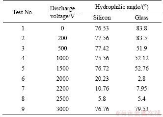
Some results reached about 10°. The effect of this part is similar to that of the milimeter DBD optimal treatment surface. However, some hydrophilic angles are abnormal. Since both silicon and the furnace are conductors, when the voltage is too high, the air between the silicon and the furnace is decomposed, and the discharge extends from the silicon around the glass to the furnace. Therefore, the processing area is the glass edge, as shown in Figure 4. A smaller discharge voltage needs to be selected, so 2000 V is selected as the discharge processing parameter.
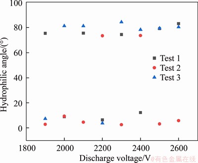
Figure 2 Hydrophilic angle of silicon when bonding voltage is 1900-2600 V
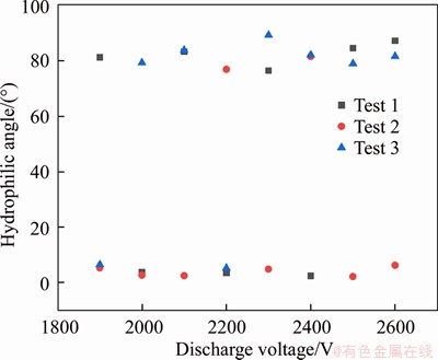
Figure 3 Hydrophilic angle of glass when bonding voltage is 1900-2600 V
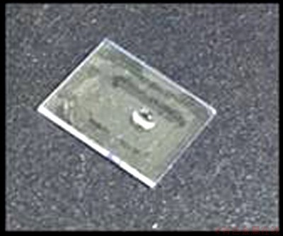
Figure 4 Surface after wrong activation
2.3 Bond current test
Anodic bonding is generally considered to be an electrochemical process. The bonding current was measured by an Agilent Technologies 34410A digital ammeter. In a combined system of silicon and glass, silicon was connected to the anode, glass was connected to the cathode, and the ammeter was connected in series to the negative electrode.
It can be seen from Figure 5 that when the bonding temperature was 250 °C, the peak value of the bonding current after dielectric barrier discharge treatment was above 40 μA, and the peak value of the untreated bonding current was about 20 μA. At 200 °C, the current difference was not obvious. The current was about 2 μA.
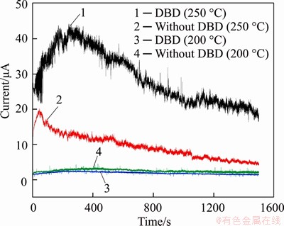
Figure 5 Bonding current of combined system of silicon and glass at bonding temperature of 200 °C, 250 °C with and without DBD
2.4 Tensile strength test
The successfully bonded sample was bonded to the substrate using an epoxy resin as shown in Figure 6. The substrate was fixed on the tensile test stand, and the strength of the sample was tested by stretching the substrate. The tensile strength at the time of fracture of the sample was recorded, and the bonding strength was calculated.
The picture of the fracture sample is shown in Figure 7.
In order to show the advantages of dielectric barrier discharge activation treatment, a comparative experiment was carried out. The first group used milimeter DBD with parameters of 2000 V and 10 kHz, and the second group used nm DBD with parameters of 2000 V and 10 kHz. The third group did not undergo any treatment. After that, the adhesion test was performed at the adhesion temperature of 200, and 250 °C under the adhesion voltage of 2000 V, the adhesion time of 30 min. It can be seen from Figure 8 that the bond strength after nano DBD is the highest.
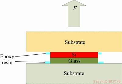
Figure 6 Sample prepared for breaking tests
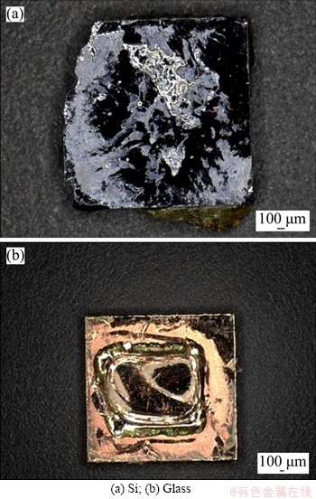
Figure 7 Example of breaking test:
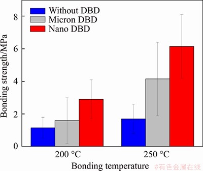
Figure 8 Bonding strength at 200 °C and 250 °C with micron DBD, nano DBD and without DBD
After that, ultra-low temperature anode bonding at 110 °C was performed. Five groups of anode bonding tests without dielectric barrier discharge treatment were performed. The bonding voltage was 2000 V and the bonding time was 30 min. No cases of successful bonding were observed. Multi-parameter tests were performed on the samples after the dielectric barrier discharge activation treatment. As shown in Figure 9, it was found that when the bonding voltage was 3000 V and the bonding time was 30 min, the bonding strength reached 2 MPa. Prolonging the bonding time did not promote the bonding strength obviously.
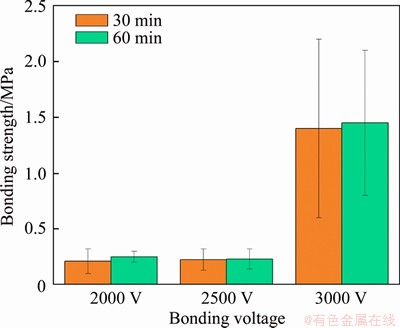
Figure 9 Effect of bonding time on bonding strength at the bonding voltages of 2000, 2500, 3000 V
3 Discussion
Under the action of thermal field and electric field, combined with previous studies [24, 25], two reaction processes occur continuously in the bonding interface region. One is that ions in the glass wafer form an ion depletion layer near the bonding surface under the action of an electric field. The other is that, the physical and chemical reactions occur at the bonding interface. Due to the roughness of the surface, the initial contact of silicon and glass occurs only locally. Almost all of the area of both wafers is separated by a small gap, as indicated by the contact edge at the interface shown in Figure 10. Since the other parts of the glass are electrically conductive, almost all of the voltage drop is concentrated on the resulting depletion layer and this gap. As a result, the electrostatic field is very high and can be in the order of several megavolts per centimeter. Since the attraction of static electricity reaches a maximum at the narrowest point of the gap, that is, the area around the contact point will be subsequently pulled together. In this way, the contact area will extend from the initial contact point to the entire wafer. As shown in Figure 10(b), as the cation moves toward the cathode, a depletion layer is formed, and an interface electrostatic field is formed on the silicon surface and the depletion layer. The generated electrostatic force further pulls the glass to microscopic creep, and the contact point is formed at the silicon glass interface; at the same time, the glass space network is reconstructed due to Na+ motion on the depletion layer, as shown in Figure 10; the O2- ions are transferred to the silicon/glass under the action of their own concentration difference and electrostatic field. The interface diffuses and moves through the interface, and reacts with the silicon surface at the contact position as follows [26]:
Si+2H2O→SiO2+4H++4e (1)
Si+H++[O-Si-OH]-→Si-O-Si+H2O (2)
Si+2O2-→SiO2+4e (3)
At the same time, the water adsorbed at the bonding interface; after the voltage is applied, the water is decomposed into H+ and OH-, and the hydroxyl group is temporarily connected with Si to form an unstable Si(OH)4 complex, which is then decomposed to form more stable SiO2 and water. The specific reaction is as follows [27, 28]:
Si+4[OH]-→Si(OH)4+4e (4)
Si(OH)4→SiO2+2H2O (5)
A chemical reaction occurs at the contact point to form a bonding point, and the position of the contact point is changed in the vicinity of the position, and then the surface of the glass is again micro-peristalous under the action of the electrostatic field, and then bonding occurs, thereby gradually forming the entire surface from the point bonding.
When the bonding temperature is low, the glass does not reach the softening temperature, and is almost non-conductive; the ion movement is very difficult, and the electrostatic force in the gap is very weak. At this time, the bonding surface cannot be approached by electrostatic force, so surface needs to be treated. The energy in the DBD plasma can act on the surface of the material by the collision of light radiation, neutral particle flow and ion current. Therefore, the dissipation process of these energy is the root cause of the modification of the surface of the material. The following three physical and chemical changes occur mainly on the surface of the bonding interface after DBD plasma treatment:
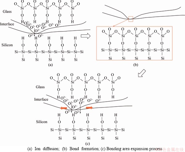
Figure 10 Schematic diagram of interface reaction bonding formation:
1) Generating free radicals: dielectric barrier discharge space active particles impinge on the silicon/glass surface to open the surface intermolecular chemical bonds to generate macromolecular radicals, making the surface of the substrate reactive. Whether it is a reactive gas (such as O2, CO) or a non-reactive gas (such as N2, He), once it is applied for a short time via an applied electric field, a large amount of active particles are generated. The reaction between particles and the surface of the material will generate free radicals.
2) Surface etching occurs: the high-energy particles in the dielectric barrier discharge space bombard the surface of the interface, causing the surface of the material to become rough and the surface shape to change. The etching can remove the weak boundary of the material surface, causing the surface of the material to undulate, roughen, and break with chemical bonds to form free radicals. The etching eventually causes the surface of the material to become rough, and even large bumps appear, increasing the specific surface of the sample.
When θe<90°, the increase in roughness will make the contact angle smaller; when θe>90°, the increase in roughness will make the contact angle larger. This is the basic principle that surface roughening causes a change in hydrophilicity. It is worth noting that the etching time is too long, which will damage the mechanical properties of the material matrix.
3) Introduction of polar groups: the free radicals on the surface of the material and the reactive active particles of the DBD discharge space combine to introduce a polar group having a relatively strong reactivity. It is more common to generate hydroxyl groups or carboxyl groups at the generated radical sites, and to introduce oxygen- containing groups such as —OH, —O on the surface of the silicon/glass.
It is precisely because of the introduction of these reactive polar groups that the activity of the bonding interface surface after DBD plasma treatment is significantly improved, and chemical bonds are more easily formed during the anodic bonding process.
When the silicon glass bonding surface is activated by the DBD discharge plasma in the air, a plurality of active particles formed by the dielectric barrier discharge in the air: high energy electrons, atomic O, ozone (O3), nitrogen oxides (NO and N2O, etc.), neutral particles, metastable particles, free radicals, and ultraviolet rays. These active ions have an energy of 1-10 eV under the action of an electric field. When colliding with the surface of a silicon/glass wafer, the surface of the lens can exist. Si—O bond (key energy about 3.8 eV), H—O bond (key energy about 4.8 eV), H—H bond (key energy about 0.2-0.3 eV), and other chemical bonds open, as shown in Figures 11(b)-(c); large number of active dangling bonds are formed. And more bonding points will be formed at the same bonding voltage, pressure, and temperature as shown in Figure 10(b). And superior to the presence of these active suspensions, reducing the bonding temperature and voltage promotes the chemical bonding of the silicon/glass bonding interface, enabling efficient bonding at lower bonding temperatures. This is the root cause of the activation of the interface to promote low temperature bonding. After activation by this method, the anodic bonding process can be regarded as the fusion of the traditional anodic bonding process and the low-temperature activated anodic bonding process.
It is speculated that when the temperature is 250 °C, at the instant of bonding, the applied voltage is evenly distributed on the glass body. The sodium ions inside the glass move toward the cathode plate of the power supply under the action of the electric field force. The surface is enriched or or is coated with ions, and the bonding current reaches a peak. Due to their poor mobility, the non-bridged oxyanion ions basically do not move and remain in the glass near the anode side, forming a cation depletion layer. In order to maintain the electrical neutrality of the entire bonding system, an equal amount of positive charges are accumulated on the surface of the silicon wafer, and a strong electric field is formed between the bonding interfaces, so the silicon wafer and the glass wafer are in close contact under the action of the electric field force. After the dielectric barrier discharge activation treatment, the bonding current significantly increased because the surface of the material became rough and the surface area increased by the treatment. At the same time, the polar groups attached to the surface reduced the distance between the surfaces and the contact area increased. This leads to an increase in bonding current. When the temperature is as low as 200 °C, it is very difficult for ions to move in the glass. Even if the contact area is increased, the charged particles can hardly move, so the difference in bonding current is not large. At ultra-low temperature of 110 °C, the glass is almost non-conductive, so the voltage is evenly distributed throughout the glass. The electric field applied to the depletion layer and the gap is very small. Therefore, the electrostatic force acting on the surface of the material is very small. The active dangling bonds and polar groups after DBD treatment now replace the role of electrostatic force, making the surface of the material close, and promoting anodic bonding. This process has good compatibility with the anodic bonding process, enabling activation and bonding in a place. It provides a supplement for the low temperature anodic bonding process.
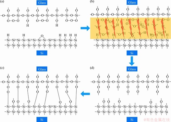
Figure 11 Schematic diagram of effect of discharge plasma on silicon/glass bonding
Contributors
YAO Fu-rong performed the data analysis and wrote the manuscript; PAN Ming-qiang contributed to the conception of the study; ZHU Zong-jian and LIU Ji-zhu made the charts, reviews, and analysis; WANG Yang-jun and PAN Ming-qiang funded the acquisition.
Conflict of interest
YAO Fu-rong, PAN Ming-qiang, ZHU Zong-jian, LIU Ji-zhu, WAAN Yang-jun declare that they have no conflict of interest.
References
[1] WALLIS G, POMERANTZ D I. Field assisted glass-metal sealing [J]. Journal of Applied Physics, 1969, 40: 3946-3949. DOI: 10.1063/1.1657121.
[2] POMERANTZ D I. Anodic bonding: US Pateat, 3397278 [P]. 1968-08-13.
[3] CHEN M X, YI X J, GAN Z Y, LIU S. Reliability of anodically bonded silicon–glass packages [J]. Sensors & Actuators A Physical, 2005, 120(1): 291-295. DOI: 10.1016/j.sna.2004.11.031
[4] LEIB J, GYENGE O, HANSEN U, MAUS S, HAUCK K, ZOSCHKE K, TOEPPER M. Wafer-level glass-caps for advanced optical applications [C]// Proceedings Electronic Components & Technology Conference. Lake Buena Vista, FL: IEEE, 2012: 1642-1648. DOI: 10.1109/ECTC.2011. 5898732.
[5] DASCHNER R, KUBLER H, LOW R, BAUR H, FRUHAUF N, PFAU T. Triple stack glass-to-glass anodic bonding for optogalvanic spectroscopy cells with electrical feedthroughs [J]. Applied Physics Letters, 2014, 105(4). DOI: 10.1063/1.4891534.
[6] LEE H J, KIM Y, YOON E S, CHO I J. Versatile size and shape microlens arrays with high numerical apertures [J]. Journal of Microelectromechanical Systems, 2014, 23(4): 771-773. DOI: 10.1109/jmems.2014.2305993.
[7] YOO S, JIN J Y, HA J G, JI C H, KIM Y K. Two-dimensional optical scanner with monolithically integrated glass microlens [J]. Journal of Micromechanics & Microengineering, 2014, 24(5): 055009. DOI: 10.1088/0960-1317/24/5/055009.
[8] BARGIEL S, GORECKI C, BARANSKI M, PASSILLY N, WIEMER M, JIA C, FROMEL J. 3D micro-optical lens scanner made by multi-wafer bonding technology [J]. Proceedings of Spie the International Society for Optical Engineering, 2013, 8616(4): 5. DOI: 10.1117/ 12.2002422.
[9] SURDO S, MERLO S, CARPIGNANO F, STRAMBINI L M, TRONO C, GIANNETTI A, BALDINI F, BARILLARO G. Optofluidic microsystems with integrated vertical one-dimensional photonic crystals for chemical analysis [J]. Lab on A Chip, 2012, 12(21): 4403-4415. DOI: 10.1039/c2lc40613f.
[10] MHASKAR R, KNAPPE S, KITCHING J. A low-power, high-sensitivity micromachined optical magnetometer [J]. Applied Physics Letters, 2012, 101(83): 241105. DOI: 10.1063/1.4770361.
[11] KOGITA Y, HIRAI Y, TABATA O, TSUCHIYA T. Double-side-drive electrostatic optical chopper for time-resolved Raman spectroscopy [C]// 2014 International Conference on Optical MEMS and Nanophotonics (OMN). IEEE, 2014. DOI: 10.1109/OMN.2014.6924545.
[12] MALEKI T, FOGLE B, ZIAIE B. A batch fabricated capacitive pressure sensor with an integrated Guyton capsule for interstitial fluid pressure measurement [J]. Journal of Micromechanics & Microengineering, 2011, 21(5): 054005. DOI: 10.1088/0960-1317/21/5/054005.
[13] HSU Y W, CHEN J Y, CHIEN H T, CHEN S, LIN S T, LIAO Lu-po. New capacitive low-g triaxial accelerometer with low cross-axis sensitivity [J]. Journal of Micromechanics & Microengineering, 2010, 20(5): 055019. DOI: 10.1088/0960-1317/20/5/055019.
[14] LEE M C, KANG S J, JUNG K D, CHOA S H, CHO Y C. A high yield rate MEMS gyroscope with a packaged SiOG process [J]. Journal of Micromechanics & Microengineering, 2005, 15(11): 2003-2010. DOI: 10.1088/0960-1317/15/ 11/003.
[15] QUESTE S, SALUT R, CLATOT S, RAUCH J Y, KHAN MALEK C G. Manufacture of microfluidic glass chips by deep plasma etching, femtosecond laser ablation, and anodic bonding [J]. Microsystem Technologies, 2010, 16(s8, 9): 1485-1493. DOI: 10.1007/s00542-010-1020-1.
[16] CHANG T H. Electron-beam microcolumns for lithography and related applications [J]. Journal of Vacuum Science & Technology B: Microelectronics & Nanometer Structures, 1996, 14: 3774. DOI: 10.1116/1.588666.
[17] HSIEH G W, TSAI C H, LIN W C. Anodic bonding of glass and silicon wafers with an intermediate silicon nitride film and its application to batch fabrication of SPM tip arrays [J]. Microelectronics Journal, 2005, 36(7): 678-682. DOI: 10.1016/j.mejo.2005.04.057.
[18] WEI J, XIE H, NAI M L, WONG C K, LEE L C. Low temperature wafer anodic bonding [J]. Journal of Micromechanics & Microengineering, 2003, 13(2): 217-222. DOI: 10.1088/ 0960-1317/13/2/308.
[19] YOU Zheng, MA Bo, RUAN Yong, CHEN Shuo, ZHANG Gao-fei. Microfabrication of MEMS alkali metal vapor cells for chip-scale atomic devices [J]. Optics & Precision Engineering, 2013, 21: 1440-1446. DOI: 10.3788/ OPE.20132106.1440. (in Chinese)
[20] DRAGOI V, MITTENDORFER G, THANNER C, LINDNER P Wafer-level plasma activated bonding: New technology for MEMS fabrication [J]. Microsystem Technologies, 2008, 14(4, 5): 509-515. DOI: 10.1007/ s00542-007-0437-7.
[21] CHOI S W, CHOI W B, LEE Y H, JU B K, SUNG M Y, KIM B H. The analysis of oxygen plasma pretreatment for improving anodic bonding [J]. Journal of the Electrochemical Society, 2002, 149(1): G8-G11. DOI: 10.1149/1.1419187.
[22] COOLS P, ASADIAN M, NICOLAUS W, DECLERCQ H, MORENT R, de GEYTER N. Surface treatment of PEOT/PBT (55/45) with a dielectric barrier discharge in air, helium, argon and nitrogen at medium pressure [J]. Materials, 2018, 11(3): 391. DOI: 10.3390/ ma11030391.
[23] MUI T S M, SILVA L L G, PRYSIAZHNYI V, KOSTOV K G. Surface modification of aluminium alloys by atmospheric pressure plasma treatments for enhancement of their adhesion properties [J]. Surface and Coatings Technology, 2017, 312: 32-36. DOI: 10.1016/j.surfcoat.2016.08.024.
[24] WANG Duo-xiao, WU Yu-ting, CHU Jia-ru. Research on low temperature anodic bonding technique [J]. Journal of Transducer Technology, 2005, 24: 37-39. (in Chinese)
[25] KAMAL M R, KALYON D. Heat transfer and microstructure in extrusion blowmolding [J]. Polymer Engineering and Science, 1983, 23(9): 503-509. DOI: 10.1002/pen.760230905.
[26] KIBRIA M G, ZHANG F, LEE T H, KIM M J, HOWLADER M M R. Comprehensive investigation of sequential plasma activated Si/Si bonded interfaces for nano-integration on the wafer scale [J]. Nanotechnology, 2010, 21(13): 134011. DOI: 10.1088/0957-4484/21/13/ 134011.
[27] HOWLADER M M R, ZHANG F. Void-free strong bonding of surface activated silicon wafers from room temperature to annealing at 600 °C [J]. Thin Solid Films, 2010, 519(2): 804-808. DOI: 10.1016/j.tsf.2010.08.144.
[28] HOWLADER M M R, KIBRIA M G, ZHANG F, KIM M J. Hybrid plasma bonding for void-free strong bonded interface of silicon/glass at 200 °C [J]. Talanta, 2010, 82(2): 508-515. DOI: 10.1016/ j.talanta.2010.05.001.
(Edited by HE Yun-bin)
中文导读
基于纳米间隙介质阻挡放电的硅与玻璃超低温阳极键合
摘要:本文对介质阻挡放电(DBD)活化阳极键合工艺进行了改进。通过亲水性表面测试来表征处理后的表面,结果表明纳米间隙条件下亲水角明显降低并得到最优的放电电压为2 kV。然后,进行了阳极键合与介质阻挡放电活化键合的对比试验,通过拉伸破坏测试来表征键合强度,结果表明纳米间隙下活化键合强度更高。完成了110 °C低温下的阳极键合,键合强度为2 MPa。最后讨论了活化后促进键合的机理。
关键词:介质阻挡放电;阳极键合;超低温度
Foundation item: Project(6140863020216JW30001) supported by the General Armaments Department Pre-research Fund, China
Received date: 2020-01-13; Accepted date: 2020-11-22
Corresponding author: PAN Ming-qiang, PhD, Associate Professor; Tel: +86-15862305976; E-mail: pmqwl@126.com; ORCID: https:// orcid.org/0000-0002-3909-4396

