
Atomic diffusion properties in wire bonding
LI Jun-hui(李军辉), WANG Fu-liang(王福亮), HAN Lei(韩 雷), DUAN Ji-an(段吉安), ZHONG Jue(钟 掘)
College of Mechanical-Electronical Engineering, Central South University, Changsha 410083, China
Received 10 May 2005; accepted 28 December 2005
Abstract: The lift-off characteristics at the interface of thermosonic bond were observed by using scanning electron microscope (JSM-6360LV). The vertical section of bonding point was produced by punching, grinding and ion-sputter thinning, and was tested by using transmission electron microscope (F30). The results show that the atomic diffusion at the bonded interface appears. The thickness of Au/Al interface characterized by atomic diffusion is about 500 nm under ultrasonic and thermal energy. The fracture morphology of lift-off interface is dimples. The tensile fracture appears by pull-test not in bonded interface but in basis material, and the bonded strength at interface is enhanced by diffused atom from the other side.
Key words: thermosonic bond; atomic diffusion; dimples, bonding strength
1 Introduction
Ultrasonic bonding was applied primarily to wire bonding in microelectronic packaging industry, while the mechanism of ultrasonic bonding has not been understood very well. Harman[1] observed that the peeling underdeveloped bonds simulate a torus (or doughnut) with an unbonded central region and ridged peripheral region is bonded hardly by using SEM. The same phenomena in thermosonic flip chip took place [2,3]. The effects of the power, time, and load on the features of the bond interface were researched by VERN et al[4]. For constant force and time, the ridged area of the bond pattern increases when more power applied. For constant force and power, the ridged location of the bonded region moves closer to the bond center with time. For constant power and time, the total area of bond pattern increases in size with increasing load.
To research mechanism of thermosonic bonding, the temperature of aluminum wedge bonding process was 200-300 ℃ tested by Tsujino et al[5,6] through measuring thermoelectromotive force voltage between aluminum wire and substrate. The interfacial temperature rise during gold wire ball bonding was not that high (70- 80 ℃) tested by using real-time temperature monitoring systems with 6 μm thermocouples by Suman et al[7] and Mayer et al[8]. Intuitive friction weld idea is unreasonable.
The elastic modulus of aluminum is reduced substantially when the acoustic energy is applied during a tensile testing[9]. Such softening of metal under the influence of high-level acoustic radiation occurs in all of the materials studied (including aluminum, cadmium, beryllium, steel, zinc, copper, iron and gold)[10-15]. However, ‘acoustic-plastic effect’ has been elusive and there are much debate in physics.
In this paper, atomic diffusion in vertical section of ultrasonic bonding process was tested by using TEM with EDS, and lift-off cracking at interface was observed with scanning electron microscope.
2 Experimental
Nickel-pad plated on a copper plate was bonded using 500 μm diameter-aluminum wire and LW500 wedge capillary on a U3000 ultrasonic wire wedge bonder. Aluminum-pad in chip was bonded using 18 μm diameter-gold wire and WT051A ball capillary on a T/S-2100 ultrasonic wire bonder.
Atomic diffusion of vertical section was tested by using high resolution TEM (F30) with line scanning EDS-test whose beam is 10 nm, and fracture morphology of bonding was researched by using SEM (JSM- 6360LV).
3 Results and discussion
3.1 Atomic diffusion
For Au/Al bonded vertical section under conditions of power 1.75 W, bonding time 35 ms, load 0.76 N, and temperature 200 ℃ on T/S-2100 Au ball bonder, Fig.1 shows that atomic diffusion at the bonded Au/Al interface appears. The line 1-1 in Fig.1 is the line scanning location. The thickness of Au/Al interface is about 500 nm under ultrasonic and heating energy. EDS-testing data at atomic diffusion point are listed in Table 1. Table 1 shows that there is an intermetallic compound (e.g. Au4Al).
The intermetallic compounds at interface are mostly brittle and have lower conductivity, and can decrease the mechanic-electronical performance. The intermetallic compounds must be controlled by the bonding processes as decreasingly as possible.
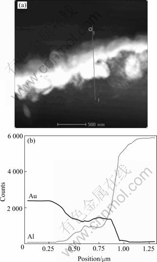
Fig. 1 Result of EDS-test with line scanning on vertical section of Au/Al bonding by using STEM model
Table 1 Result of EDS-test at atomic diffusion point

The velocity of vibration at wedge capillary was tested by using PSV-400-M2 high frequency (1.5 MHz)
laser doppler vibrometer. For power in U3000 wedge bonder being 8 W, the result of vibration velocity at the end of wedge capillary is shown in Fig.2. The beginning of vibration under piezodectric transducer(PZT) driven by the high frequency is nonlinear phase. When vibrating stably, the peak value of vibration velocity is A=2.2 m/s. Fig.3 shows the expanding curve for the result of vibration velocity in 20-20.1 ms in Fig.2. The result shows that the vibration is sinusoid and can be written as
v(t)=Asin(ωt+φ) (1)
where ω is frequency, and φ is phase.
Fig.4 shows the result of Fast Fourier Transform (FFT) from Fig.2. The result shows that the vibrating frequency is f=58.06 kHz. So,
ω=2πf=2×3.14×58.06×103=3.65×10⁵ (2)
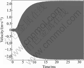
Fig.2 Result of vibration velocity at wedge capillary
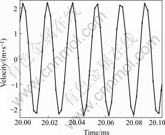
Fig.3 Expanding graph for result of vibration velocity in 20- 20.1ms
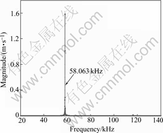
Fig.4 FFT for result of vibration velocity at wedge capillary
The acceleration of ultrasonic vibration is

The peak value of vibration acceleration is

It is shown that the acceleration of ultrasonic vibration tested is about 80 000 times as the acceleration of gravity for 58.06 kHz bonding capillary by using PSV-400-M2 high frequency laser vibromter. The strong mechanical effect activates dislocations at metal crystal lattice and increases atomic diffusibility, and softens materials, simultaneously cleans brittle oxides and contaminations in welding interface and reveals clean surface. Thus atom bonding at interface is formed by ultrasonic energy.
3.2 Break characteristics in lift-off interface
Fig.5 shows the lift off characteristics at bonded interface in Al/Ni. Fig.6 shows the break characteristics at point A in Fig.5. The results indicate that the peeling underdeveloped wedge bonds simulate a torus (or doughnut) with an unbonded central region and ridged peripheral region is bonded hardly. Dimples are formed, tensile fracture appears not in bonded interface but in basis material, and real break is in base material or weak places.
Figs.7 and 8 show the break characteristics in lift-off Au ball bond interface. The results shows that central region in ball bonding interface is bonded hardly, and lift-off break is dimple fracture too, and is in base material or weakness.
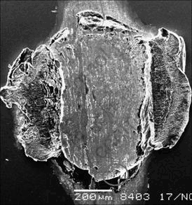
Fig.5 SEM image of lift off characteristics at bonded interface in Al/Ni
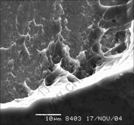
Fig.6 SEM image of lift off characteristics at point A in Fig.5
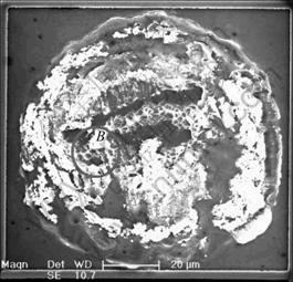
Fig.7 SEM image of lift off characteristics at bonded interface in Au/Al
The diffused atoms enhance the microstructure strength, which is higher than strength of the base material.
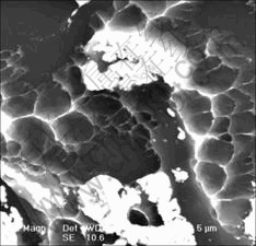
Fig.8 SEM image of lift off characteristics at point B in Fig.7
4 Conclusions
1) In very short time that was the order of millisecond, Atoms of bonding materials on the bonding interface are diffused. The thickness of atomic diffusion layer is about 500 nm.
2) The diffused atoms enhanced the microstructure strength, which was higher than strength of the basis material. Bonded strength was formed by atomic diffusion. Break characteristics were dimples, tensile fracture appeared not in bonded interface but in basis material or weak places.
References
[1] Harman G G. The ultrasonic welding mechanism as applied to aluminum- and gold-wire bonding in microelectronics[J]. IEEE Transactions on Packaging, 1997, 13(4): 406-415.
[2] LI Jun-hui, HAN Lei, ZHONG Jue. Microstructure characteristics at the thermosonic bond interface[J]. China Mechanical Engineering, 2005, 16(4): 341-344. (in Chinese)
[3] LI Jun-hui, HAN Lei, ZHONG Jue. The characteristics of ultrasonic vibration transmission and coupling in bonding technology[A]. The Sixth IEEE CPMT Conference on High Density Microsystem Design and Packaging and Component Failure Analysis (HDP'04)[C]. Shanghai, China, 2004. 311-315.
[4] Vern H, Wnchell I, Howard B. Enhancing ultrasonic bond development[J]. IEEE Transactions on Manufacturing Technology, 1998, 1(3): 211-220.
[5] Tsujino J, Yoshihara H, Sano T, IHARA S. High-frequency ultrasonic wire bonding systems[J]. Ultrasonics, 2000, 38(3): 77-80.
[6] Tsujino J, Yoshihara H, Kamimoto K, OSADA Y. Welding characteristics and temperature rise of high frequency and complex vibration ultrasonic wire bonding [J]. Ultrasonics, 2002, 36(2): 59-65.
[7] Suman S, Joshi Y, Harman G G, et al. Wire bond temperature sensor[J]. National Institute of Standards and Technology, 2002, 1: 5-14.
[8] Mayer M, Paul O, Bolliger D. Integrated temperature microsensors for characterization and optimization of thermosonic ball bonding process[A]. Proceedings of the 1999 Electronic Components and Technology(ECTC) [C]. California: San Diego, 1999. 463-468.
[9] Kang S Y, Williams P M, Lee Y C. Modeling and experiment studies on thermosonic flip chip bonding [J]. IEEE Trans on Components, Packaging, and Manufacturing Technology, 1995, 18(4): 728-733.
[10] Peter E, Lee L. Comparing flip-chip and wire-bond interconnection technologies[J]. IEEE Transactions on Packaging, 2000(8): 81-87.
[11] Tan Q, Schaible B, Leonard J, LEE Y C. Thermosonic flip chip with a self-planarization feature using polymer[J]. IEEE Trans on Components, Packaging, and Manufacturing Technology, 1998, 19(5): 1-8.
[12] McLaren T S, Kang S Y, Zhang W, LEE Y C. Thermosonic bonding of an optical transcever based on 8x8 cavity surface emitting laser array[J]. IEEE Trans on Components, Packaging, and Manufacturing Technology-Part B, 1997, 20(2): 152-160.
[13] Kang S Y, Williams P M, McLaren T S, LEE Y C. Studies of thermosonic bonding for flip-chip assembly[J]. Materials Chemistry and Physics, 1995(42): 31-37.
[14] Maruo H, Seki Y, Unami Y. Development of ultrasonic flip chip bonding for flexible printed circuit [A]. The Sixth IEEE CPMT Conference on High Density Microsystem Design and Packaging and Component Failure Analysis (HDP'04)[C]. Shanghai, China, 2004. 307-310.
[15] KAJIWARA R. Ultrasonic flip chip bonding technology for LSI chip with high pin counts[A]. The Seventh Symposium on Microjoining and Assembly Technology in Electrocs[C]. Yokohama, 2001. 161- 166.
Foundation item: Projects(50390064; 50575229; 50575230) supported by the National Natural Science Foundation of China; Project(2003CB716202) supported by the National Basic Research Program of China
Corresponding author: LI Jun-hui; Tel: +86-731-8877842; E-mail: lijunhui@mail.csu.edu.cn
(Edited by YUAN Sai-qian)

