
J. Cent. South Univ. (2018) 25: 2332-2338
DOI: https://doi.org/10.1007/s11771-018-3917-2

Effect of capacitance on ZnO-Bi2O3-Yb2O3 based varistor for nanosecond transients
Kannadasan RAJU, Valsalal PRASAD
Department of Electrical & Electronics Engineering, CEG Campus, Anna University, Chennai, India
 Central South University Press and Springer-Verlag GmbH Germany, part of Springer Nature 2018
Abstract: The microstructure and electrical properties of ZnO-Bi2O3-Yb2O3 based varistor ceramics were investigated with various temperature effects from 900 ��C to 1050 ��C. From the results, it was observed that the increase of sintering temperature offers a reduced capacitive effect from 0.460 nF to 0.321 nF. Furthermore, the grain sizes of varistors were varied from 6.8 ��m to 9.8 ��m. The consequence of such smaller grain sizes provided a better voltage gradient of about 895 V/mm for the disc sintered at 900 ��C and fallen drastically to 410 V/mm for the sample sintered at 1050 ��C. In addition, there was an increase of non-linearity index to a maximum value of 36.0 and reduced leakage current of 0.026 mA/cm2. However, the density of the varistor decreased with an increase of temperature from 5.41 g/cm3 to 5.24 g/cm3. With this base, the influence of varistor capacitance and high voltage gradient were scrutinized and it led an improved transition speed of the varistor assembly from non-conduction to conduction mode during intruding nanosecond transients.
Key words: capacitance; metal oxide varistor; nanosecond transient; rare earth oxide; transition delay; ytterbium oxide
Cite this article as: Kannadasan RAJU, Valsalal PRASAD. Effect of capacitance on ZnO-Bi2O3-Yb2O3 based varistor for nanosecond transients [J]. Journal of Central South University, 2018, 25(10): 2332�C2338. DOI: https://doi.org/ 10.1007/s11771-018-3917-2.
1 Introduction
Metal oxide (ZnO) varistors are predominantly used to protect the electric circuit in both low and high voltage applications against surges. They are connected between the line and ground, their primary role is to divert the surge current to ground and clamp the voltage within limited value [1].These phenomena occur by mean of high non-linear V�CI characteristics of varistor ceramics. They offer insulating (non-conductive) properties beneath a breakdown field and highly nonlinear properties (conductive) beyond the breakdown field. On the other hand, the polycrystalline pure ZnO offers ohmic properties i.e., the current is directly proportional to the voltage. In order to obtain nonohmic behavior, ZnO varistors are fabricated by adding a small fraction of Bi2O3, Sb2O3, Cr2O3 etc. [2�C6]. Moreover, this nonlinear behavior decides the clamping voltage across the varistor and discharge current through it. In continuation of this, the successful operation of the arrester is warranted with the attainment of clamping voltage peak with respect to the current transients. For instance, incoming transients with front time greater than 1 ��s results a voltage attain peak before current peak and thereby varistor conduct the surge successfully [7�C11]. This occurrence is due to the fast disappearance of varistor capacitance and so potential breakdown happens quickly to clamp the voltage before current takes a peak.
Moreover, VALSALAL et al [7] described that the current transients with a front time less than 1 ��s causes a delay in initial response of the varistor due to the attainment of voltage peak after the current peak. The very fast transients (<1 ��s) not allow the capacitance (during non-conduction) to disappear quickly. Therefore, a delay occurs to change from non-conduction to conduction mode (failure in potential breakdown). In order to accomplish successful conduction of varistor against these fast (nanosecond) transients, it is crucial to decrease the time lag between the peak of clamping voltage and current (delay time). Some of the possible measures to improve the initial response of the varistor are obtaining higher voltage gradient, higher non-linearity and reducing varistor capacitance [7, 9, 11].
Furthermore, the addition of rare earth oxide with varistor composition decreases the average grain size effectively. There are many rare earth oxides which influence the varistor behavior [12]. It consequences high voltage gradient and so the length of the varistor blocks reduces noticeably [13, 14] for high voltage applications. Hence, ZnO- Bi2O3-Yb2O3 based varistor was developed experimentally to get appropriate electrical behavior against nanosecond transient. In order to study the dynamic behavior of developed varistor against nanosecond surges, a simulation study is a viable option and the required electrical parameters for arrester model is computed and simulated against various current surges.
2 Experiment
The varistor samples were prepared using high grade raw materials in the proportion of 96.3 at%ZnO+0.7 at at% Bi2O3+1.0 at%Sb2O3+0.8 at% Co2O3+0.5 at% MnO2+0.5 at% Cr2O3+0.2 at% Yb2O3. The weighed raw materials were milled by high-energy ball mill with zirconia balls and acetone as a wetting agent. The ball mill was allowed to run for 5 h at a speed of 300 r/min. The milled powders were dried at 120 ��C for 24 h and calcined in air at 600 ��C for 2 h. The calcined powders were pulverized using agate mortar after adding a 2 wt% of PVA (Poly Vinyl Alcohol). The granulation of pulverized powders was made by sieving through 150 ��m mesh screen to avoid lumps in staring powder. The powders were filled into a cylindrical die, placed between the arms of the uniaxial pressing machine and pressed with a pressure of 100 MPa. The pressed pellets were sintered at different temperatures such as 900 ��C, 950 ��C, 1000 ��C and 1050 ��C for 2 h in an air atmosphere and cooled at furnace temperature. The sintered varistors are labeled as V1, V2, V3 and V4 with respect to their sintering temperatures from 900 ��C to 1050 ��C. The heating and cooling rates were maintained at 5 ��C/min. The final dimension of the samples was achieved by grinding machine. In order to investigate the electrical behavior of the prepared samples, the conductive silver paste was applied on both faces of the disc and heated at 500 ��C for 10 min.
3 Results and discussion
3.1 Microstructure properties
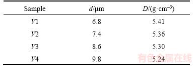
The surface microstructural analysis was made by scanning electron microscope (SEM, Tescan- Vega 3) and shown in Figure 1. From SEM images, it is established that the Bi-rich and contents of Yb2O3 are formed as secondary phases between the grains. The small variations of grain sizes are found between the samples because of increasing temperature. But with the influence of ytterbium oxide, grain growth was restricted to some extent due to larger ionic radii of the rare earth compared to ZnO which offer a strong pinning effect during sintering [15]. Consequently, the average grain sizes of varistors are limited and these may result in a higher varistor voltage to accomplish compact varistor blocks [16]. The average grain size (d) was determined by linear intercept method using the formula d=1.56 L/(MN), where L is the length of random lines, M is the magnification of micrograph and N is the number of grains intercepted by the random lines. The calculated value of average grain sizes of different samples is shown in Table 1. It shows that the grain size increases with the increase in temperature.
The relative densities (D) of different varistor samples are also given in Table 1. It shows that the densities of sintered samples are changing with the different sintering effects. This is due to the presence of Bi2O3 which volatizes during higher temperature and lowers the relative density of the ZnO-Bi2O3-Yb2O3 varistor. Therefore, the sample V1 results in a higher density of 5.41 g/cm3. Further increase of temperature reduces the density considerably to a value about 5.24 g/cm3.
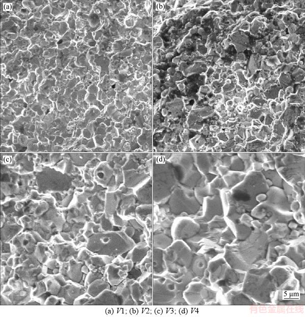
Figure 1 SEM images of samples:
Table 1 Microstructural properties of all prepared samples
3.2 Electrical properties
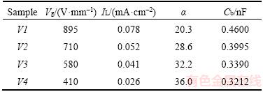
The electrical properties of the varistors were found using high voltage DC source unit. The V�CI characteristics of the sintered samples are shown in Figure 2. It is found that the sample V4 shows a sharper knee between two modes (insulation to conduction) which pronounces the better nonlinear properties. Moreover, the energy handling capability of the varistor strongly depend on the position of the upturn region and it is decided by the resistivity of ZnO. The sharper knee shows the better resistivity and this may lead to minimizing the failure of the varistor disc during transients. From the V�CI characteristics, the breakdown voltage (Vb) of all samples were observed at a current density of 1.0 mA/cm2. The voltage gradients (Vg) were derived from Vb/t, where ��t�� is the thickness of the varistor (1 mm). The leakage currents (IL) were determined from 0.75Vb. The nonlinear coefficients (��) were derived from the current densities of 1.0 mA/cm2 and 10 mA/cm2. The capacitances of varistor blocks (Cb) were determined using impedance analyzer (Wayne B). Table 2 shows the computed electrical parameters of all prepared samples.
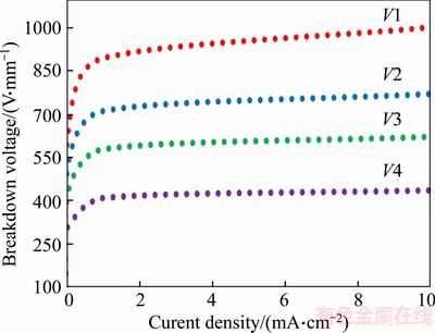
Figure 2 V�CI Characteristics of varistor samples
Table 2 Electrical properties of all prepared samples
The voltage gradient (Vg) shows variance between the sample and V1 gives a higher voltage gradient of about 895 V/mm. Moreover, the breakdown voltage is directly proportional to the number of grain boundaries between the electrodes. Therefore, a decrease in grain size can linearly increase the number of grains between the electrodes. This leads to the increase of voltage gradient noticeably. Additionally, this high voltage gradient can improve the conduction behavior (transition speed from non-conduction to conduction) of varistor blocks due to the reduction of stray capacitance (capacitive effect with respect to ground) which decreases with reduction in height of varistor.
During non-conduction mode, the varistor behaves as a capacitor and it needs a certain time to turn on from non-conduction mode (capacitive) to conduction mode (ohmic) because of the strong capacitive effect. The impact of this capacitive effect on varistor operation depends on the steepness of the incoming transients [7, 9]. This shows the fact that the high steep transients do not allow the capacitance to disappear quickly and result in a delay in the potential breakdown.
The effect of stray capacitance (Cs) increases with the height of varistor arrangement with respect to their voltage rating. The higher voltage gradient of varistor block condenses height requirement and so the Cs effect decreases extensively. Consequently, fastness of transition from non-conduction to conduction mode even with high steepness transients. Moreover, the higher voltage gradient concedes a more compact design of arrester assembly for higher voltage applications.
The nonlinear coefficient (��) of samples increases from 20.3 to 36.0 with an increase of temperature as shown in Table 2. The variation of �� is directly associated with the Schottky height of barrier and hence small variation of doping concentration and sintering affects the nonlinear property of the varistor significantly. Additionally, it is found that the leakage current (IL) decreases with the increase of temperature from 0.078 mA/cm2 to 0.026 mA/cm2. Therefore, the lifespan of the varistors increases extensively.
VALSALAL et al [7] reported that the effect of Cb during nanosecond transient results a time lag (delay of varistor response) between the peaks of clamping voltage and current transient. It is also justified that the reduction of Cb in the varistor block leads to the increase the arrester response.Table 2 shows the capacitance of varistor blocks (Cb) for all samples and V4 gives Cb of 0.3212 nF which is least compared with other samples. The variation of Cs and Cb between the samples are plotted in per unit and shown in Figure 3.
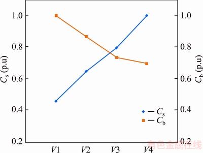
Figure 3 Relationship between Cs and Cb
The sample with higher voltage gradient provides lesser Cs compared with conventional varistor for the given rating. Hence, the increased voltage gradient of samples is inversely proportional to the stray capacitive effect. Therefore, the sample V1 gives less Cs effect compared with other samples. On the other hand, the value of Cb for sample V4 is less and increases towards the sample V1. The combined effect of Cs and Cb is responsible for the delay in varistor operation.
4 Dynamic behavior of varistor assembly
A 198 kV varistor assembly is considered for further studies with simulation platform (using modified IEEE arrester model) [17]. In order to accomplish the required arrester voltage rating, a number of varistor blocks are stacked in series.
The nanosecond current transient with a peak of 500 A and front time (tf: time taken to reach its peak) of 5 ns is considered for simulation study and shown in Figure 4. In order to divert the current transient through varistor and ground, a complete potential breakdown happens as quickly as possible. On contrary, the capacitive effect does not allow the varistor to make a complete potential breakdown during the injection of nanosecond transient [17�C19]. Therefore, the clamping voltage takes a peak with a delay against given current transient. In other words, the varistor behaves as pure capacitor during the non-conduction mode. During invading of transients, the capacitance has to diminish quickly without any delay to turn on varistor into ohmic (from non-conduction to conduction) and diverts the nanosecond current transient to ground.
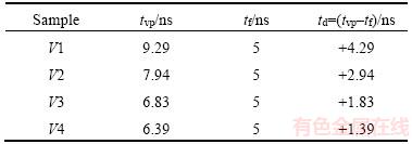
The clamping voltages of all prepared samples are simulated against nanosecond transient (peak: 500 A, tf : 5 ns, indicated in Figure 4 separately) and observed plots are given in Figure 5. It is noticed that the voltage fails to attain peak faster than current peak due to the capacitive effect and cause a delay in transition. The delay (td) is the difference between the time taken to reach the peak of clamping voltage (tvp) and tf.
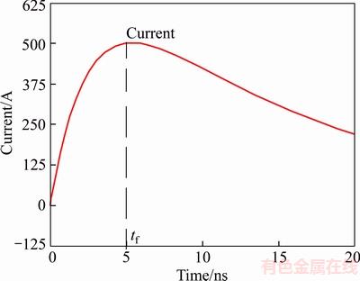
Figure 4 Current transient used for simulation
The delay must be zero or negative for the successful disappearance of capacitive effect (successful diversion of transient to ground).Table 3 shows the ranges of td for all varistor samples. Among the four samples, the capacitive effect of V4 vanishes quickly, i.e., the value of td decreases noticeably (+1.39) which ensures the improvement in the fastness of transition speed from capacitive to resistive. However, it is essential to nullify the delay for successful varistor operation.
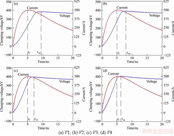
Figure 5 Behavior of various arrester assemblies for nanosecond transients:
Table 3 Value of tvp and td for different samples with tf= 5ns
5 Conclusions
The microstructure and electrical properties of ZnO-Bi2O3-Yb2O3 based varistors have been investigated with different sintering effects of 900 ��C (V1), 950 ��C (V2), 1000 ��C (V3) and 1050 ��C (V4). Among these samples, V4 gives a least leakage current of 0.026 mA/cm2, the higher nonlinear coefficient of 36.0, the high voltage gradient of 410 V/mm and lesser varistor block capacitance of 0.0321 nF. Moreover, the dynamic behavior of developed samples is studied using simulation against nanosecond transients. It shows that the sample V4 gives a lesser time delay with improved transition speed of varistor from non-conduction to conduction mode during invading of nanosecond transients. In order to obtain successful arrester operation, the delay must be nullified. This can be achieved with different compositions and advanced processing methods and it will be discussed in future work.
References
[1] NAHM Choon-woo. Sintering effect on ageing behavior of rare earths (Pr6O11-Er2O3-Y2O3)-doped ZnO varistor ceramics [J]. Journal of Rare Earth, 2012, 30(10): 1028�C1033.
[2] XU Dong, SHI Xiao-feng, CHENG Xiao-nong, YANG Juan, FAN Yue-e, YUAN Hong-ming, SHI Li-yi. Microstructure and electrical properties of Lu2O3-doped ZnO-Bi2O3-based varistor ceramics [J]. Transactions of Nonferrous Metals Society of China, 2010, 20(12): 2303�C2308.
[3] XU Dong, TANG Dong-mei, LIN Yuan-hua, JIAO Lei, ZHAO Guo-ping, CHENG Xiao-nong. Influence of Yb2O3 doping on microstructural and electrical properties of ZnO-Bi2O3-based varistor ceramics [J]. Journal of Central South University, 2012, 19: 1497-1502.
[4] XU Dong, TANG Dong-mei, LIN Yuan-hua, JIAO Lei, ZHAO Guo-ping CHENG Xiao-nong. Microstructure and electrical properties of Er2O3-Doped ZnO-Based varistor ceramics prepared by high-energy ball milling [J]. Journal of Rare Earth, 2007, 25: 120-123.
[5] kE Lei, YUAN Yan-hong, ZHAO Hua, MA Xue-ming. Influence of rare-earth doping on the electrical properties of high voltage gradient ZnO varistors [J]. Ceramics-Silik��ty, 2013, 57(1): 53-57.
[6] BAI Hai-rui, LI Shu-hui, ZHAO Yun-han, XU Zhi-jun, CHU Rui-qing, HAO Ji-gong, CHEN Chong, LI Huai-yong, GONG Yun-yun, LI Guo-rong. Influence of of Cr2O3 on highly nonlinear properties and low leakage current of ZnO-Bi2O3 varistor ceramics [J]. Ceramic International, 2016, 42(9): 10547�C10550.
[7] VALSALAL P, USA S, UDAYAKUMAR K. Response of metal oxide arrester in gas-insulated substation and methods to improve its dynamic characteristics [J]. IET Science Measurement & Technology, 2012, 6(2): 222�C228.
[8] VALSALAL P, USA S, UDAYAKUMAR K. Importance of capacitance on metal oxide arrester block model for VFTO applications [J]. IEEE Transactions on Power Delivery, 2011, 26(2): 1294�C1295.
[9] VALSALAL P, USA S, UDAYAKUMAR K. Modelling of metal oxide arrester for very fast transients [J]. IET Science Measurement & Technology, 2011, 5(4): 140�C146.
[10] PRASAD V. Possible measures to enhance the performance of Metal�COxide arresters in the EHV network under very fast transients [J]. IEEE Transactions on Power Delivery, 2015, 30(2): 783�C790.
[11] CHEN Jie, GUO Jie, QIU Ai-ci, LI Ke-lun, XIE Yan-zhao, CUI Long-yue, WANG Lei, CHEN Zhi-qiang. Behavior comparison of metal oxide Arrester blocks when excited by VFTO and lightning [J]. IEEE Transactions on Electromagnetic Compatibility, 2015, 57(6): 1608�C1615.
[12] XU Dong, WU Jie-ting, JIAO Lei, XU Hong-xing, ZHANG Pei-mei, YU Ren-hong, CHENG Xiao-nong. Highly nonlinear property and threshold voltage of Sc2O3 doped ZnO-Bi2O3-based varistor ceramics [J]. Journal of Rare Earth, 2013, 31(2): 158�C163.
[13] HE Jin-liang, LIU Jun, HU Jun, LONG Wang-cheng. AC ageing characteristics of Y2O3-doped ZnO varistors with high voltage gradient [J]. Materials Letters, 2011, 20(12): 2595�C2597.
[14] SHICHIMIYA S, YAMAGUCHI M, FURUSE N, KOBAYASHI M, ISHIBE S. Development of advanced arresters for GIS with new zinc-oxide elements [J]. IEEE Transactions on Power Delivery, 1998, 13(2): 465�C471.
[15] HE Jin-liang, HU Jun, LIN Yuan-hua. ZnO varistors with high voltage gradient and low leakage current by doping rare-earth oxide [J]. Science in China Series E: Technological Sciences, 2008, 51(6): 693�C701.
[16] NAHM Choon-woo. Nonlinear behavior of Tb4O7-modified ZnO-Pr6O11-based ceramics with high breakdown field [J]. Journal of Rare Earth, 2013, 31(3): 273�C280.
[17] RAJU K, PRASAD V, RAMASAMY J. Performance improvement of metal oxide arrester for very fast transients [J]. IET Science Measurement & Technology, 2017, 11(4): 438�C444.
[18] RAJU K, PRASAD V, RAMASAMY J. High gradient metal oxide surge arrester block for VFTO applications [J]. Journal of Electrical Engineering, 2017, 17(1): 411�C417.
[19] RAJU K, PRASAD V, RAMASAMY J. Development of metal oxide arrester block using rare earth element for very fast transient overvoltage applications [J]. Turkish Journal of Electrical Engineering and Computer Sciences, 2017, 25: 4893�C4900. DOI: 10.3906/elk-1611-56, 2017.
(Edited by HE Yun-bin)
���ĵ���
���ݶԺ���˲����ZnO-Bi2O3-Yb2O3��ѹ�������Ӱ��
ժҪ���о���ZnO-Bi2O3-Yb2O3��ѹ���մ���900 ��C��1050 ��C�¶ȷ�Χ�ڵ�����֯�͵�ѧ���ܱ仯����������������ս��¶ȵ����ߣ�����ЧӦ��0.460 nF���͵�0.321 nF�����⣬ѹ������ľ�����С��6.8 ��m����9.8 ��m������С�ľ���ʹ��Ʒ��900 ��C�ս�ʱ��ø��õĵ�ѹ�ݶȣ�ԼΪ895 V/mm�������ս��¶����ߵ�1050 ��Cʱ����ѹ�ݶ�Ѹ���½���410 V/mm�����⣬������ָ�����ӵ����ֵ36.0��й©�������ٵ�0.026 mA/cm2��Ȼ���������¶ȵ����ߣ�ѹ��������ܶȴ�5.41 g/cm3���͵�5.24 g/cm3���ڴ˻����ϣ�������ѹ��������ݺ�ѹ�ݶȵ�Ӱ�죬�Ӷ������ѹ�������������������˲̬�´ӷǵ���̬ת�䵽����̬��ת���ٶȡ�
�ؼ��ʣ����ݣ�����������ѹ�����裻����˲̬��ϡ�������ת���ӳ٣�������
Received date: 2017-07-15; Accepted date: 2017-10-21
Corresponding author: Kannadasan RAJU, PhD; Tel: +91-9600137705; E-mail: kannan.3333@yahoo.co.in; ORCID: 0000-0001-7622- 8261

