������ѹ��AlN��Ĥ���ṹ��������ѧ���ܵ�Ӱ��
��Դ�ڿ����й���ɫ����ѧ��(Ӣ�İ�)2014���9��
�������ߣ�κ��ƽ ����ΰ ������ �� �� �ܿƳ� �� �� ��־��
����ҳ�룺2845 - 2855
Key words��AlN thin film; reactive magnetron sputtering; preferred orientation; nanomechanical properties
ժ Ҫ���о��ڲ�ͬ��ѹ�£�������Ƶ�ſؽ��䷨��Si(100)�ϳ���������(AlN)��Ĥ����ʹ��XRD��SEM��AFM��XPS������ѹ�۵ȱ����ֶ��о���Ĥ�����ʡ�XRD����������ڵ�ѹ�������ڳ���c��ȡ��ı�Ĥ�����ڸ���ѹ��������(100)���������SEM��AFM���������������ѹ�����ߣ��������ʺͱ���ֲڶȾ���С������ֲڶ������ӡ�XPS���������������ѹ�����ڼ��ٱ�Ĥ�е����������Ӷ�ʹ�Ʊ��ı�Ĥ�ɷָ��ӽ��仯ѧ�����ȡ�ͨ������AlN��Ĥ��������ѧ���ܱ�������0.30 Pa���Ʊ��ı�Ĥ��������Ӳ�Ⱥ͵���ģ����
Abstract: Wurtzite aluminum nitride (AlN) films were deposited on Si(100) wafers under various sputtering pressures by radio-frequency (RF) reactive magnetron sputtering. The film properties were investigated by XRD, SEM, AFM, XPS and nanoindenter techniques. It is suggested from the XRD patterns that highly c-axis oriented films grow preferentially at low pressures and the growth of (100) planes are preferred at higher pressures. The SEM and AFM images both reveal that the deposition rate and the surface roughness decrease while the average grain size increases with increasing the sputtering pressure. XPS results show that lowering the sputtering pressure is a useful way to minimize the incorporation of oxygen atoms into the AlN films and hence a film with closer stoichiometric composition is obtained. From the measurement of nanomechanical properties of AlN thin films, the largest hardness and elastic modulus are obtained at 0.30 Pa.
Trans. Nonferrous Met. Soc. China 24(2014) 2845-2855
Qiu-ping WEI1,2, Xiong-wei ZHANG2, Dan-ying LIU2, Jie LI1, Ke-chao ZHOU3, Dou ZHANG3, Zhi-ming YU2,3
1. School of Metallurgy and Environment, Central South University, Changsha 410083, China;
2. School of Materials Science and Engineering, Central South University, Changsha 410083, China;
3. State Key Laboratory of Powder Metallurgy, Central South University, Changsha 410083, China
Received 8 October 2013; accepted 3 April 2014
Abstract: Wurtzite aluminum nitride (AlN) films were deposited on Si(100) wafers under various sputtering pressures by radio-frequency (RF) reactive magnetron sputtering. The film properties were investigated by XRD, SEM, AFM, XPS and nanoindenter techniques. It is suggested from the XRD patterns that highly c-axis oriented films grow preferentially at low pressures and the growth of (100) planes are preferred at higher pressures. The SEM and AFM images both reveal that the deposition rate and the surface roughness decrease while the average grain size increases with increasing the sputtering pressure. XPS results show that lowering the sputtering pressure is a useful way to minimize the incorporation of oxygen atoms into the AlN films and hence a film with closer stoichiometric composition is obtained. From the measurement of nanomechanical properties of AlN thin films, the largest hardness and elastic modulus are obtained at 0.30 Pa.
Key words: AlN thin film; reactive magnetron sputtering; preferred orientation; nanomechanical properties
1 Introduction
The wurtzite aluminum nitride (AlN) films with wurtzite hexagonal structure have attracted increasing attention for their exceptional properties such as high thermal conductivity (285 W/mK at room temperature) [1,2], wide band-gap width (6.2 eV) [3], fine piezoelectric activity, high wave speed and high electromechanical coupling factor [4]. AlN is an excellent candidate for gigahertz surface acoustic wave (SAW) devices [5], bulk acoustic wave (BAW) devices [6-8] and LED [9].
At present, AlN thin films can be prepared by various kinds of techniques, such as chemical vapor deposition [10], pulsed laser deposition [11], molecular beam epitaxy [12] and magnetron sputtering [13-15]. Compared with other techniques, reactive magnetron sputtering owns many advantages like low deposition temperature, low cost, easy to control the experiment parameters, which lead to their wide use. The key lies on controlling the parameters so as to effectively regulate their micro-structure, which determines the properties of AlN thin films.
In this work, hexagon structure AlN thin films with different orientations were deposited on silicon (100) substrate by RF magnetron sputtering techniques. We set a series of experiments by adjusting the sputtering parameters, so as to investigate the correlations among chemical composition, crystal structure, surface morphology, thickness and nanomechanical properties. Nowadays, much attention has been paid to nanomechanical property of AlN. Since AlN thin film needs to be applied in various electronic devices, it is necessary to investigate its mechanical properties besides optical and electrical properties. Furthermore, the properties of these devices might be seriously impaired due to the micro loading during machining, packaging and utilizing. FIGUEROA et al [16] revealed the influence of sputtering pressure on hardness of AlN thin film deposited on glass substrate. They thought that the changes of residual stress and its effect on hardness and fracture properties are mainly affected by the columnar growth and thickness of thin film. And OLIVEIRA et al [17] found that the substrate temperature and the sort of working gas greatly influence the hardness of AlN thin film, while preferred orientation has less effect on the hardness. However, research on nanomechanical properties of AlN thin films is still seldom reported. It is of great importance in finding the correlation among sputtering pressure, components, structure and nanomechanical property.
2 Experimental
AlN thin films were fabricated by CSU550-I ultra high vacuum magnetron device. The aluminum target was 60 mm in diameter and 4 mm in thickness with a purity of 99.999%. The sputtering and reactive gases were high-purity Ar (99.999%) and N2 (99.999%), respectively. Si(100) wafer with 10 mm��10 mm��0.5 mm in dimensions was used as substrate. And the surfaces of films deposited were mirror polished. Degreasing was carried out in ultrasonic baths of acetone, ethanol and deionized water for 30 min, respectively. The native oxide on the Si wafer was removed through etching in 5% HF solution for 10 s. The sputtering power was kept at 200 W. Distance between the target and the substrate was 30 mm. The chamber was evacuated below 1.8��10-3 Pa, and a mixture of Ar and N2 (flux ratio 1:1) was introduced into. After pre-sputtering, the AlN thin films were deposited at 0.20, 0.30 and 0.55 Pa for 1 h, respectively. Since the substrate was not heated, its temperature was below 150 ��C. The deposition parameters are summarized in Table 1.
The crystal structure and preferred orientation of the thin films were characterized by X-ray diffraction (XRD, Dmax-2500VBX with a Cu K�� radiation source (l=0.154 nm)). An atomic force microscope (AFM NT-MDT, Solver P47) was used to analyze the surface morphology of thin films and roughness. The cross-section morphologies and thickness of the AlN films were observed by a scanning electron microscope (Quanta200 Environmental SEM). An X-ray photoelectron spectrometer (K-Alpha 1063, Thermo Fisher Scientific Ltd.) was applied to analyzing the sort of elements, contents and electronic valence. The data of hardness and modulus of elasticity were collected from nanoindentation tester (CSM Switzerland, UNHT).
3 Results and discussion
3.1 Structural analysis
Figure 1 shows the XRD patterns of the AlN thin films deposited under different pressures. The intensity of AlN (002) peak in the thin film is much stronger than that of AlN (100) under the pressure of 0.20 Pa, indicating a fine c-axis preferred orientation. Increasing the pressure to 0.30 Pa, both the (100) and (002) peaks of AlN appear in the pattern. For the sample prepared at 0.55 Pa, (100) peak of AlN turns out to be the strongest and that of AlN (002) weakens a lot. Remarkably, the peak of AlN (100) is much sharper than that of AlN (002) at 0.30 Pa, indicating that this film has better crystallinity.
As it can be seen above, the sputtering pressure has significant influence on the preferred orientation of AlN thin film. Increasing the pressure is beneficial to the growth of (100) plane while (002) plane grows preferentially at a relatively low sputtering pressure. During sputtering, the longer mean free path (��) of particles at a low sputtering pressure lowers the possibility of particles colliding with each other, thus keeping particle energy at a high level, which results in high nucleation density and deposition rate. All these conditions are suitable for the growth of (002) preferred orientation [18]. On the contrary, increasing the sputtering pressure reduces �� of particles and increases the possibility of collision between sputtering particles and Ar ions, which will lead to much more scattering and make the energy level and number of sputtering particles reaching the substrate diminish drastically. Therefore, the deposition rate and the nucleation density both decrease, which is good for the growth of (100) preferred orientation. Besides, at high pressures, Al atoms sputtered from the target and activated nitrogen atoms could form Al-N clusters through once or several times of collision and then were deposited on the substrate, which enhanced the growth of (100) plane [19-21].
Table 2 shows the structural parameters of AlN thin films deposited under different sputtering pressures. And we calculated the interplanar distance and crystal size of all samples by Bragg equation and Scherrer formula.
Table 1 Deposition parameters of AlN thin films

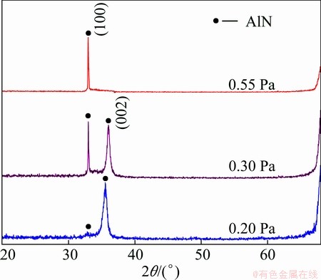
Fig. 1 XRD spectra of AlN thin films deposited under different pressures
Table 2 Structural parameters of AlN thin films deposited under different sputtering pressures
It can be seen from Table 2 that crystal size grows along the ascent of sputtering pressure. At low pressures, the atomic clusters sputtered from the target own low possibility of colliding with gas ions on their way to the substrate and the diffraction of sputtered clusters (Al, N, Al-N and etc.) is small. Therefore, there is a large quantity of atomic clusters flying to the substrate surface. Their kinetic energy and mobility are kept at high levels. But they are soon covered by subsequent atomic groups before migration, which inhibits the growth of crystal. While at high pressures, the sputtering atomic groups have more chances to collide with gas particles, which reduces the number and kinetic energy of atomic groups reaching the substrate and lowers their mobility. Studies have shown that it presents a polymerization effect [22] in order to reduce the total surface energy among fine grains. The reduction of diffusion energy will lead to the enhancement of polymerization among fine grains. Furthermore, since less particles fly to the surface of substrate, the atomic groups after condensation have much time to grow via diffusion migration and coalesce with the nearest neighbor atomic groups. These factors above are conducive to the further growth of grains.
Observed from Table 2, as the gas pressure increases from 0.20 Pa to 0.55 Pa, the ratio of the intensity to full width half maximum (I/FWHM) of (002) plane and (100) plane gradually increases. The I/FWHM value of (100) plane is larger than that of (002) plane at 0.30 Pa.
3.2 Deposition rate
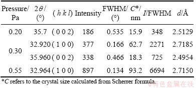
Figure 2 shows the cross-sectional SEM images of the AlN thin films deposited under different sputtering pressures. The thickness of film first increases and then decreases with the ascent of sputtering pressure, which indicates that the deposition rate of film first increases and then decreases. The deposition rates of AlN thin films are 22.2, 24.7 and 12.6 nm/min at 0.20, 0.30 and 0.55 Pa, respectively.
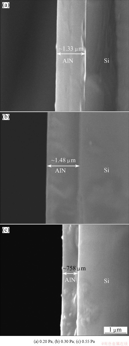
Fig. 2 Cross-sectional SEM image of AlN thin films deposited under different pressures
CHENG et al [18] considered that the sputtering pressure can affect deposition rate positively and negatively. On one hand, the collision between the electrons and gas molecules increases with increasing the sputtering pressure, resulting in the enhancement of gas ionization and increasing the density of Ar+ and so on, so that the ions bombard the target more frequently, which helps increasing the sputtering rate of the target and deposition rate. On the other hand, as the pressure increases, the possibility of collision between atomic clusters from the target and gas ions also increases and the chance of particles arriving at the substrate reduces. This results in the reduction of deposition rate of thin film. It is the combined effects of these two factors that cause the deposition rate to first increase and then decrease in our experiment.
3.3 Morphologic analysis
Figure 3 shows the AFM images of AlN thin films deposited under different sputtering pressures. The film deposited under the pressure of 0.20 Pa shows a uniform and dense morphology with circular columnar grains of (002) preferred orientation. As the pressure increases to 0.30 Pa, grains turn into various shapes and their boundaries become unclear. A few of small grains start to agglomerate. At 0.55 Pa, the grain shape turns to be silkworm-like and the film has comparatively large pores. It can be clearly seen that the majority of silkworm-like grains are parallel to the substrate surface. The thin film has (100) preferred orientation and its c-axis is parallel to the surface of substrate.
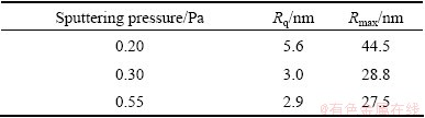
Table 3 shows the influence of sputtering pressure on the roughness of AlN thin films, where Rq refers to the root mean square roughness and Rmax represents the difference in height between the highest and lowest points within the detection range. As the sputtering pressure increases from 0.20 Pa to 0.55 Pa, the roughness of film decreases from 5.6 nm to 2.9 nm; also the Rmax value gradually decreases from 44.5 nm to 27.5 nm. The root mean square roughness of the films is much smaller than 30 nm which meets the requirement of SAW devices [23].
Fig. 3 AFM images of AlN thin films deposited under different pressures
Table 3 Effects of sputtering pressure on roughness of AlN thin film
To explain the effect of pressure on the surface roughness of film, we can adopt the theory that combines the changes of the kinetic energy and the surface migration energy of absorbed atoms during the process of deposition [14]. At low sputtering pressures, the kinetic energy of absorbed atoms on the surface is high, but the deposition rate is high as well, which decreases the diffusion time of Al and N atoms on the substrate surface. Therefore, it is conducive to enhance the crystallization of the film and lower its roughness. The deposition rate gets lower while increasing the sputtering pressure, which means that the Al and N atoms have more time to diffuse on the substrate and results in a rougher surface.
3.4 Film composition analysis
Figure 4 shows the XPS spectra of the AlN thin films deposited under different sputtering pressures without etching or after Ar+ etching for 10 min. The surface of as-deposited AlN thin film is composed of Al, N, O, and C.
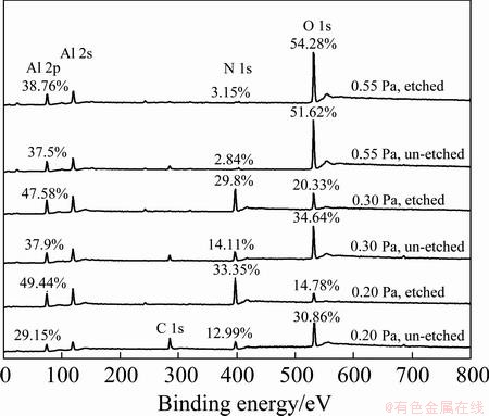
Fig. 4 XPS spectra of AlN thin films deposited under different pressures without etching or etching for 10 min
Figure 5 shows the effects of the sputtering pressure on the mole fractions of Al, N, O and C in the AlN thin film. The aluminum content is higher than that of nitrogen, which indicates that the thin films are Al-rich. Besides, the content of every element in all samples changes a lot after etching. After etching for 10 min, the content of Al or N increases and that of carbon decreases. The contents of O at 0.20 Pa and 0.30 Pa sharply decrease after etching. Only at 0.55 Pa, it increases from 51.62% to 54.28%. This indicates that the pollution of O and C mainly presents in the surface layer of the AlN films, which is caused by surface oxidation after deposition. Since the specimens were only etched for 10 min, the oxygen content of the film is still high. However, referring to Ref. [24] on the analysis of XPS along the depth in AlN thin films, it can be inferred that the oxide layer on the surface will basically be removed if etching for a long time enough, and the measured composition will be closer to the stoichiometric ratio of AlN.
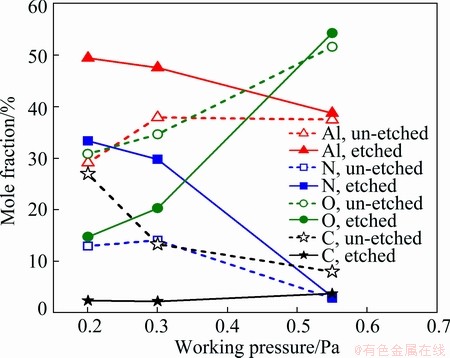
Fig. 5 Effect of sputtering pressure on mole fraction of Al, N, O and C in AlN thin films
Figure 5 demonstrates the content change of each element with sputtering pressure, which is obtained by calculating the area of each peak. The sputtering pressure has great impact on the content of all elements in the AlN thin film. For specimens without etching, the content of oxygen gradually increases from 30.86% to 54.28% when the pressure increases. And the content of N and Al first increases and then decreases. However, the content of C gradually decreases from 27% to 8%. For the films after etching, as the sputtering pressure increases, both the contents of Al and N gradually reduce, while the oxygen content increases; the aluminum content reduces from 49.44% to 38.76%, nitrogen reduces from 33.35% to 3.15% and the oxygen increases from 14.78% to 54.28%. This phenomenon is consistent with that report by LEE et al [25] and PENZA et al [26]. Whether being etched or not, the oxygen content increases with the ascent of sputtering pressure, and excellent anti-oxidation property and high purity are shown by the film prepared under low pressures. ABABNEH et al [27] also found that the content of oxygen is less than 5% at 0.20 Pa, while it increases to 10% at 0.60 Pa. With the increase of sputtering pressure, the content of oxygen in the film is increased, which is due to the strong affinity between aluminum and oxygen atoms [27].
In view of thermodynamics, Al prefers to react with O2 when the contents of N2 and O2 are in the same level at room temperature [25]. Therefore, the sputtered Al atoms react with residue oxygen in the chamber, which causes the formation of alumina. When exposed to the air, it is also easy to form Al2O3 on the surface of the Al-rich thin film. Combined with the XRD analysis above, we can draw a further deduction that the thickness of Al2O3 layer is very thin or it is amorphous. The oxygen content in the film is mainly derived from the residual gas in the chamber. At low pressures, the ion bombardment on the as-deposited film is strong. The oxygen incorporated into the AlN thin film is less due to the decrease of adhesion coefficient of oxygen at low pressures. While increasing the pressure to 0.30 Pa, the deposition rate is higher. High deposition rate can also reduce the content of oxygen derived from residue gas in the chamber. Actually, only 5% of oxygen in the film will hinder its growth along the c-axis. Al2O3 impedes the growth of AlN columnar grains and causes damage to its c-axis preferred orientation [28]. This is consistent with the XRD result, which shows that the preferred orientation gradually changes from (002) to (100) as the concentration of oxygen increases.
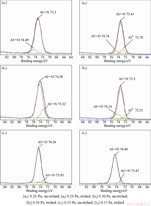
Fig. 6 Al2p XPS spectra of AlN thin films deposited under different pressures before and after etching
The mole ratios of Al to N of as-deposited thin films are 1:0.67, 1:0.63 and 1:0.08 at 0.20 Pa, 0.30 Pa and 0.55 Pa, respectively, after etching for 10 min. The results show that the composition of thin film at 0.20 Pa is the closest to 1:1, which is the stoichiometric value of AlN.
Figure 6 shows the XPS spectra of Al 2p of the AlN thin films prepared under different pressures before and after etching. The binding energy of Al 2p in the metallic state is between 72.5 eV and 72.8 eV, in aluminum nitride it is between 73.1 eV and 74.7 eV and in the aluminum oxide it is between 74.0 eV and 75.6 eV [28]. Before etching, the Al 2p peaks are composed of Al��N bonds and Al��O bonds in all samples. At 0.20 Pa, the Al��N peak is strong and the Al��O peak is weak, indicating that there is little alumina on its surface. In the Al 2p spectra of samples surfaces at 0.30 Pa and 0.55 Pa without etching, the Al��O bond is the main peak and the Al��N bond peak is very weak. This shows that the surface contains more alumina than that at 0.20 Pa. In the Al 2p diagram after etching, the Al 2p peaks at 0.20 Pa and 0.30 Pa are composed of Al��N, Al��O and metallic aluminum after fitting. The Al��N peak is the main peak, while the Al��O and metallic aluminum peaks are weak, indicating that the alumina content is largely reduced after etching. This may be due to the ion induced decomposition of aluminum nitride during the etching process [29]. The Al 2p diagrams of specimen at 0.55 Pa before and after etching are only composed of Al��O bond and Al��N bond. And the peak area of Al��O is much higher than that of Al��N bond, which shows that its surface contains much alumina.
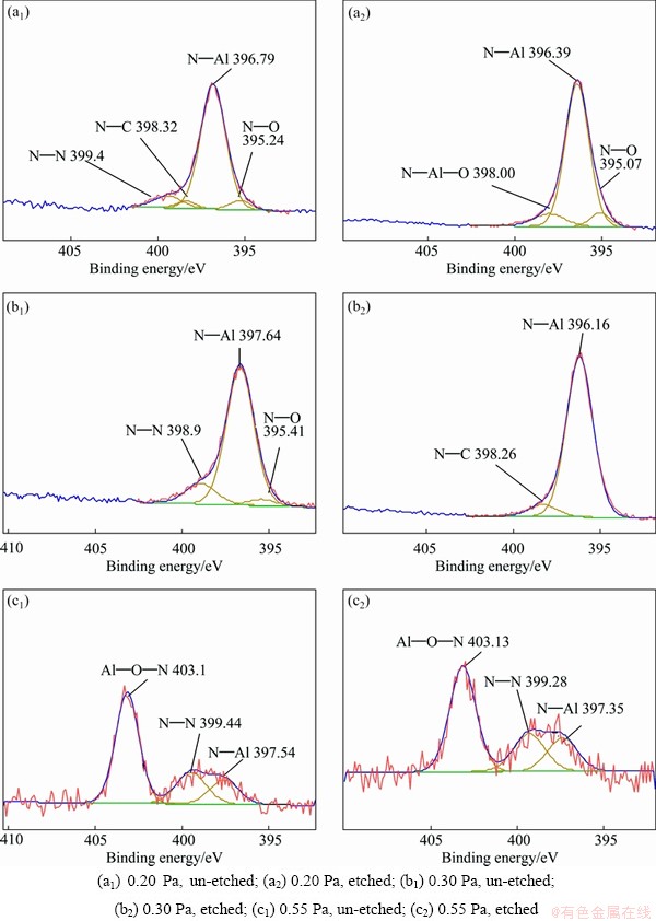
Fig. 7 N1s XPS spectra of AlN thin films deposited under different pressures before and after etching
Figure 7 shows the XPS spectra of N1s in AlN thin films deposited under different pressures. The binding energy of N-Al in the AlN thin films is in the range of 396.16-397.54 eV, confirming the formation of the AlN. It was reported that the binding energy of N��O in the N1s is 395.4 eV [24,30-35] and 395.9 eV [34]. Its formation comes from the oxide layer on the surface of the film [36]. The binding energies of N��C bond are 398.5 eV and 399.5 eV, which exists as nitride and imides in a triple bond or a double bond [34]. The N��N bond comes from the thin film or absorbed N2 molecules, and its binding energy is 399.0-399.6 eV [37].
In the N1s spectra of specimens at 0.20 Pa and 0.30 Pa before etching, N��Al bond is the main peak in the AlN thin film and the peaks of N��C, N��O and N��N bond are very weak. After etching, the peak of N��Al bond is still the main peak on the fitting patterns, but N��N disappears. There are N��O bond and N��Al��O bond [32] in the etched specimen at 0.20 Pa, corresponding to the oxygen content of 14.78% in the film. The above analysis shows that the main constituent of thin films at 0.20 Pa and 0.30 Pa is AlN and a small amount of nitrogen oxide and alumina exist. Also the films have absorbed a few N2 molecules. The N 1s spectrum of sample at 0.55 Pa after fitting consists of three peaks before and after etching. They are Al��O��N bond [32] at 403 eV, N��N bond at 399.28 eV and N��Al bond at 397.54 eV and 397.35 eV. Among them, the peak of Al��O��N bond is the strongest and the N��N peak and the N��Al peak are weak. This shows that there are many oxides on the surface. The surface also has absorbed N2 molecules. The Al��O��N bond at 403.1 eV is formed at the interface of Al2O3 and AlN [38].
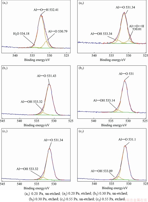
Fig. 8 O 1s XPS spectra of AlN thin films deposited under different pressures before and after etching
Figure 8 shows the O 1s of XPS spectra in the AlN thin films prepared under different pressures before and after etching. At 0.20 Pa, the main peak of O 1s on the surface without etching locates at 532.4 1eV, corresponding to the O 1s of OH-(Al��OH bond), the other two peaks locate at 530.79 eV and 534.18 eV, respectively, corresponding to the O2-(Al��O bond) and the physical absorption of H2O [39]. This demonstrates that the surface mainly consists of Al(OH)3, aluminum oxide and absorbed water. After etching, the main peak of the O 1s spectrum locates at 531.34 eV, the Al��O bond. The binding energy of Al��O bond is 531.15- 531.6 eV [31]. Another two peaks are at 530.01 eV and 533.34 eV, respectively, corresponding to the oxygen in the Al��O��N [30-32,35,37] and Al��OH [32]. After etching, the O 1s of absorbed water disappears and the intensity of peak representing the Al��OH is also greatly reduced. For samples prepared at 0.30 Pa and 0.55 Pa, the O 1s is composed of Al��O and Al��OH, corresponding to aluminum oxide and Al (OH)3 before and after etching. And the main peak is Al��O bond; the peak area of Al��OH is weak, indicating that the content of Al (OH)3 on the surface is much lower than that of alumina.
3.5 Nanomechanics performance analysis
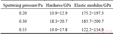
Figure 9 shows the correlation among nano- indentation hardness and elastic modulus and indentation depth of AlN thin films deposited under different pressures. For samples prepared at 0.20 Pa, its hardness is 10.9-12.9 GPa at the depth of 36-80 nm; and its elastic modulus lies between 175.2 GPa and 197.3 GPa. As the sputtering pressure goes to 0.30 Pa, the hardness of thin film increases to 18.3-20.7 GPa at the depth of 33-44 nm, and its elastic modulus is between 185.7 GPa and 200.7 GPa. At 0.55 Pa, hardness of thin film lies between 10.0 and 17.8 GPa at the depth of 24-61 nm and the elastic modulus is in the range of 122.7-154.9 GPa. With the increase of indentation depth, the micro-hardness of thin films gradually decreases, which is close to the substrate hardness. The deformation zone of indentation will extend to substrate if indentation penetration is too deep, thereby making the measured hardness value lower. Based on this, it is recommended that the ratio of indentation depth to film thickness should be less than 1/10-1/20 in order to guarantee its accuracy [40,41].
As it can be seen from the Fig. 9 and Table 4, the hardness and elastic modulus of AlN thin films first increase and then decrease with the increase of pressure. At 0.30 Pa, they reach the maximum. Since the anisotropic generally exists in crystal, different crystal planes possess different mechanical properties. The elastic constant of AlN is anisotropic [42]. The results of XRD and AFM both reveal that the crystal orientation, the grain size and film thickness of each AlN films are not the same in this work. Therefore, the nanomechenical properties of the AlN thin films are relevant to the microstructure, preferred orientation, grain size and other factors.
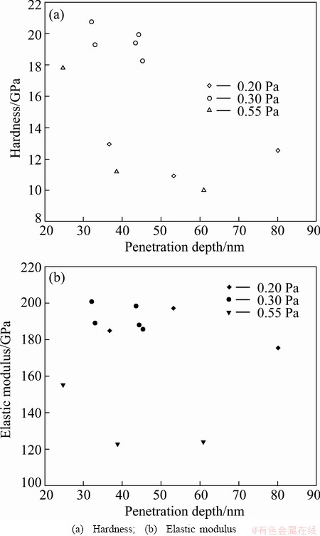
Fig. 9 Mechanical properties of AlN thin films deposited under different sputtering pressures
Table 4 Hardness and elastic modulus of AlN thin films deposited under different sputtering pressures
4 Conclusions
1) It is easy to deposit high c-axis oriented AlN thin films at low pressures, while at high pressures, it is easy to prepare AlN thin films with (100) preferred orientation.
2) With the increase of sputtering pressure, the film deposition rate and surface roughness are gradually reduced, and the grain size is gradually increased.
3) Depositing at low pressures prevents the thin films from being polluted by oxygen, so that the composition of the thin films is close to the stoichiometric composition of the AlN film, thereby enhancing the oxidation resistance of the AlN thin film.
4) Sputtering pressure has great influence on the hardness of AlN thin film. At 0.30 Pa, the hardness and elastic modulus reach the maximum.
References
[1] SLACK G A, TANZILLI R A, POHL R O, VANDERSANDE J W. The intrinsic thermal conductivity of AIN [J]. Journal of Physics and Chemistry of Solids, 1987, 48: 641-647.
[2] YIN Tao-tao, YANG Bao-he, LI Cui-ping, WANG Jin. Preparation and piezoelectric properties of (100) oriented AlN film [J]. Journal of Optoelectronics Laser, 2012, 23: 1327-1332. (in Chinese)
[3] LUO J T, ZHU X Y, CHEN G, ZENG F, PAN F. The electrical, optical and magnetic properties of Si-doped ZnO films [J]. Applied Surface Science, 2012, 258: 2177-2181.
[4] LUO J T, ZENG F, PAN F, LI H F, NIU J B, JIA R, LIU M. Filtering performance improvement in V-doped ZnO/diamond surface acoustic wave filters [J]. Applied Surface Science, 2010, 256: 3081-3085.
[5] LUO J T, LUO P X, XIE M, DU K, ZHAO B X, PAN F, et al. A new type of glucose biosensor based on surface acoustic wave resonator using Mn-doped ZnO multilayer structure [J]. Biosensors & Bioelectronics, 2013, 49: 512-518.
[6] RODRIGUEZ-MADRID J G, IRIARTE G F, PEDROS J, WILLIAMS O A, BRINK D, CALLE F. Super-high-frequency saw resonators on AlN/Diamond [J]. IEEE Electron Device Lett, 2012, 33: 495-497.
[7] CALIENDO C. Gigahertz-band electroacoustic devices based on AlN thick films sputtered on Al2O3 at low temperature [J]. Appl Phys Lett, 2003, 83: 4851-4853.
[8] CALIENDO C, IMPERATORI P. High-frequency, high-sensitivity acoustic sensor implemented on AlN/Si substrate [J]. Appl Phys Lett, 2003, 83: 1641-1643.
[9] TANIYASU Y, KASU M. Surface 210 nm light emission from an AlN p-n junction light-emitting diode enhanced by A-plane growth orientation [J]. Appl Phys Lett, 2010, 96: 221110.
[10] TIAN W, YAN W Y, DAI J N, LI S L, TIAN Y, XIONG H, ZHANG J B, FANG Y Y, WU Z H, CHEN C Q. Effect of growth temperature of an AlN intermediate layer on the growth mode of AlN grown by MOCVD [J]. Journal of Physics D: Applied Physics, 2013, 46: 065303.
[11] WANG Z P, MORIMOTO A, KAWAE T, ITO H, MASUGATA K. Growth of preferentially-oriented AlN films on amorphous substrate by pulsed laser deposition [J]. Phys Lett A, 2011, 375: 3007-3011.
[12] BENAISSA M,  P, TOTTEREAU O, NGUYEN L, SEMOND F. Investigation of AlN films grown by molecular beam epitaxy on vicinal Si (111) as templates for GaN quantum dots [J]. Appl Phys Lett, 2006, 89: 231903.
[13] KALE A, BRUSA R S, MIOTELLO A. Structural and electrical properties of AlN films deposited using reactive RF magnetron sputtering for solar concentrator application [J]. Applied Surface Science, 2012, 258: 3450-3454.
[14] KUANG X P, ZHANG H Y, WANG G G, CUI L, ZHU C, JIN L, SUN R, HAN J C. AlN films prepared on 6H�CSiC substrates under various sputtering pressures by RF reactive magnetron sputtering [J]. Applied Surface Science, 2012, 263: 62-68.
[15] LIU H Y, TANG G S, ZENG F, PAN F. Influence of sputtering parameters on structures and residual stress of AlN films deposited by DC reactive magnetron sputtering at room temperature [J]. Journal of Crystal Growth, 2013, 363: 80-85.
[16] FIGUEROA U, SALAS O, OSEGUERA J. Process-microstructure- properties relationship during formation of AlN layers by physical vapour deposition [J]. Surf Eng, 2006, 22: 109-120.
[17] OLIVEIRA I C, GRIGOROV K G, MACIEL H S, MASSI M, OTANI C. High textured AlN thin films grown by RF magnetron sputtering; composition, structure, morphology and hardness [J]. Vacuum, 2004, 75: 331-338.
[18] CHENG H E, LIN T C, CHEN W C. Preparation of [002] oriented AlN thin films by mid frequency reactive sputtering technique [J]. Thin Solid Films, 2003, 425: 85-89.
[19] CHENG H, SUN Y, HING P. The influence of deposition conditions on structure and morphology of aluminum nitride films deposited by radio frequency reactive sputtering [J]. Thin Solid Films, 2003, 434: 112-120.
[20] IRIARTE G F, ENGELMARK F, KATARDJIEV L. Reactive sputter deposition of highly oriented AIN films at room temperature [J]. J Mater Res, 2002, 17: 1469-1475.
[21] KHANNA A, BHAT D G. Effects of deposition parameters on the structure of AlN coatings grown by reactive magnetron sputtering [J]. J Vac Sci Technol A, 2007, 25: 557-565.
[22] XU X H, WU H S, ZHANG C J, JIN Z H. Morphological properties of AlN piezoelectric thin films deposited by DC reactive magnetron sputtering [J]. Thin Solid Films, 2001, 388: 62-67.
[23] YANG D, JONNALAGADDA R, ROGERS B R, HILLMAN J T, FOSTER R F, CALE T S. Texture and surface roughness of PRCVD aluminum films [J]. Thin Solid Films, 1998, 332: 312-318.
[24] WANG C C, CHIU M C, SHIAO M H, SHIEU F S. Characterization of AlN thin films prepared by unbalanced magnetron sputtering [J]. J Electrochem Soc, 2004, 151: F252-F256.
[25] LEE H C, KIM G H, HONG S K, LEE K Y, YONG Y J, CHUN C H, et al. Influence of sputtering pressure on the microstructure evolution of AlN thin films prepared by reactive sputtering [J]. Thin Solid Films, 1995, 261: 148-153.
[26] PENZA M, de RICCARDIS M F, MIRENGHI L, TAGLIENTE M A, VERONA E. Low temperature growth of r.f. reactively planar magnetron-sputtered AlN films [J]. Thin Solid Films, 1995, 259: 154-162.
[27] ABABNEH A, SCHMID U, HERNANDO J, SANCHEZ-ROJAS J L, SEIDEL H. The influence of sputter deposition parameters on piezoelectric and mechanical properties of AlN thin films [J]. Mater Sci Eng B, 2010, 172: 253-258.
[28] IRIARTE G F, RODRIGUEZ J G, CALLE F. Synthesis of c-axis oriented AlN thin films on different substrates: A review [J]. Materials Research Bulletin, 2010, 45: 1039-1045.
[29] GARCIA-MENDEZ M, MORALES-RODRIGUEZ S, SHAJI S, KRISHNAN B, BARTOLO-PEREZ P. Structural properties of aln films with oxygen content deposited by reactive magnetron sputtering: XRD and XPS characterization [J]. Surf Rev Lett, 2011, 18: 23-31.
[30] KUANG X P, ZHANG H Y, WANG G G, CUI L, ZHU C, JIN L, SUN R, HAN J C. Effect of deposition temperature on the microstructure and surface morphology of c-axis oriented AlN films deposited on sapphire substrate by RF reactive magnetron sputtering [J]. Superlattice Microst, 2012, 52: 931-940.
[31] LAIDANI N, VANZETTI L, ANDERLE M, BASILLAIS A, BOULMER-LEBORGNE C, PERRIERE J. Chemical structure of films grown by AlN laser ablation: An X-ray photoelectron spectroscopy study [J]. Surface and Coatings Technology, 1999, 122: 242-246.
[32] OZGIT C, DONMEZ I, ALEVLI M, BIYIKLI N. Self-limiting low-temperature growth of crystalline AlN thin films by plasma-enhanced atomic layer deposition [J]. Thin Solid Films, 2012, 520: 2750-2755.
[33] DUEZ N, MUTEL B, DESSAUX O, GOUDMAND P, GRIMBLOT J. AlN formation by direct nitrogen implantation using a DECR plasma [J]. Surface and Coatings Technology, 2000, 125: 79-83.
[34] MANOVA D, DIMITROVA V, KARPUZOV D, YANKOV R. REACTIVELY D C. magnetron sputtered thin AlN films studied by X-ray photoelectron spectroscopy and polarised infrared reflection [J]. Vacuum, 1999, 52: 301-305.
[35] ISHIHARA M, YUMOTO H, TSUCHIYA T, AKASHI K. Effect of bias voltage on A1N thin films prepared by electron shower method [J]. Thin Solid Films, 1996, 281-282: 321-323.
[36] MANOVA D, DIMITROVA V, FUKAREK W, KARPUZOV D. Investigation of d.c.-reactive magnetron-sputtered AlN thin films by electron microprobe analysis, X-ray photoelectron spectroscopy and polarised infra-red reflection [J]. Surface and Coatings Technology, 1998, 106: 205-208.
[37] MAHMOOD A, MACHORRO R, MUHL S, HEIRAS J,  ANDRADE E. Optical and surface analysis of DC-reactive sputtered AlN films [J]. Diamond and Related Materials, 2003, 12: 1315-1321.
[38] PARK J Y, NO Y S, PARK B J, LEE H W, CHOI J W, KIM J S, ERMAKOV Y, YOON S J, OH Y J, CHOI W K. Low-energy ion beam treatment of ��-Al2O3(0001) and improvement of photoluminescence of ZnO thin films [J]. Met Mater-Int, 2004, 10: 351-355.
[39] WANG P S, MALGHAN S G, HSU S M. The oxidation of an aluminum nitride powder studied by bremsstrahlung-excited Auger electron spectroscopy and X-ray photoelectron spectroscopy [J]. J Mater Res, 1995, 10: 302-305.
[40] CAMMARATA R, SCHLESINGER T, KIM C, QADRI S, EDELSTEIN A. Nanoindentation study of the mechanical properties of copper-nickel multilayered thin films [J]. Appl Phys Lett, 1990, 56: 1862-1864.
[41] LLOYD S, CASTELLERO A, GIULIANI F, LONG Y, MCLAUGHLIN K, MOLINA-ALDAREGUIA J M, STELMASHENKO N A, VANDEPERRE L J, CLEGG W J. Observations of nanoindents via cross-sectional transmission electron microscopy: A survey of deformation mechanisms [J]. Proceedings of the Royal Society A: Mathematical, Physical and Engineering Science, 2005, 461: 2521-2543.
[42] WAGNER C D, RIGGS W M, MOULDER L E, MUILENBERG G E. Handbook of X-ray photoelectron spectroscopy: A reference book of standard spectra for identification and interpretation of XPS data [M]. Eden Prairie: Perkin-Elmer Corporation Electronics Division, 1995.
κ��ƽ1,2������ΰ2��������2���� ��1���ܿƳ�3���� ��3����־��2,3
1. ���ϴ�ѧ ұ���뻷��ѧԺ����ɳ 410083��
2. ���ϴ�ѧ ���Ͽ�ѧ�빤��ѧԺ����ɳ 410083��
3. ���ϴ�ѧ ��ĩұ������ص�ʵ���ң���ɳ 410083
ժ Ҫ���о��ڲ�ͬ��ѹ�£�������Ƶ�ſؽ��䷨��Si(100)�ϳ���������(AlN)��Ĥ����ʹ��XRD��SEM��AFM��XPS������ѹ�۵ȱ����ֶ��о���Ĥ�����ʡ�XRD����������ڵ�ѹ�������ڳ���c��ȡ��ı�Ĥ�����ڸ���ѹ��������(100)���������SEM��AFM���������������ѹ�����ߣ��������ʺͱ���ֲڶȾ���С������ֲڶ������ӡ�XPS���������������ѹ�����ڼ��ٱ�Ĥ�е����������Ӷ�ʹ�Ʊ��ı�Ĥ�ɷָ��ӽ��仯ѧ�����ȡ�ͨ������AlN��Ĥ��������ѧ���ܱ�������0.30 Pa���Ʊ��ı�Ĥ��������Ӳ�Ⱥ͵���ģ����
�ؼ��ʣ���������Ĥ����Ӧ�ſؽ��䣻����ȡ��������ѧ����
(Edited by Xiang-qun LI)
Foundation item: Project (21271188) supported by the National Natural Science Foundation of China; Project (2012M521541) supported by the China Postdoctoral Science Foundation; Project (2012QNZT002) supported by the Fundamental Research Funds for the Central South Universities, China; Project (20110933K) supported by the State Key Laboratory of Powder Metallurgy, China; Project (CSU2012024) supported by the Open-End Fund for Valuable and Precision Instruments of Central South University, China
Corresponding author: Zhi-ming YU; Tel: +86-731-88830335; Fax: +86-731-88876692; E-mail: zhiming@csu.edu.cn
DOI: 10.1016/S1003-6326(14)63417-8

