
Characterization of CuInS2 thin films prepared by sulfurization of Cu-In precursor
YAN You-hua(阎有花), LIU Ying-chun(刘迎春), FANG Ling(方 玲), ZHU Jing-sen(朱景森),
ZHAO Hai-hua(赵海花), LI De-ren(李德仁), LU Zhi-chao(卢志超), ZHOU Shao-xiong(周少雄)
China Iron & Steel Research Institute Group, Advanced Technology & Materials Co. Ltd., Beijing 100081, China
Received 28 November 2007; accepted 15 February 2008
Abstract: CuInS2 thin films were prepared by sulfurization of Cu-In precursors. The influences of the deposition sequence of Cu and In layers, such as Cu/In, Cu/In/In, and In/Cu/In, on structure, topography, and optical properties of CuInS2 thin films were investigated. X-ray diffraction results show that the deposition sequence of Cu and In layers affects the crystalline quality of CuInS2 films. Atomic force microstructure images reveal that the grain size and surface roughness are related to the deposition sequence used. When the deposition sequence of precursor is In/Cu/In, the CuInS2 thin films show a single-phase chalcopyrite structure with (112) preferred orientation. The surface morphology of CIS films is uniform and compacted. The absorption coefficient is larger than 104 cm-1 with optical band gap Eg close to 1.4 eV.
Key words: CuInS2 thin film; precursor; sulfurization; deposition sequence
1 Introduction
In recent years, investigations have been directed with much interest towards CuInSe2, CuInS2 and related quaternary compounds such as Cu(InGa)Se2 and CuIn(SSe)2 owing to their potential applications in thin film solar cells[1]. From a theoretical point of view, CuInS2(CIS) is an ideal solar absorber material with its band gap (1.53 eV) at room temperature being close to the ideal band gap (1.5 eV) for highest conversion efficiency. Solar energy conversion efficiencies of about 10.8%-11.4% have been obtained on thin-film solar cells based on CuInS2[2]. A wide range of methods including three-source molecular beam epitaxy[3], electro-deposition[4], ion layer gas reaction(ILGAR)[5], co-evaporation[6] and sulfurization of Cu-In precursor[7] have been used to prepare this compound. In these methods, the sulfurization of Cu-In precursor has a potential for industrial application due to its flexible control of the properties of CIS films[8]. In general, the sulfurization of Cu-In precursor consists of two steps: 1) the deposition of the Cu-In precursor and 2) subsequent sulfurization. In the first step, the sequential deposition of Cu-In precursor using electrodepositing technique should be of interest because Cu/In ratio of the precursor may be easily controlled by adjusting the thickness of the Cu and In layers[8]. In the second step, sulfur vapor as well as H2S can be used. To overcome the use of toxic H2S gas, the sulfurization of the precursor was carried out in Sn vapor instead of hazardous H2S[9]. GUPTA and ISOMURA[10] found that the degree of alloy formation between Cu and In layers in the precursor, and the morphological and compositional uniformity of the precursor were largely dependent on the deposition sequence of Cu and In layers. CABALLERO and GUILL?N[11] found that the sequence of Cu and In affected structural properties of the precursor, which has direct effects on the crystalline quality of the CIS films sulfurized. Therefore, it is important to establish the best deposition sequence of Cu and In layers.
In this work, CuInS2 thin films are prepared by sulfurization of Cu-In precursors. The influences of the deposition sequence of Cu and In layers, such as Cu/In, Cu/In/In, and In/Cu/In, on microstructural and optical properties of CuInS2 thin films are investigated.
2 Experimental
CuInS2 thin films were prepared by two stages: 1) sequential deposition of Cu and In layers on Cu substrate and 2) sulfurization of this multilayer structure. In the first stage, three types of sequential processes of deposition were investigated: Cu/In, Cu/In/In, and In/Cu/In. In the second stage, the sulfurization process was performed in an elemental sulfur vapor to avoid the highly toxic H2S. Sulfurization was performed in three steps. The first step at 150 ℃ was to obtain Cu-In alloys, where their physical properties became stable[12]. The second step at 300 ℃ was to encourage complete saturation of the alloy precursor with sulfur. And the third step at 550 ℃ was to promote CIS formation and the recrystallization process[11]. It is well known that a Cu2-xS (x=1, 2) secondary phase segregating on the surface of Cu-rich CuInS2 thin films[13] can be removed by KCN treatment. The 550℃-sulfurized films were etched in an aqueous solution of 5% KCN for 5 min at room temperature and rinsed with de-ionized water.
X-ray diffraction(XRD) was used to identify the crystalline phases, using Discover D8 X-ray diffractometer with Cu Kα radiation (λ=0.154 178 nm). Phase assignment was conducted by comparing the corresponding d-spacing with the JCPDS database. Atomic force microstructure(AFM) observation was conducted using Scanning Probe Microscope AJ-Ⅲ system with a triangular microstructure cantilever. The optical properties of the films were measured at normal incidence in the wavelength range from 300 to 760 nm using a double-beam UV-Vis 1901 spectrophotometer. Surface morphology of the films was observed on a JSM-6380LV scanning electron microscope(SEM), using an accelerating voltage of 20 kV.
3 Results and discussion
3.1 Microstructure of Cu-In precursor
The XRD spectra of precursors of all sequences are shown in Fig.1. The XRD spectra of three types of precursors show peaks corresponding to (101), (220), (102) and  reflection lines of CuIn phase, (002) reflection line of the CuIn2 phase and (111) reflection line of the copper phase respectively. The diffraction peak of Cu(111) originates from Cu substrate. It is also observed that the intensity of CuIn(220) phase apparently increases at the two sequences, Cu/In/In and In/Cu/In. This indicates that the degree of alloy formation between Cu and In layers is improved for Cu/In/In and In/Cu/In sequences. This is in accordance with other works[11].
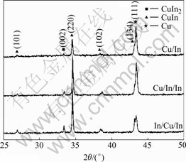
Fig.1 XRD spectra of three types of precursors
Fig.2 shows the SEM images of precursor derived from different deposition sequences. It can be seen that the surface of film with Cu/In sequence is uniform and dense, and the film well covers on the substrate (Fig.2(a)), while the surfaces of the films with Cu/In/In and In/Cu/In sequences become rougher and the lateral distances between individual droplets increase apparently (Figs.2(b) and 2(c)).
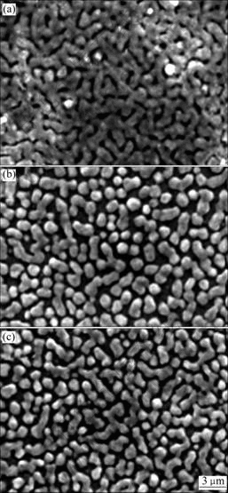
Fig.2 SEM images of Cu-In precursor deposited with different sequences: (a) Cu/In; (b) Cu/In/In; (c) In/Cu/In
Atomic force microscopy(ATM) was used to further characterize the structural properties of precursors. In Fig.3 the AFM three-dimensional images of three types of precursors are displayed, which represent the surface morphology as well as microstructure. The film with Cu/In sequence has a smooth surface with root-mean- square(RMS) roughness of approximate 77 nm. The RMS roughnesses of the films with Cu/In/In and In/Cu/In sequences are 87 and 88 nm, respectively. This is the result of grain competition. These observations are similar to those reported in Ref.[14]. This reveals that the surface roughness is related to the deposition sequence used. In addition, precursors deposited by different deposition sequence display granular surface structure, suggesting a three-dimensional island-like growth mechanism.
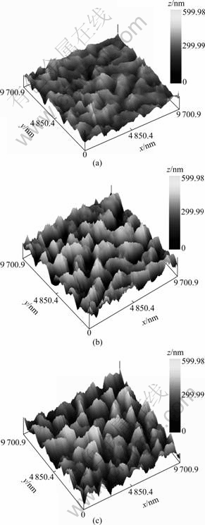
Fig.3 AFM images of Cu-In precursor deposited with different sequences: (a) Cu/In; (b) Cu/In/In; (c) In/Cu/In
3.2 Growth of CuInS2 films
In Fig.4, the XRD spectra of the sulfurized thin films for all the sequences are plotted. It can be seen from Fig.4(a) that the CuIn and CuIn2 phases are mainly discomposed to Cu11In9 phase after annealing treatment at 150 ℃. BOLCOVAGE et al[15] found that the phase Cu11In9 is stable at low temperatures rather than decomposition at 157 ℃. For the precursor of Cu/In deposition sequence, CuIn(220) phase still coexists in film apart from peaks of Cu11In9 phase. While for the precursors of Cu/In/In and In/Cu/In deposition sequences, only (111), (312), (112), and (313) diffraction peaks of Cu11In9 phase are detected. This can be due to the presence of alternative layers of Cu and In of precursor, which has improved the mixing and uniformity of the elements. This facilitates the energy transfer of the high mobility Cu atoms to the low-melting In atoms, causing the formation of Cu11In9 alloys.
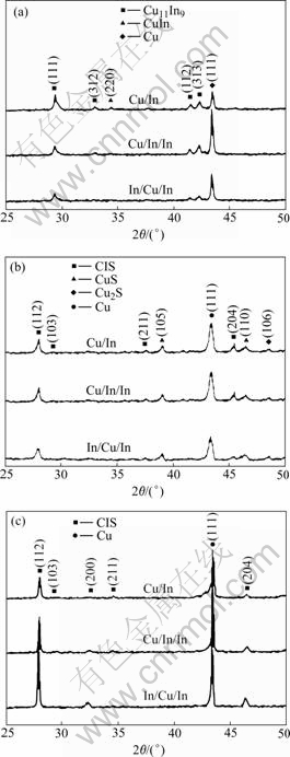
Fig.4 XRD spectra of sulfurized thin films at different temperatures: (a) 150 ℃; (b) 300℃; (c) 550 ℃
The XRD spectra corresponding to the 300 ℃- sulfurized films are plotted in Fig.4(b). For all films, CuInS2 chalcopyrite structure is confirmed by the presence of the characteristic peaks of chalcopyrite (103) [5]. The peaks at 27.3?, 29.2?, 37.5?, and 46.6?, corresponding to (112), (103), (211), and (204) reflections of the chalcopyrite, are clearly observed. In addition, diffraction peaks at 38.9?, 46.5? and 48.5? can be associated to binary compounds CuS(105), CuS(110), and Cu2S(106), respectively. This indicates that Cu2-xS (x=1, 2) is a preliminary by-product of CuInS2 formation. The Cu2-xS (x=1, 2) phase is mainly attributed to the high mobility of Cu and its migration towards the surface layers, which results in a non-uniform composition distribution and incomplete sulfurization reaction[16].
The XRD spectra corresponding to the 550 ℃- sulfurized films etched are plotted in Fig.4(c). It is obvious that the intensity and quantity of the chalcopyrite structure significantly increase, indicating the improvement of the crystalline quality of 550 ℃- sulfurized films etched. In case of random orientation, the intensity ratio of (112) to (204) peaks, should be 1.5[16]. The intensity ratio of I(112)/I(204), for these films, is very high, showing high degree of preferred orientation towards (112) reflection. It is worthy to note that the preferred orientation is the highest in the CIS films obtained from In/Cu/In precursor, indicating that the deposition sequence of In/Cu/In improves the crystalline quality of CIS films. The (112) preferred orientation in CIS films is beneficial for good lattice matching with CdS for efficient device fabrication[17].
The surface roughness and grain size of polycrystalline thin films were directly corrected to device efficiency. Surface roughness not only causes light scattering, but also increases the surface area and interface, which can lead to an increase in the carrier recombination rate[18]. The AFM images of the 550 ℃- sulfurized films etched, shown in Fig.5, provide direct visual information on both grain size and surface rough- ness. According to the AFM images, the average grain sizes range approximately from 500 nm to 1 200 nm. The surface roughnesses are 152, 95 and 70 nm corresponding to three types of sequences, as seen in a cross-sectional view of the surface corresponding to the line shown in Figs.5(a), (b) and (c). This indicates that the In/Cu/In sequence has smaller surface roughness and higher crystallinity. This result supports the XRD results in Fig.4(c).
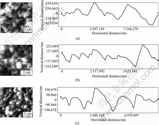
Fig.5 AFM images of CIS films with different precursors and corresponding cross-sectional views of surface: (a) Cu/In; (b) Cu/In/In; (c) In/Cu/In
3.3 Optical characteristics of CuInS2 films
We consider the optical properties of the CIS films mainly on band gap and absorption coefficient, which are essential for absorbing the solar radiation. To calculate the absorption coefficient  the following relation is used[14]:
where d is the film thickness, R and T are the reflection and transmission coefficient, respectively. All of these thin films have absorption coefficient of about 105 cm-1 above the fundamental band edge, which is very close to values reported[19]. It thus absorbs the incident light with photo energy higher than the band gap with a few microns.
The absorption coefficient α is related to the energy gap of Eg according to the equation:

where A is a constant, h is the Plank constant and n is equal to 1/2 for direct gap and 2 for an indirect gap. It is now well established that CuInS2 is a direct gap semiconductor with band extremely located at the centre of the Brillouin zone[20]. Based on the allowed direct interband transition, the band gap Eg is determined by extrapolating the straight line of the vs
vs  curve to intercept of the horizontal photon energy axis. As shown in Fig.6, the Eg for the 550 ℃-sulfurized films etched with different sequence can be estimated to be 1.3-1.4 eV, which is close to the value of 1.30 eV and 1.43 eV reported by other workers[14]. However, these values are smaller than the value of 1.53 eV for single crystal at room temperature[20], possibly due to the poor crystal quality and deviations from stoichiometry which gives rise to defect states and induces smearing of absorption edge. In addition, we observe that the Eg increases from 1.32 to 1.38 eV corresponding to the Cu/In and In/Cu/In sequences, and the optical absorption edge of In/Cu/In sequence is very steep, implying that the CIS films with In/Cu/In precursor have a good homogeneity in the shape and size of the grains.
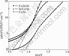
Fig.6 vs photon energy for CIS films with different precursors
4 Conclusions
1) The single-phase chalcopyrite CIS thin films with a strong (112) orientation is obtained by sulfurizing the films at 550 ℃ and etching in KCN solution at room temperature.
2) Although the final phase and crystallinity of CIS films are the same for three types of deposition sequences, the reaction ways are different. A higher reaction with sulfur is observed for the starting sequences with In.
3) The use of In/Cu/In precursor is found to improve not only the intensity of (112) preferred orientation but also the crystallographic, morphological, surface roughness, and optical properties. The improved CIS films are uniform, with single phase, showing an energy band gap of 1.38 eV and absorption coefficient of about 105 cm-1. This is due to the presence of alternative layers of Cu and In of precursor which has improved the mixing and uniformity of the elements.
4) The CuInS2 absorber layer prepared with In/Cu/In precursor provides a novel method to improve the performance of thin film solar cells.
References
[1] RAMAIAH K S, RAJA V S. AES and XPS analysis of CuIn(S1-xSex)2 thin films grown by spray pyrolysis technique [J]. Scripta Mater, 2001, 44: 771-777.
[2] BRAUNGER D, HARISKOS D, WALTER T, SCHOCK H W. An 11.4% efficient polycrystalline thin film solar cell based on CuInS2 with a Cd-free buffer layer [J]. Solar Energy Materials and Solar Cells, 1996, 40: 97-102.
[3] GOSSLAM, HAHN T H, METEZNER H, CONRAD J, GEYER U. Thin CuInS2 films by three-source molecular beam deposition [J]. Thin Solid Films, 1995, 268: 39-44.
[4] NAKAMURA S, YAMAMOTO A. Electrodeposited CuInS2-based thin-film solar cells [J]. Solar Energy Materials & Solar Cells, 2003, 75: 81-86.
[5] QIU Ji-jun, JIN Zheng-guo, QIAN Jin-wen, SHI Yong, WU Wei-bing. ILGAR CuInS2 films from various preparation conditions [J]. Materials Letters, 2005, 59: 2735-2740.
[6] YAMAGUCHI T, NAKA M, NIIYAMA S, IMANISHI T. Characterization of Cu(In,Ga)Se2 thin films prepared by evaporation from ternary compounds [J]. Journal of Physics and Chemistry of Solids, 2005, 66: 2000-2003.
[7] BANDYOPADHYAYA S, CHAUDHURI S, PAL A K. Synthesis of CuInS2 films by sulphurization of Cu/In stacked elemental layers [J]. Solar Energy Materials and Solar Cells, 2000, 60: 323-339.
[8] VON KLOPMANN C, DJORDJEVIC J, RUDIGIERE E, SCHEER R. Real-time studies of phase transformations in Cu-In-Se-S thin films (2): Sulfurization of Cu-In precursors [J]. Journal of Crystal Growth, 2006, 289: 121-133.
[9] KLENK R, BLIESKE U, DIETERLE V, ELLMER K, FIECHTER S, HENGEL I, J?GER-WALDAU A, KAMPSCHULTE T, KAUFMANN C H, KLAER J, LUX-STEINER M C H, BRAUNGER D, HARISKOS D, RUCKH M, SCHOCK H W. Properties of CuInS2 thin films grown by a two-step process without H2S [J]. Solar Energy Materials and Solar Cells, 1997, 49: 349-356.
[10] GUPTA A, ISOMURA S. Precursor modification for preparation of CIS films by selenization technique [J]. Solar Energy Materials and Cells, 1998, 53: 385-401.
[11] CABALLERO R, GUILL?N C. CuInSe2 formation by selenization of sequentially evaporated metallic layers [J]. Solar Energy Materials and Solar Cells, 2005, 86: 1-10.
[12] NAKANOT, SUZUKI T, OHNUKIN, BABA S. Alloying and electrical properties of evaporated Cu-In bilayer thin film [J]. Thin Solid Films, 1998, 334: 192-195.
[13] OGAWA Y, J?GER-WALDAU A, HUA T H, HASHIMOTO Y, ITO K. Influence of KCN treatment on CuInS2 thin films [J]. Applied Surface Science, 1996, 92: 232-236.
[14] GUEZMIR N, OUERFELLI J, BELGACEM S. Optical properties of sprayed CuInS2 thin layers [J]. Materials Chemistry and Physics, 2006, 96: 116-123.
[15] BOLCOVAGE A, CHEN S W, KAO C R, CHANG Y A, ROMING A D. Phase equilibria of Cu-In system (I): Experimental investigation [J]. Journal of Phase Equilibria, 1993, 14: 14-16.
[16] SHI Yong, JIN Zheng-guo, LI Chun-yan, AN He-song, QIU Ji-jun. Effect of [Cu]/[In] ratio on properties of CuInS2 thin films prepared by successive ionic layer absorption and reaction method [J]. Applied Surface Science, 2006, 252: 3737-3743.
[17] SHAO Le-xi, CHANG Kuen-huei, HWANG Huey-liang. Zinc sulfide thin films deposited by RF reactive sputtering for photovoltaic applications [J]. Applied Surface Science, 2003, 212/213: 305-310.
[18] RABEH M B, ZRIBI M, KANZARI M, REZIG B. Structural and optical characterization of Sn incorporation in CuInS2 thin films grown by vacuum evaporation method [J]. Materials Letters, 2005, 59: 3164-3168.
[19] MUDRYI A V, VICTOROV I A, GREMENOK V F, PATUK A I, SHAKIN I A, YAKUSHEV M V. Optical spectroscopy of chalcopyrite compounds CuInS2, CuInSe2 and their solid solutions [J]. Thin Solid Films, 2003, 431/432: 197-199.
[20] HENDERSON D O, MU R, UEDA A, WU M H, GORDON E M, TUNGY S, HUANG M, KEAY J, FELDMAN L C, HOLLINGSWORTH J A , BUHRO W E, HARRIS J D, HEPP A F, RAFFAELLR P. Optical and structural characterization of copper indium disulfide thin films [J]. Materials and Design, 2001, 22: 585-589.
Foundation item: Project(2006AA03Z2370) supported by the High-Tech Research and Development Program of China
Corresponding author: YAN You-hua; Tel: +86-10-58742809; E-mail: yanyouhua@atmcn.com
(Edited by YANG Bing)

