
Dielectrophoretic assembly of semiconducting single-walled carbon nanotube transistor
Se-Hun KWON1, Young-Keun JEONG1, Soongeun KWON2, Myung-Chang KANG1, Hyung-Woo LEE1
1. National Core Research Center for Hybrid Materials Solution, Pusan National University, Busan 609-735, Korea;
2. Department of Mechanical Engineering, Korea Advanced Institute of Science and Technology (KAIST),
Daejeon 305-701, Korea
Received 21 April 2010; accepted 10 September 2010
Abstract: A novel burning technique for making a semiconducting single-walled carbon nanotubes (SWNTs) transistor assembled by the dielectrophoretic force was suggested. The fabrication process consisted of two steps. First, to align and attach a bundle of SWNTs between the source and drain, the alternating (AC) voltage was applied to the electrodes. When a bundle of SWNTs was connected between two electrodes, some of metallic nanotubes and semi-conducing nanotubes existed together. The second step is to burn the metallic SWNTS by applying the voltage between two electrodes. With increasing the voltage, more current flowed through the metallic SWNTs, thus, the metallic SWNTs burnt earlier than the semiconducting one. This technique enables to obtain only semi-conducting SWNTs connection in the transistor. Through the I―V characteristic graph, the moment of metallic SWNTs burning and the characteristic of semi-conducing nanotubes were verified.
Key words: single-walled carbon nanotube (SWNT); semi-conducting carbon nanotube; burning technique; dielectrophoresis
1 Introduction
Carbon nanotube which has a rolled structure of a graphite sheet is made by chemical vapor deposition (CVD) or arc discharge method[1]. Single-walled carbon nanotubes (SWNTs) made by these methods have ~1.4 nm in diameter and, in the case of multi-walled carbon nanotubes (MWNTs), the diameter reaches 15-20 nm. Furthermore, carbon nanotubes (CNTs) have metallic or semi-conducting characteristics according to the structure of the chiral vectors[2]. Since 1991[3], CNTs have been used in many nanoscale applications due to their unique mechanical, electrical and chemical properties. Due to these specific characteristics, CNTs have been considered a prime candidate in numerous micro and/or nanoscale sensors and devices such as field emitted displays, fuel cells, electronic circuits and mechanical sensors[4-8].
Especially, since the most application needs to make a small size device, many researchers have studied how to move, align, and deposit carbon nanotubes on the special place. The most studies for the movement, alignment and deposition of carbon nanotubes have been done by chemical vapor deposition[1, 9]. Since this method has an advantage to grow carbon nanotubes simultaneously, it is so effective in mass producible assembly. However, this method needs very expensive facilities and it is so difficult to control CNTs’ length and to find the growth conditions. Since this process requires high temperature over 800 °C, furthermore, there is a compatibility problem in the fabrication process. Another method is to deposit carbon nanotubes manually. However, it is not easy to grip a carbon nanotube by the manipulator since carbon nanotubes are so tiny.
In this work, we tried to align and attach the CNTs at the room temperature by the dielectrophoretic force. By this method, we made semiconducting SWNTs transistor. When a bundle of SWNTs is connected between two electrodes, some of metallic SWNTs and semi-conducting SWNTs exist together. To retain only SWNTs, we proposed a new technique, the burning method. Through the analysis of the characteristics, we verified that only the semiconducting SWNTs were retained between two electrodes.
2 Fabrication process and background theory
2.1 Fabrication process
To align and attach a bundle of SWNTs, we fabricated a patterned device which was made by Ti and Au. Figure.1 shows the patterned electrodes which will work as a source and drain.
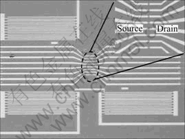
Fig.1 Optical microscope image of patterned device for semiconducting SWNTs transistor
The applied alternating (AC) voltage was 0.6 V/μm to 0.7 V/μm at 5 MHz, and the volume of the drops of the SWNTs solution was 0.5 μL to 1 μL. After dropping a droplet of SWNTs solution on the electric field applied electrodes, we could detect the deposition of CNTs between two electrodes by the oscilloscope.
To prepare the metal electrodes, we deposited Ti(200 ?)/Au(300 ?) on the patterned SiO2 (150 nm) by the photolithography process. To align and attach SWNTs, we applied AC voltage to the electrodes pair which can be used as source and drain. Palladium (Pd) as a secondary layer was deposited on the contact point of the nanotubes layer with 800 ?-thickness for making a ohmic contact. The width of main electrode was 10 μm and the gap between two electrode was 4-5 μm. We used SWNTs generally with 7-8 μm length and 2 nm diameter. To untangle and disperse the SWNTs, SWNTs solution was diluted and sonicated for several hours
2.2 Background theory for assembly
In this work, a driving force was used in the dielectrophoresis to assemble SWMTs, inducing that dipole moment, or polarization so particle can move, translate, and rotate along the gradient of electric field. When AC electric filed is applied to the electrodes, the polarization is induced on CNTs and a single CNT goes through a dipole moment due to non-uniform electric field. The dielectrophoretic force which arises due to the non-uniform electric fields can be expressed by the following equation[10].
 (1)
(1)
where a is the longest dimension of the particle; εm is the dielectric constant of medium; εp is the dielectric constant of the particle; and E is electric field. This force is affected by the applied frequency due to the complex permittivity expression,  , in which σ is conductivity and ω is the frequency of the AC electric field.
3 Simulation
In this work, the electrical characteristics between two electrodes were analyzed. To simulate a pre- experiment, we used a commercial program, FEMLAB?. Fig.2(a) shows a distribution of the electric field intensity when the current is applied between two sharp electrodes with 4 μm-gap distance. A simulation result of the round electrode is shown in Fig.2(b). As shown in Fig.2(a), in the case of the sharp electrodes, the electric intensity was concentrated on the center of the electrodes. The concentration of the electric intensity causes the attraction of CNTs to the center of the electrodes. However, it is not easy for CNTs to stay and attach at the center of the electrode since the electric field changes rapidly at the center of the electrode. In other words, the quasi-stable region is very narrow for CNTs to stay and attach on the desired place. In the case of a round electrode, the variation of the electric field is slow. So, it has a higher possibility for CNTs to stay on the center of the electrode.
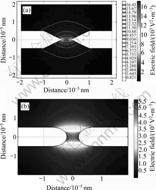
Fig.2 Distribution of electric field on sharp electrodes(a) and round electrodes(b)
4 Results and discussion
Fig.3(a) shows SEM image of a multi-electrode pattern used in this work. It is composed of 8 electrodes set by the sharp electrodes and the round ones by turns. The SWNTs powder used in this work is shown in Fig.3(a) as an inset. Fig.3(b) shows the result of a bundle SWNT deposition through the repeated experiments. From the scanning electron microscopy (SEM) images after each experiment, it was seen that a single bundle of SWNTs attached device was obtained by applying the frequency of 5 MHz and the intensity of 0.66 V/μm. The deposition yield of a single bundle of SWNTs was up to 70%.
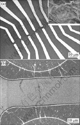
Fig.3 SEM images of 8 gaps array composed of round and sharp electrodes (SWNTs powder in a inset)(a) and a single bundle of SWNTs deposited electrodes(b)
When a bundle of SWNTs is attached between two electrodes, metallic nanotubes and the semi-conducting nanotubes exist together. To retain only semiconducting nanotubes, a novel technique called burning method is proposed. Since the metallic carbon nanotubes have the capability of higher current flow, most of the current goes through the metallic nanotubes when we apply direct current (DC) voltage to the main electrodes. With increasing the voltage step by step, the undesired metallic nanotubes burned one by one.
Finally, we obtained only semiconducting SWNTs deposited transistor. Fig.4(a) shows the I―V graph before burning the metallic carbon nanotubes, and Fig.4(b) shows the characteristics during the burning process. When the metallic SWNTs burn, as shown in Fig.4(b), the current drops suddenly. After burning the metallic SWNTs, we obtained only SWNTs deposited device which has the characteristic of the semi- conducting SWNTs, as shown in Fig.4(c).
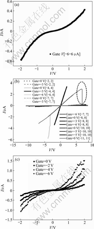
Fig.4 I―V characteristic graphs before burning process(a), during burning process(b) and after burning process(c)
5 Conclusions
1) A novel burning technique for making a semiconducting SWNTs transistor assembled by the dielectrophoretic force is suggested. Through the experiments, we deposited a single bundle of SWNTs between two electrodes by applying the frequency of 5 MHz and the intensity of 0.66 V/μm. Under this condition, the deposition yield of a single bundle of SWNTs is up to 70%. When a bundle of SWNTs is attached between two electrodes, metallic nanotubes and the semi-conducting nanotubes exist together.
2) To retain only semiconducting nanotubes, a novel technique called burning method is proposed. Through burning the metallic carbon nanotubes, we obtained only semiconducting attached SWNTs transistor.
Acknowledgements
The first and the second authors contributed equally to this work.
References
[1] DAI H. Nanotube growth and characterization [J]. Topics Applied Physics, 2001, 80: 29-53.
[2] MCEUEN P L. Single-walled carbon nanotubes electronics [J]. IEEE Transaction on Nanotechnology, 2001, 1: 78-85.
[3] IIJIMA S. Helical microtubules of graphitic carbon [J]. Nature, 1991, 354: 56-58.
[4] MARTEL R, SCHMIDT T, SHEA H R, HERTEL T, AVOURIS P. Single- and multi-wall carbon nanotube field effect transistors [J]. Applied Physics Letters, 1998, 73: 2447-2449.
[5] BACHTOLD A, HADLEY P, NAKANISHI T, DEKKER C. Logic circuits with carbon nanotube transistors [J]. Science, 2001, 294: 1317-1320.
[6] KONG J, FRANKLIN N R, ZHOU C, CHAPLINE M G, PENG S, CHO K, DAI H. Nanotube molecular wired as chemical sensors [J]. Science, 2000, 287: 622-625.
[7] RUECKES T, KIM K, JOSELEVICH E, TSENG G Y, CHEUNG C, LIEBER C M. Carbon nanotube-based nonvolatile random access memory for molecular computing [J]. Science, 2000, 289: 94-97.
[8] BIERCUK M J, MASON M, MARCUS C M. Local gating of carbon nanotubes [J]. Nano Letters, 2004, 4: 1-4.
[9] FRANKLINE N R. Patterned growth of single-walled carbon nanotubes on full 4-inch wafers [J]. Applied Physics Letters, 2001, 79: 4571-4573.
[10] POHL H A. Dielectrophoresis: The behavior of neutral matter in nonuniform electric field [M]. Cambridge: Cambridge University Press, 1978.
(Edited by YANG Hua)
Foundation item: Project (2010-0008-276) supported for two years by Pusan National University Research Grant, by NCRC(National Core Research Center) through the National Research Foundation of Korea funded by the Ministry of Education, Science and Technology, and by Pusan National University Research Grant, 2009.
Corresponding author: Hyung-Woo LEE; Tel: +82-51-5103160; E-mail: LHW2010@pusan.ac.kr; Myung Chang KANG, E-mail: kangmc@pusan.ac.kr

