Trans. Nonferrous Met. Soc. China 23(2013) 1390-1394
Fabrication of titanium oxide films at low temperature from aqueous solution
Wen-ning MU1, Yu-chun ZHAI2, Shuang-zhi SHI3
1. School of Resources and Materials, Northeastern University at Qinhuangdao Branch, Qinhuangdao 066004, China;
2. Department of Metallurgical Physical Chemistry, Northeastern University, Shenyang 110819, China;
3. Qinhuangdao Shougang Plate Co., Ltd, Qinhuangdao 066003, China
Received 27 April 2012; accepted 28 July 2012
Abstract: Titanium oxide thin films were prepared on self-assembled monolayers-coated silicon substrate using layer-by-layer self-assembly method and chemical bath deposition from an aqueous solution. The effects of temperature on structural properties, thickness and morphologies of titanium oxide thin films were investigated. The results show that the absorption peak of peroxo complexes of titanium at 410 nm decreases gradually with increasing the temperature. The deposited films consisting of titanium oxide nanocrystals are believed to be fully amorphous by XRD. Titanium oxide thin films fabricated at 60 °C for 2 h are continuous, dense and homogeneous with a size in the range of 20-40 nm by SEM. The chemical compositions of deposited thin films were studied by EDS, and the mole ratio of O to Ti is 2.2:1.
Key words: titanium oxide; thin film; chemical bath deposition; self-assembly method
1 Introduction
Thin films of titanium oxide are widely used in microelectronics [1], optical cells [2], solar energy conversion [3], high-efficiency catalysts [4], microorganism photolysis [5] and self-cleaning coatings [6], due to their high transparency, excellent mechanical durability [7] and charge transport properties. Accordingly, the fabrication of titanium oxide thin films has been attempted by several techniques in the past decades such as sol-gel process [8], chemical vapor deposition (CVD) [9], various reactive sputtering methods [10], evaporation [11], ion beam assisted processes [12], atomic layer deposition [13,14] and filtered arc deposition [15]. However, the application of these processes is limited because of the high temperature, high qualitative vacuum system and high cost.
At present, a relatively new technique of layer-by-layer self-assembly (LbL) was widely used for the fabrication of organic films because of its simple process, low temperature deposition, no limit of thickness and no need of complicated equipments [16]. The method consists of alternate absorption of positively and negatively charged polymers (polycations and polyanions) from their respective solutions, and is driven by general electrostatic attraction. Repeating each immersion step leads to surface charge reversal while multiple immersion results in the formation of organic self-assembled multilayer on the substrate. The nanostructure of films is readily changed by adjusting the pH of solution. Moreover, there has been a growing interest in low-temperature thin film deposition techniques from aqueous solutions in recent years. One typical example is chemical bath deposition (CBD) method which operates at low temperatures (30-100 °C) in aqueous environments [17]. The method offers a lower capital equipment cost, lower processing temperature, and greater flexibility in the choice of substrates. Metal oxides could be formed on the self-assembled monolayers (SAMs) in aqueous solutions by simulating the bio-inspired processing [18].
This work aims to prepare titanium oxide thin films on SAMs-coated single crystal silicon substrate from titanate aqueous solution by layer-by-layer self-assembly method and chemical bath deposition. The effects of temperature on thickness and morphology of titanium oxide thin films were discussed. The chemical feature, phase composition and morphology of the thin films were analyzed by energy dispersive spectrometer (EDS), X-ray diffraction analysis (XRD) and scanning electron microscope (SEM), respectively.
2 Experimental
2.1 Chemicals and substrates
Sodium poly(styrenesulfonate) (PSS, Mr=70000), poly(allyllamine-hydrochloride) (PAH, Mr=60000) and polyethyleneimine (PEI, Mr=70000) were purchased from Aldrich. TiCl4 (Sinopharm Chemical Reagent Co. Ltd., China), H2O2 (Sinopharm Chemical Reagent Co. Ltd., China), HCl and H2SO4 (Beijing Chemical Reagent Factory, China) were used without further purification. The p-type Si (100) wafers (Hefei Kejing Materials Technology Co. Ltd., China) were used as the substrates. All other chemicals were of reagent grade, and water was purified twice by ion exchange and subsequent distillation.
2.2 Deposition of SAMs
The single crystal silicon wafers were first ultrasonically cleaned in sequence of chloroform, acetone and ethanol, so that organic impurities on the surface of substrates could be removed. The wafers were then immersed in a piranha solution (3:1 concentrated H2SO4/H2O2) at 80 °C for 40 min. The silicon surface was activated to form a negatively charged hydrophilic SiOH layer, which is necessary for the following SAMs preparation [19]. After being cleaned, the silicon wafers were rinsed with deionized water and dried completely in nitrogen.
The SAMs of the silicon wafers (after Piranha treatment) were fabricated by the alternated immersion for 20 min into PEI solutions (1.25 g/L, pH=9.0) and then into PSS solutions (4 g/L, containing 0.5 mol/L MnCl2 at pH 3.5), followed by immersion into PAH solutions (2 g/L, containing 0.5 mol/L NaCl at pH 3.5). Samples were thoroughly rinsed between immersions in ultra-pure water to weakly remove bound molecules. After the second layer, only PAH and PSS were used, and this sequence was repeated four times. The films consisting of one-layer PEI/PSS couples and four-layer PAH/PSS couples were known as SAMs. SAMs-coated substrates were then ultrasonically cleaned with deionized water and dried completely with nitrogen gas.
2.3 Fabrication of titanium oxide thin films
A fresh titanium precursor solution was prepared by dissolving TiCl4 into 30% H2O2 solution. The concentration of titanium was adjusted to 10 mmol/L by diluting with deionized water. The SAMs-coated substrates were put into a silicon tube containing precursor solution and hydrochloric acid with the mole ratio of 1:1. The silicon tube was then kept in water bath at varied temperatures for 2 h. The peristaltic pump was used as a driving device for the circulation of reaction solution during the fabrication process of titanium oxide thin films, and the flow rate of reaction solution was maintained at 20 mL/min. After a desired deposition time was reached, the substrates were taken out, ultrasonically washed with deionized water, and dried with nitrogen gas.
2.4 Characterization methods
The phase structure of thin films was determined by an X-ray diffractometer (XRD) operating with a Cu Ka radiation at a scanning speed of 1.2 (°)/min. The morphologies of thin films were investigated with an SSX-550 scanning electron microscope, and the chemical composition on the surface of these films was gained by an energy dispersive spectrometer (EDS). In order to know the information on thickness of thin films, a surface profile measuring system (Sloan, Dektak3030) was employed. The a UV-vis spectrum of solution was determined using UV-visible absorption spectrometer (Shimadzu, UV-3100). The functional groups of the SAMs were analyzed by 8400S CE Fourier transformation infrared spectrometer.
3 Results and discussion
3.1 SAMs formation
The transmission infrared spectrum of the film coated on silicon substrate in the frequency range of 3100-2700 cm-1 is shown in Fig. 1. It can be seen that the peak frequencies for asymmetric and symmetric methylene vibrations, vs (CH2) and vas (CH2), are located at 2852 and 2923 cm-1, respectively. However, the peak frequencies of ―SO3H are not observed due to the weak signals.
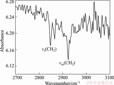
Fig. 1 Transmission IR spectrum of film on silicon substrate in high-frequency region
In Fig. 2, representative SEM image of thin film after the modification of polyelectrolytes is presented. It is evident that the deposited layer is continuous, uniform and dense, and the thickness of thin film detected by a surface profile measuring system is about 10 nm. Energy dispersive spectrometry (EDS) analysis (inset in Fig. 2) indicates that the thin film prepared contains C, N, O and S elements. These elements are necessary for the formation of SAMs.

Fig. 2 Morphology and EDS spectrum of thin film
3.2 Solution chemistry of titanium precursor
The aqueous solutions presented a change in appearance during the fabrication of titanium oxide thin films. The color of the fresh titanium precursor solution was originally orange-red. The UV-vis spectra of the solutions are shown in Fig. 3. The strong absorption peak at a wavelength of 410 nm indicates the presence of peroxo complexes of titanium. Upon heating, the solutions showed rapid discoloration in some cases with the occurrence of turbidity.
The higher the heating temperature was, the faster the solution was discolored while keeping the other experimental conditions invariable until it is nearly colorless. From Fig. 3, it can be seen that the deposition temperature has a noticeable influence on the transmittance of peroxo complexes of titanium, the absorption peak at 410 nm decreases gradually with increasing the temperature. The concentration of peroxo complexes of titanium is high owing to the metastable characteristic of titanium precursor solution at room temperature. However, it will decrease with the increase of temperature. When the temperature reaches 60 °C, the absorption peak at a wavelength of 410 nm nearly disappears, which illustrates that the peroxo complexes of titanium in aqueous solution approximately react completely. The chemical reactions involved in the aqueous solution can be outlined as follows:
 =
= (1)
(1)
 =
= (2)
(2)
Based on these chemical reactions, titanium oxide films were fabricated on silicon substrates modified with SAMs. The phase structure of titanium oxide films is presented in Fig. 4, in which it can be observed that the structure of the thin films exhibits only short-range order, and it is an amorphous titanium oxide layer.
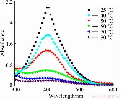
Fig. 3 UV-vis spectra of solution at different temperatures

Fig. 4 XRD pattern of titanium oxide thin films
3.3 Characterization of titanium oxide thin films
The morphologies of titanium oxide films prepared at different temperatures are shown in Fig. 5. As can be seen, the deposited layers are continuous and uniform with a size in the range of 20-40 nm on the film surface when the temperature is 60 °C (Fig. 5(a)). After being heated to 70 °C, parts of the particles begin to grow up and the spaces between particles are filled with some small particles, thereby inevitably leading to the formation of unsmooth and inhomogeneous surface eventually seen in Fig. 5 (b). The particle size of the thin films varies in the range of 40-160 nm. When the temperature rises to 80 °C, it is obviously observed from Fig. 5 (c) that the thin films are no longer continuous and dense, and the particles on the surface grow along vertical direction. In contrast, the particle size increases and mainly concentrates in the range of 250-350 nm.

Fig. 5 SEM images of titanium oxide thin film at temperatures of 60 °C (a), 70 °C (b) and 80 °C (c)
The results of film thickness detected by a surface profile measuring system in Fig. 6 show that the thin film grows with an increase in reaction temperature. At 60 °C, the thickness is 54 nm; it increases to 95 nm at 80 °C.
The thin film obtained at 60 °C was analyzed by the energy dispersive spectrometer (EDS), and the results are shown in Fig. 7. It is evident that the major compositions of deposited thin films are titanium and oxygen, and the mole ratio of O to Ti is 2.2:1, as presented in Fig. 8, which is somewhat higher than the corresponding ratio of 2:1 of stoichiometric TiO2 because the grown films contain some amount of water [20].

Fig. 6 Thickness of thin film prepared at different temperatures

Fig. 7 EDS spectrum of thin film

Fig. 8 Content distribution of chemical elements on thin film surface
4 Conclusions
Titanium oxide films grew on SAMs-coated single crystal silicon substrates using layer-by-layer self- assembly method and chemical bath deposition via a hydrolysis of TiCl4 in an acid environment. The results of UV-vis spectra show that the temperature has a noticeable influence on the transmittance of peroxo complexes of titanium and the absorption peak at 410 nm decreases gradually with increasing the temperature. The thickness of titanium oxide thin films varies between 54 and 95 nm with increasing the temperature from 60 °C to 80 °C. The deposited layers consisting of titanium oxide nanocrystals are believed to be fully amorphous by XRD. The morphologies of titanium oxide films prepared at 60 °C for 2 h are continuous, dense and homogeneous, and the size of deposition particles varies from 20 nm to 40 nm. The major chemical compositions of thin films are Ti and O, and the mole ratio of O to Ti is 2.2:1.
References
[1] BURN G P. Titanium dioxide dielectric films formed by rapid thermal oxidation [J]. Journal of Applied Physics, 1989, 65(5): 2095-2097.
[2] YOLDAS B E, O’KEEFFET W. Antireflective coatings applied from metal-organic derived liquid precursors [J]. Applied Optics, 1979, 18(18): 3133-3138.
[3] BUTLER M A, GINLEY D S. Principles of photoelectrochemical, solar energy conversion [J]. Journal of Materials Science, 1980, 15(1): 1-19.
[4] CARLSON T, GIFFIN G L. Photooxidation of methanol using vanadium pentoxide/titanium dioxide and molybdenum trioxide/titanium dioxide surface oxide monolayer catalysts [J]. The Journal of Physical Chemistry, 1986, 90: 5896-5900.
[5] MATSUNAGA T, TOMODA R, NAKAJIMA T, KOMINE T. Reductive dechlorination of hexachlorobenzene to tri- and dichlorobenzenes in anaerobic sewage sludge [J]. Applied and Environmental Microbiology, 1988, 54: 327-330.
[6] WANG R, HASHIMOTO K, FUJISHIMA A, CHIKUNI M, KOJIMA E, KITAMURA A, SHIMOHIGOSHI M, WATANABE T. Light-induced amphiphilic surfaces [J]. Nature, 1997, 388(6641): 431-432.
[7] OKADA Y, YAMADA Y, JIN P, TAZAWA M, YOSHIMURA K. Fabrication of multifunctional coating which combines low-property and visible-light-responsive photocatalytic activity [J]. Thin Solid Films, 2003, 442(1-2): 217-221.
[8] MALLAK M, BOCKMEYER M,  P. Liquid phase deposition of TiO2 on glass: Systematic comparison to films prepared by sol-gel processing [J]. Thin Solid Films, 2007, 515(20-21): 8072-8077.
[9] MILLS A, ELLIOTT N, PARKIN I P, O’NEILL S A, CLARK R J. Novel TiO2 CVD films for semiconductor photocatalysis [J]. Journal of Photochemistry and Photobiology A, 2002, 151(1-3): 171-191.
[10] MIAO L, JIN P, KANEKO K, TERAI A, GABAIN N N, TANEMURA S. Preparation and characterization of polycrystalline anatase and rutile TiO2 thin films by rf magnetron sputtering [J]. Applied Surface Science, 2003, 212-213: 255-263.
[11] FUJII T, SAKATA N, TAKADA J, MIURA Y, DAITOH Y, TAKANO M. Characteristics of titanium oxide films deposited by an activated reactive evaporation method [J]. Journal of Materials Research, 1994, 9(6): 1468-1473.
[12] LIN S S, HUNG Y H, CHEN S C. Optical properties of TiO2 thin films deposited on polycarbonate by ion beam assisted evaporation [J]. Thin Solid Films, 2009, 517(16): 4621-4625.
[13] AARIK J, AIDLA A, KIISLER A A, UUSTARE T, SAMMELSELG V. Effect of crystal structure on optical properties of TiO2 films grown by atomic layer deposition [J]. Thin Solid Films, 1997, 305(1-2): 270-273.
[14] SUISALU A, AARIK J,  H, SILDOS I. Spectroscopic study of nanocrystalline TiO2 thin films grown by atomic layer deposition [J]. Thin Solid Films, 1998, 336(1-2): 295-298.
[15] BENDAVID A, MARTOIN P J, TAKIKAWA H. Deposition and modification of titanium dioxide thin films by filtered arc deposition [J]. Thin Solid Films, 2000, 360(1-2): 241-249.
[16] MA J, JIA Y, JING Y, YAO Y, J. SUN J. Synthesis and photocatalytic activity of TiO2-hectorite layer-by-layer thin films [J]. Applied Clay Science, 2010, 47: 433-437.
[17] de GUIRE M R, NIESEN T P, SUPOTHINA, WOLF J, BILL J, DUBENIK C N, ALDINGER F, HEUER A H,  M. Synthesis of oxide and non-oxide inorganic materials at organic surfaces [J]. Z Metallk D, 1998, 89: 758-766.
[18] GAO Y F, KOUMOTO K. Bio-inspired ceramic thin film processing: Present status and future perspectives [J]. Crystal Growth & Design, 2005, 5(5): 1983-2017.
[19] SEU K J, PANDEY A P, HAQUE F, PROCTOR E A, RIBBE A E, HOVIS J S. Effect of surface treatment on diffusion and domain formation in supported lipid bilayers [J]. Biophysical Journal, 2007, 92: 2445-2450.
[20] FUCHS T M, HOFFMANN R C, NIESEN T P, BILL J, ALDINGER F. Deposition of titania thin films from aqueous solution by a continuous flow technique [J]. Journal of Materials Chemistry, 2002, 12: 1597-1601.
低温条件下在水溶液中制备二氧化钛薄膜
牟文宁1,翟玉春2,石双志3
1. 东北大学(秦皇岛分校) 资源与材料学院,秦皇岛 066004;
2. 东北大学 冶金物理化学研究所,沈阳 110819;
3. 秦皇岛首钢板材有限公司,秦皇岛 066003
摘 要:利用化学浴沉积和层-层自组装方法,在含有自组装涂层硅衬底上制备二氧化钛薄膜。研究温度对二氧化钛薄膜结构、厚度和微观形貌的影响。紫外可见光谱结果表明,钛过氧配合物在410 nm处的吸收峰强度随着温度的升高而逐渐减小。由XRD分析结果可知,沉积的纳米二氧化钛薄膜为无定形层。SEM分析结果表明,在温度60 °C、时间2 h时可制得连续、致密、均一的二氧化钛薄膜,粒度分布为20~40 nm间。EDS分析表明薄膜的化学组成为O和Ti,两者的摩尔比为2.2:1。
关键词:二氧化钛;薄膜;化学浴沉积;自组装方法
(Edited by Xiang-qun LI)
Foundation item: Projects (51204036, 51234009) supported by the National Natural Science Foundation of China; Project (20110042120014) supported by the Research Fund for the Doctoral Program of Higher Education, China
Corresponding author: Wen-ning MU; Tel: +86-335-8071038; E-mail: danae2007@163.com
DOI: 10.1016/S1003-6326(13)62608-4

