
Effect of process parameters on electrical, optical properties of IZO films produced by inclination opposite target type DC magnetron sputtering
Do-Hoon SHIN1, Yun-Hae KIM2, Joong-Won HAN2, Kyung-Man MOON2, Ri-Ichi MURAKAMI3
1. Korean Air Aerospace Division, Korean Air Lines Co., 103 Daejeo 2-dong, Gangseo-gu, Busan, 618-142, Korea;
2. Department of Mechanical and Material Engineering, Korea Maritime University, Dongsam-dong,
Youngdo-ku, Busan, Korea;
3. Department of Mechanical Engineering, The University of Tokushima, 2-1 Minami-josanjima-cho,
Tokushima, 770-8506, Japan
Received 18 June 2008; accepted 10 March 2009
Abstract: IZO films were deposited onto PET substrate at room temperature with the inclined opposite target type DC magnetron sputtering equipment, in which a sintered oxide IZO target (doped with 10% ZnO, packing density of 99.99%) was used. The effects of total sputtering pressure and film thickness on IZO films properties were studied. All the films produced at room temperature have a amorphous structure, irrespective of the total sputtering pressure and film thickness. A resistivity of the order of 10-4 Ω?cm was obtained for IZO films deposited at lower pressure (film thickness of 190 nm). The resistivity of IZO films deposited at room temperature depends on film thickness and shows a minimum at a thickness of 530 nm.
Key words: indium-zinc-oxide(IZO); inclination opposite target type DC magnetron sputtering; transparent conductive oxide(TCO); electromagnetic wave shielding effectiveness(SE)
1 Introduction
Transparent conductive oxide(TCO) films have been widely used in a variety of applications such as transparent conducting electrodes in touch panels, flat panel displays and electromagnetic interference(EMI) shielding of plasma display panel(PDP)[1-2]. Indium-tin oxide(ITO) films are the most extensively studied and commonly used as ones of TCO films. ITO films having a high electric conductivity and high transparency are easily fabricated on glass substrates at a substrate temperature over 473 K[3]. However, glass substrates are somewhat heavy and brittle, whereas polymeric substrates (such as polycarbonate, acrylic and polyethylene terephthalate) are lightweight, unbreakable, conveniently portable, and so on[4-5]. For these reasons, it has been recently suggested to use polymeric materials as substrates for transparent conductive applications instead of glass. Many researchers have tried to produce high quality thin films at low temperatures by using several methods[4, 6-7]. However, amorphous ITO films exhibit a decrease in electrical conductivity and optical transparency with time and a very poor chemical stability [8]. These problems could be solved by using indium- zinc-oxide(IZO) films which have been deposited using variety of techniques and were recently reported to exhibit excellent chemical stability with highly electrical conductivity and optical transparency[8-10]. In the present work, IZO films were produced on PET substrates using an In2O3-ZnO (In2O3 90% and ZnO 10%, mass fraction) at room temperature using inclination opposite target type DC magnetron sputtering technology.
2 Experimental
IZO films were fabricated on PET substrates (50 mm×150 mm×0.05 mm) by inclination opposite target type DC magnetron sputtering, as shown in Fig.1, using a sintered oxide IZO target (doped with 10% in mass fraction ZnO, packing density of 99.99%) without heating. The PET substrate was ultrasonically cleaned for 5 min using methanol as a solvent. The evaporation chamber was evacuated down to 4×10⁻³ Pa prior to deposition. Argon gas (99.999% purity) was then introduced into the chamber. The constitution of IZO films was determined by X-ray diffractometer(XRD) with 45 kV, 40 mA Cu Kα radiation using RINT 2000 (Rigaku). XRD analysis confirmed that all the films were amorphous, irrespective of the total sputtering pressure and film thickness. The film thickness was measured using a Dektak3 surface profiler (VEECO/Sloan Tech.). Resistivity, carrier concentration and Hall mobility were determined using van der Pauw method at room temperature with a magnetic field strength of 0.37 T. Optical transmittance was measured in the wavelength range of 200-2 500 nm using a spectrophotometer (JASCO, V-550) without a bare substrate in the path of the reference beam. The surface morphology of films was observed using field emission scanning electron microscope (FESEM, S-4700, Hitachi) and atomic force microscope (AFM, spa300, SII).
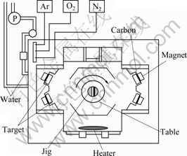
Fig.1 Schematic diagram of inclination opposite target type DC magnetron sputtering equipment
3 Results and discussion
Figs.2(a) and (b) show the change of the deposition rate, resistivity, carrier density and Hall mobility of the films as a function of the total sputtering pressure(ps) for the IZO films deposited on PET substrates. The film thickness of all these samples is 190 nm. The variation in deposition rate with ps can be seen in Fig.2(a), which shows that it increases slightly with increasing ps from 0.32 to 0.83 Pa.

Fig.2 Variation of resistivity and deposition rate (a), carrier density and Hall mobility (b) as function of total sputtering pressure
The resistivity of the films is not affected by the increase in total sputtering pressure from 0.32 to 0.55 Pa (Fig.2(a)), but it increases very sharply for pressures above 0.55 Pa. The carrier density (Fig.2(b)) reaches a maximum value of 5.99×1020 cm-3 at 0.55 Pa and decreases to 1.23×1020 cm-3 when pressure is increased to 0.83 Pa. This decrease in carrier density may be related to a decrease of the number of oxygen vacancies
in the films. The Hall mobility decreases monotonically with increasing ps from 0.32 to 0.83 Pa. This decrease in the Hall mobility with increasing ps may result from the combined effects of increasing ionized scattering centers (0.32-0.55 Pa) and neutral scattering centers (above 0.55 Pa)[9].
An important result from this study is that a low resistivity of the order of 10-4 Ω?cm has been obtained for IZO films deposited at the lower end of the pressure range. It has been also reported by MENG and DOS SANTOS[10] that ITO films deposited at low pressure have a high Hall mobility, which leads to a decrease in the resistivity.
Figs.3(a) and (b) show the transmittance in the UV- visible and near infrared region for IZO films deposited at various ps.

Fig.3 Variation of transmittance as function of total sputtering pressure(ps)
For comparison, transmittance of a bare substrate (PET) is also shown in Fig.3. In the visible range, the absolute transmittance is 90%-93%, regardless of total sputtering pressure. On the other hand, a notable change in transmittance in the near infrared region with total sputtering pressure is observed. This behavior can be explained by Drude’s theory. In this region, the variation in transmittance is related to reflectivity corresponding to the plasma frequency ωp of the free carriers[9]:
 (1)
(1)
where n is the carrier density, e the elementary charge, ε0 the electronic constant of free space, εopt the optical relative permittivity, and m* the electron effective mass.
The value of λp calculated using Eq.(1) shows a decrease from 3 295 to 1 493 nm with the change of the carrier density. Thus, the variation in transmittance with ps can be attributed to the change in the carrier density. In the UV region, as shown in Fig.3(b), the wavelength at which transmittance reaches 30% decreases with the increase in the carrier density. This decrease in transmittance may be due to the shift of the band-gap [11].
Figs.4(a) and (b) show the variation of resistivity, carrier density and Hall mobility of the films as a function of film thickness for IZO films deposited on PET substrates. For all these samples, the total sputtering pressure was 0.32 Pa.

Fig.4 Resistivity (a), carrier density and hall mobility (b) of IZO films for various film thicknesses
Resistivity decreases when film thickness increases from 130 to 530 nm (Fig.4(a)). Despite some scattering in the data, as shown in Fig.4(b), carrier density increases with increasing thickness, which could be the origin of the decrease of resistivity since Hall mobility is almost independent of thickness.
Figs.5(a) and (b) show AFM (1 μm×1 μm) and SEM images of IZO films with a film thickness of 130 nm, 190 nm and 530 nm, respectively.

Fig.5 AFM (a1, a2, b3) and SEM (b1, b2, b3) images of IZO films with various thickness deposited at total sputtering pressure of 0.32 Pa: (a1) and (b1) 130 nm (Ra=1.23 nm); (a2) and (b2) 190 nm (Ra=1.55 nm); (a3) and (b3) 530 nm (Ra=3.0 nm)
As film thickness increases from 130 to 190 and 530 nm, surface roughness increases from 1.23 to 1.55 and 3.0 nm, which results from an increase of grain size from ~28 to ~40 nm.
A similar tendency has been reported by QIAO et al [12]. It has also been reported by KIM et al[13] that the larger grain size results in a lower density of grain boundaries which behave as traps for free carrier. Thus, the increase of carrier density with increasing film thickness is due to a decrease of grain boundary scattering, which results from the increased grain size. Consequently, as shown in Figs.4(a) and (b), an increase of carrier density leads to the decrease of the resistivity.
4 Conclusions
1) The films prepared at low pressure have low electrical resistivity of the order of 10-4 Ω・cm.
2) The change in carrier density with the total sputtering pressure produces a variation in transmittance in the UV and near infrared regions. In the visible range, the absolute transmittance is 90%-93%, regardless of the total sputtering pressure.
3) Resistivity decreases with increasing film thickness, which can be explained by an increase of carrier density with decreasing grain boundary scattering.
Acknowledgement
This research is financially supported by the Ministry of Education, Science Technology (MEST) and Korea Industrial Technology Foundation (KOTEF) through the Human Resource Training Project for Regional Innovation.
References
[1] KIM V M, KU D Y, LEE I K, SEO Y W, CHEONG B K, LEE T S, KIM I J, LEE K S. The electromagnetic interference shielding effect of indium-zinc oxide/silver alloy multilayered thin films [J]. Thin Solid Films, 2004, 473: 315-320.
[2] MINAMI T, KAKUMA T, TAKATA S. Preparation of transparent and conductive In2O3-ZnO films by radio frequency magnetron sputtering [J]. J Vac Sci Technol, 1996, A14: 1704-1708.
[3] WU W F, CHIOU B S. Properties of radio-frequency magnetron sputtered ITO films without in-situ substrate heating and post-deposition annealing [J]. Thin Solid Films, 1994, 247: 201-207.
[4] KIM H, HORWITZ J S, KUSHTO G P, KAFAFI Z H, CHRISEY D B. Indium tin oxide thin films grown on flexible plastic substrates by pulsed-laser deposition for organic light-emitting diodes [J]. Applied Physics Letters, 2001, 79: 284-290.
[5] FAHLAND M, KARLSSON P, CHARTON C. Low resisitivity transparent electrodes for displays on polymer substrates [J]. Thin Solid Films, 2001, 392: 334-337.
[6] SHIN J H, SHIN S H, PARK J I. Properties of DC magnetron sputtered indium tin oxide films on polymeric substrates at room temperature [J]. J Appl Phys, 2001, 89: 5199-5203.
[7] de CARVALHO C N, LAVAREDA G, FORTUNATO E, AMARAL A. Properties of ITO films deposited by r.f.-PERTE on unheated polymer substrates―Dependence on oxygen partial pressure [J]. Thin Solid Films, 2003, 427: 215-218.
[8] KIM H M, JUNG S K, AHN J S, KANG Y J, JE K C. Electrical and optical properties of In2O3-ZnO films deposited on polyethylene terephthalate substrates by radio frequency magnetron sputtering [J]. Jpn J Appl Phys, 2003, 42: 223-227.
[9] SONG P K, SHIGESATO Y, KAMEI M, YASUI I. Electrical and structural properties of tin-doped indium oxide films deposited by dc sputtering at room temperature [J]. Jpn J Appl Phys, 1999, 38: 2921-2927.
[10] MENG L J, DOS SANTOS M P. Properties of indium tin oxide (ITO) films prepared by r.f. reactive magnetron sputtering at different pressures [J]. Thin Solid Films, 1997, 303: 151-155.
[11] HAMBERG I, GRANQVIST C G. Evaporated Sn-doped In2O3 films: Basic optical properties and applications to energy-efficient windows [J]. J Appl Phys, 1986, 60: R123-R160.
[12] QIAO Z, LATZ R, MERGEL D. Thickness dependence of In2O3:Sn film growth [J]. Thin Solid Films, 2004, 466: 250-258.
[13] KIM H, HORWITZ J S, KUSHTO G, PIQUE A, KAFAFI Z H, GILMORE C M. Effect of film thickness on the properties of indium tin oxide thin films [J]. J Appl Phys, 2000, 88: 6021-6025.
Corresponding author: Yun-Hae KIM; Tel: +82-51-410-4966; E-mail: yunheak@hhu.ac.kr
DOI: 10.1016/S1003-6326(08)60394-5
(Edited by YANG Bing)

