
Ellipsometric analysis and optical absorption characterization of nano-crystalline diamond film
WANG Lin-jun(王林军)1, JIANG Li-wen(蒋丽雯) 1, REN Ling(任 玲) 1, LIU Jian-min(刘健敏) 1, SU Qing-feng(苏青峰) 1, XU Run(徐 闰) 1, PENG Hong-yan(彭鸿雁) 1, 2, SHI Wei-min(史伟民) 1, XIA Yi-ben(夏义本) 1
1.School of Materials Science and Engineering, Shanghai University, Shanghai 200072, China;
2.Physics Department, Mudanjiang Normal College, Mudanjiang 157012, China
Received 10 April 2006; accepted 25 April 2006
Abstract: A nano-crystalline diamond (NCD) film with a smooth surface was successfully deposited on silicon by a hot filament chemical vapor deposition (HFCVD) method. Scanning electron microscopy (SEM), atomic force microscopy (AFM), RAMAN scattering spectra, as well as spectroscopic ellipsometry were employed to characterize the as-grown film. By fitting the spectroscopic ellipsometric data in the energy range of 0.75-1.50 eV with a three-layer model, Si|diamond+non-diamond|diamond+
non-diamond+void|air, the optical constants are obtained. The refractive index of the NCD film varies little from 2.361 to 2.366 and the extinction coefficient is of the order of 10-2. According to the optical transmittance and absorption coefficient in the wavelength range from 200 to 1 100 nm, the optical gap of the film is estimated to be 4.3 eV by a direct optical transition mechanics.
Key words: nano-crystalline diamond film; optical absorption; chemical vapor deposition
1 Introduction
Nano-crystalline diamond (NCD) films are being increasingly investigated due to the combination of their smoothness with most of the outstanding bulk diamond properties[1]. The smoother surface and the wide band gap provide the opportunity to act as ideal transparent protective films on optical components or hard disk drivers[2,3]. Polishing of polycrystalline diamond by either chemical or mechanical methods seems impractical due to its extreme hardness and chemical inertness. Thus, efficient approaches have to be exploited to grow transparent diamond film through reducing micrometer scale diamond grains down to the nanometer scale.
However, in the above process, the density of grain boundary and non-diamond carbon will increase at the same time, which will cause the change of optical properties of the film. So, the study on the optical properties is significant for the optical applications of the NCD films. A variety of optical characterization methods, such as reflectance and transmittance measurements[4], FOURIER transform infrared (FTIR) spectroscopy[5], RAMAN spectroscopy[6], spectroscopic ellipsometry (SE)[7], and electron energy loss spectroscopy (EELS) [8], have been applied to the identification of the microstructure giving rise to the various optical and electronic properties. Typically, nano-crystalline and amorphous carbon films prepared by a variety of methods such as chemical vapor deposition (CVD), sputtering and pulsed laser evaporation (PLD) possess refractive index of 1.8-2.2, and electrical resistivity of 104-108 W×cm[9].
In the present study, we focus our attention on the spectroscopic ellipsometry optical characterization of nano-crystalline diamond thin films deposited on Si substrates in a hot filament chemical vapor deposition (HFCVD) system by optimizing deposition parameter. The grain size and surface roughness of the film are both in the order of nanometer. The optical constants (refractive index n and extinction coefficient k) are estimated by the means of establishing a proper model to fit the ellipsometric data. Many relevant references are consulted, in which there is almost no report on the ellipsometric analysis of NCD films, although there are a few reports on microcrystalline diamond films[10].
2 Experimental
A HFCVD system was used to deposit diamond thin film on polished p-type (100) silicon substrate in the mixture gas of acetone and hydrogen. The system has been described in Ref.[11]. In order to increase the nucleation density, before deposition the silicon substrate was fine polished by ultrasonic agitation in a acetone solution with nano-diamond power suspension for 1 h, and a positive bias voltage was applied between the substrate and hot filaments during the nucleation period. The deposition conditions are as follows: the deposition temperature of 600-700 ℃, the carbon concentration of 2.5% (acetone/H2), and the system pressure of 666.610-933.254 Pa. The above deposition parameters must be carefully controlled to obtain nano-crystalline diamond films.
After deposition, the sample was annealed at 500 ℃ for 1 h in the N2 ambient. Then, the silicon substrate was selectively etched to make the film freestanding in a central aperture of 8 mm. The morphology and microstructure of the film were analyzed by high resolution field emission scanning electron microscopy (JSM-6700F), atomic force microscopy (AP-0190) and RAMAN spectroscopy (HR800). The spectroscopic ellipsometric characterization of the film, in the photon energy range of 0.75-1.50 eV, was performed by a spectroscopic ellipsometer (NVISEL/460-VIS-AGAS). Then the optical transmittance of the NCD film was also measured in a wavelength range from 200 nm to 1 100 nm with UV-365 spectrometer.
3 Results and discussion
Fig.1(a) shows a typical SEM image of the diamond film on Si by HFCVD method, which presents two different kinds of crystal grains on the surface of the film, one is an aggregate of big grains with a size of about 100 nm, the other is much smaller grains surrounding the former. It is certain that a large ratio of secondary formation of nuclei occurs during the growth of the NCD film. The average surface roughness of the film, which is measured by AFM in a scan area of 10 mm×10 mm, is about 21 nm, as shown in Fig.1(b).
The carbon concentration and the substrate temperature are two key parameters to influence the quality of diamond films, the former determines the flow of the carbon atoms arriving at the growth plate and the latter influences the kinetic energy of the ions on the surface of film. Considering that, in this work, carbon concentration is properly raised so as to increase the number of carbonaceous ions in the reaction chamber. The substrate is controlled at a low temperature to make such a large number of carbonaceous ions have no time to reach the lowest-energy lattice sites that a smooth film is prepared by suppressing the formation of great crystal grains.
Fig.2 shows a typical RAMAN spectrum of the NCD film. It can be found that in addition to the strong diamond peak at 1 334 cm-1 and the broad graphite peak at 1 550 cm-1, the RAMAN spectrum shows two broad peaks near 1 130 cm-1 and 1 430 cm-1 which are characteristic of either nano-crystalline phase of diamond or disordered sp3 carbon phase[12]. With the fact that the
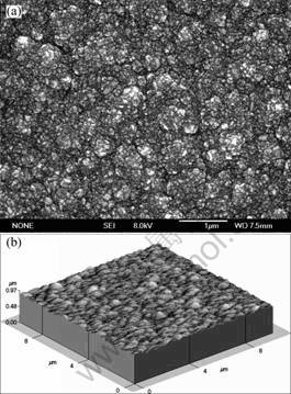
Fig. 1 Surface morphologies of nano-crystalline diamond film observed by SEM (a) and AFM (b)
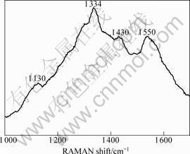
Fig. 2 RAMAN spectrum of nano-crystalline diamond film
cross-section of RAMAN scattering is 50-60 times higher for sp2 bonded carbon than that for sp3 bonded carbon, the concentration of non-diamond carbon impurities is rather low.
Spectroscopic ellipsometry (SE) is applied extensively in the field of optical thin film due to its multi-aspect merits such as high accuracy and sensitivity, processing convenience, and no-harm to samples as well. It is well known that thin films deposited on solid surfaces have very complicated microstructures. Since there are many lattice dislocations, grain boundaries and voids in the films, properties of these films are very different from their bulk counterparts. In ellipsometric analysis, a conventional method to simulate the optical variation of the film with deposition conditions is to model the film with a stack of layers having different compositions. Effective medium approximation (EMA) is the most frequently used approach to model the optical properties of polycrystalline thin films, which includes the grain boundary effect, voids, purity and surface roughness.
In this work, we also apply the Bruggeman EMA to model the phase purity and the surface roughness. The SE data, y and D, of the NCD film on Si substrate in the energy range of 0.75-1.50 eV are obtained. We analyze these experimental data using a model, Si|diamond+non-diamond|diamond+non-diamond+void|
air, to describe the structure of diamond film on silicon substrate (shown in Fig.3). The model consists of three layers, the bottom is silicon substrate, the top is the mixture of diamond and non-diamond phase, and the near surface is taken as another independent layer added voids phase again on account of the effect of its roughness.
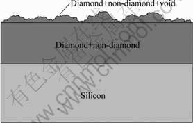
Fig.3 Schematic structure of nano-crystalline diamond film deposited on silicon based on model: Si|diamond+non-diamond
|diamond+non-diamond+void|air
The fitting results are listed in Table 1. A good fit is found between the model fit and experimental data. The standard deviation (s) is only 0.006 5. The overall thicknesses of the film, 2.212 mm, derived from the SE model are in agreement with that measured by SEM cross section measurement. The surface roughness (23.6 nm) obtained is slightly greater than the value (21.0 nm) obtained from AFM observation.
Table 1 Fitting results of diamond film on silicon substrate determined by SE measurements
Overall thicknesses of film/μm
Surface roughness/nm
Standard deviation
2.122
23.6
0.006 5
We employ the dispersion model for nano-crystalline materials proposed by FOROUHI and BLOOMER[13], which is derived on the basis of the extinction coefficient k for a single electron transition in the proximity of the interband energy gap (Eg):
 (1)
(1)
Unlike TAUC’s model, which is more commonly employed to evaluate the optical gap of amorphous semiconductors, the FB model does fulfill the causality principle [13], making it possible to arrive at the corresponding expression rigorously for the refractive index, n(E), through KRAMERS-KRONING relations:
 (2)
(2)
where Eg corresponds to the optical band-gap, n(?) is the refractive index at optical frequencies, A is inversely proportional to the lifetime of the excited states, and B is related to the energy difference between the bonding and anti-bonding states[13]. C depends on both A and B. Results for the optical constants n and k, obtained by calculating from the five parameters using Eqns.(1) and (2), are shown in Fig.4. The value of n varies little (2.361-2.366)in the given range of photo energy from 0.75 to 1.50 eV, nearing the ideal value of nature diamond (2.39). Being of the order of 10-2, the data of k also indicate a better transparency in this range.
The optical transmittance (T) of the NCD film isalso measured in a wavelength range from 200 nm to
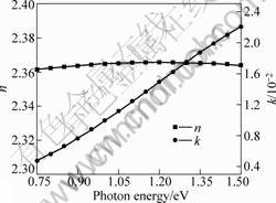
Fig.4 Calculated values of n and k of nano-crystalline diamond film
1 100 nm. The absorption coefficient (a) can be obtained by calculating from the following formula[14].
T=(1-R)2e-ad/(1-R2e-2ad) (3)
where d (2.212 mm) and R(0.24) are got from the ellipsometry spectroscopic analysis.
And the optical gap can be estimated from the following formula[12]:
ahn=B(hn-Eg)m (4)
where B is the proportionality factor, m is a parameter indicating the nature of optical transition in the film which is 2 for direct transition and 1/2 for indirect transition.
The value of m is difficult to define because of the existence of the mixed phases in the film having diamond crystallites (sp3) embedded in an amorphous non-diamond graphite phase (sp2). So, the optical gap is determined from the plots of (αhν)2 and (αhν)1/2 versus hν, respectively (shown in Fig.5). The estimated optical gap is 1.8 eV(m=2) and 4.3 eV(m=1/2). Obviously, the latter is more close to the value of natural diamond (5.5 eV). It seems that the direct transition may be the dominated mechanics for nano-crystalline diamond. As for the decrease of the optical gap, it is likely due to the augment of sp2 bonded phase among increasing grain boundaries.
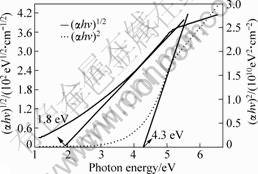
Fig.5 Energy gap under different transition mechanics
4 Conclusions
The structure, morphology and optical constants of the nano-crystalline diamond (NCD) film, deposited on silicon substrate by HFCVD method with the optimized deposition parameters, are investigated. SEM and AFM show that there is evident secondary nucleation and both the grain size and the surface roughness reach the order of nanometer. The RAMAN scattering spectrum shows there is more non-diamond phase in the film than conventional diamond films, but diamond phase is still the main portion. The measured SE data, y and D, of the nanocrystalline diamond film in the energy range of 0.75-1.50 eV are analyzed using a model, Si|diamond+non-diamond|diamond+non-diamond+void|
air, to describe the structure of diamond film on silicon substrate. By fitting the spectroscopic ellipsometric data with this model, the refractive index (n) of the NCD film varies little from 2.361 to 2.366 and the extinction coefficient (k) is of the order of 10-2. According to the data on the optical transmittance and absorption coefficient in the wavelength range from 200 to 1 100 nm, the optical gap of the NCD film is estimated to be 4.3 eV by a direct optical transition mechanics.
References
[1] GRUEN D M. Nanocrystalline diamond films[J]. Annu Rev Mater Sci, 1999, 29: 211-259.
[2] KULISCH W, POPOV C, BOYCHEVA S, BESHKOV G, VORLICEK V, GIBSON P N, GEORGIEV G. Investigation of the growth mechanism and structure of nanocrystalline diamond films by rapid thermal annealing[J]. Thin Solid Films, 2004, 469-470: 99-104.
[3] RAVET M F, ROUSSEAUX F Status of diamond as membrane materials for X-ray lithography masks[J]. Diamond Relat Mater, 1996, 5: 812-818.
[4] MCKENZIE D R, MULLER D A, PAITHORPE B A. Compressive-stress-induced formation of thin-film tetrahedral amorphous carbon[J]. Phys Rev Lett, 1991, 67(6): 773-776.
[5] DISCHLER B, BUBENZER A, KOIDL P. Bonding in hydrogenated hard carbon studied by optical spectroscopy[J]. Solid State Commun, 1983, 48: 105-108.
[6] NEMANICH R J, GLASS J T, LUCKOVSKY G, SHRODER R E. Raman scattering characterization of carbon bonding in diamond and diamond-like thin film[J]. J Vac Sci Technol A, 1988, 6(3): 1783-1787.
[7] ASPNSE D E, STUDN A A. Dielectric functions and optical parameters of Si, Ge, GaP, GaAs, GaSb, InP, InAs, and InSb from 1.5 to 6.0 eV[J]. Phys Rev B, 1983, 27: 985-1009.
[8] FALLON P J, VEERASWAMY V S, DAVIS C A, ROBERTSON J. Properties of filtered-ion-beam-deposited diamond-like carbon as a function of ion energy[J]. Phys Rev B, 1993, 48: 4777-4782.
[9] ROBERTSON J. Field emission properties of nanocrystalline chemically vapor deposited-diamond films[J]. Mater Res Soc Symp Proc, 1998, 509: 83-87.
[10] FANG Z J, XIA Y B, WANG L J, ZHANG W L, MA Z G, ZHANG M L. An ellipsometric analysis of CVD-diamond films at infrared wavelengths[J]. Carbon, 2003, 41:967-972.
[11] ZHANG M L, XIA Y B, WANG L J, GU B B, LOU Y Y. X-ray detectors based on (100)-textured CVD diamond films[J]. Phys Lett A, 2004, 332: 320-325.
[12] SUN Z, TAY B K, LAU S P. UV Raman characteristics of nanocrystalline diamond films with different grain size[J]. Diam Relat Mater, 2000, 9:1979-1983.
[13] FOROUHI A R, BLOOMER I. Optical dispersion relations for amorphous semiconductors and amorphous dielectrics[J]. Phys Rev B, 1986, 34: 7018-7026.
[14] SHARDA T, NUKAYA Y, SOGA T, JIMBO T, UMENO M. Structural and optical properties of diamond and nano-diamond films grown by microwave plasma chemical vapor deposition[J]. Diam Relat Mater, 2001, 10: 561-567.
(Edited by YANG You-ping)
Foundation item: Project(60577040) supported by the National Natural Science Foundation of China; Project(0404) supported by Shanghai Foundation of Applied Materials Research and Development; Projects(0452nm051, 05nm05046) supported by the Nano-technology Project of Shanghai; Project(T0101) supported by Shanghai Leading Academic Disciplines
Corresponding author: WANG Lin-jun; Tel: +86-21-56333514; Fax: +86-21-56332694; E-mail: ljwang@staff.shu.edu.cn

