
Microstructure and electrical properties of CeO2 ultra-thin films for MFIS FeRAM applications
TANG Ming-hua(唐明华)1, 2, ZHOU Yi-chun(周益春)1, 2, ZHENG Xue-jun(郑学军)1, 2,
WEI Qiu-ping(魏秋平)3, CHENG Chuan-pin(成传品)1, 2, YE Zhi(叶 志)1, 2, HU Zeng-shun(胡增顺)1, 2
1. Faculty of Materials and Optoelectric Physics, Xiangtan University, Xiangtan 411105, China;
2. Key Laboratory of Low Dimensional Materials and Application Technology, Ministry of Education, Xiangtan University, Xiangtan 411105, China;
3. School of Materials Science and Engineering, Central South University, Changsha 410083, China
Abstract: A detailed investigation about the dependence of microstructure and electrical properties on annealing temperature was carried out for cerium oxide(CeO2) ultra-thin films (18 nm to 110 nm) on n-type Si(100) substrates by RF magnetron sputtering. Substrate temperature was kept constant at 400 ℃ for all samples. The as-deposited films were subsequently annealed in air ambient at 700, 800 and 900 ℃ for 1 h respectively. The crystallinity and surface morphology of the CeO2 films were analyzed with X-ray diffractometer(XRD), scanning electron microscope(SEM), atomic force microscope(AFM) and Raman scattering measurement. Electrical properties of the Au/CeO2/Si/Au structure were examined by high frequency capacitance―voltage (C―V) characteristics at 1 MHz and leakage current density―electric field (J―E) characteristics. A Raman peak of the CeO2 thin films was seen at 463 cm-1. From C―V data, these films exhibit dielectric constants ranging from 18 to 23, the hysteresis width (ΔVFB) ranging from 0.015 V to 0.12 V and the density of trapped charges ranging from 1.45×10¹¹ to 3.01×1011 cm-2. A leakage current of 4.75×10⁻⁸ -9.0×10⁻⁷ A/cm2 at 2 MV/cm was observed. The experimental results show that the CeO2 buffer layers are suitable for non-volatile metal- ferroelectric-insulator-semiconductor(MFIS) structure field-effect-transistors(FETs) memory applications.
Key words: CeO2 thin film; RF magnetron sputtering; microstructure and electrical properties; MFISFETs memory applications
1 Introduction
Recently, ferroelectric random access memory (FeRAM) has attracted much attention because of its nonvolatile operation and high access speed[1-2]. FeRAMs are classified into two types. One is one transistor and one capacitor (1T-1C) type. The other consists of metal-ferroelectric-semiconductor field effect transistor (MFSFET, e.g. 1T type)[3-6]. Compared with the 1T-1C type, MFSFET has several advantages, such as nondestructive readout and decreasing memory cell size (e.g. high-density memory devices). However, MFSFET has serious problem such as the formation of an amorphous SiO2 layer with a low dielectric constant at the film/Si interface, highly trapped charge density and interdiffusion between the ferroelectric film and Si[7]. In order to solve these problems, a metal-ferroelectric- insulator-semiconductor(MFIS) structure was suggested by incorporating an insulator film as buffer layer between ferroelectric films and Si substrate[8]. For the applications of an insulator film to MFIS structure, several issues such as leakage current, capacitance, electrical breakdown, crystallinity, compatibility with Si, should be considered.
Among the available buffer materials, such as Al2O3, Y2O3, TiO2, ZrO2, HfO2, CeO2, and SrTiO3 [9-12], cerium dioxide (CeO2) with cubic fluorite structure (lattice parameter a0=0.541 1 nm) has been considered one of the most important insulating material because of its desirable properties such as chemical stability and close lattice parameter matching with silicon (lattice parameter a0=0.543 0 nm). Many physical deposition techniques, such as pulsed laser deposition(PLD)[13-14], magnetron sputtering[15], electron beam evaporation[16] and molecular beam epitaxy(MBE)[17], have been used to produce CeO2 films. Several chemical methods have also been applied, such as sol-gel[18], metallorganic chemical vapour deposition(MOVCD)[19], aerosol- assisted MOCVD[20], mist microwave-plasma chemical vapour deposition(MPCVD)[21], atomic layer deposition (ALD)[22] and spray pyrolysis[23].
In this work, CeO2 thin films (18-110 nm) were deposited by RF magnetron sputtering. Furthermore, the dependence of microstructure and electrical properties on annealing temperature of the CeO2 thin films was investigated.
2 Experimental
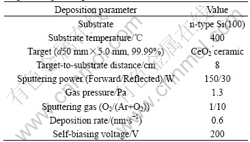
A 2-inch n-type Si(100) single crystal wafer with 6 Ω?cm resistivity was used as a substrate. The substrate was chemically cleaned using hot solutions (80 ℃) of φ(NH4OH)?φ(H2O2)?φ(H2O)(=1?1?5), and φ(HCl)? φ(H2O2)?φ(H2O) (=1?1?6), and 1% HF acid. After cleaning, CeO2 thin films were deposited on Si(100) substrates by RF magnetron sputtering method. The experimental conditions for CeO2 thin films deposition are listed in Table 1. In order to investigate the dependence of microstructure and electrical properties on annealing temperature, the as-deposited CeO2 thin films were annealed in air ambient for 1 h at 700, 800 and 900 ℃, respectively.
Table 1 Deposition conditions for CeO2 thin film by RF- magnetron sputtering
XRD (Panalytical X’pert, Holland) analysis was carried out using normal 2θ scanning method, and they were scanned at 10 (?)/min with degree increment of 0.018? with Cu Kα as the incident radiation (40 kV, 10 mA). Surface morphology of CeO2 thin films was recorded by AFM (Digital Instruments Nanoscpoe) and SEM (LEO-1530, Germany) with 50 K amplificatory. An HR 800 Raman spectrometer was conducted to study the lattice vibration modes. For electrical measurements, circular Au top electrodes (φ=0.2 mm) were sputtered on CeO2/Si structures through a stainless steel shadow mask and Au bottom electrodes on the backside of Si using dc magnetron sputtering. The high frequency C―V characteristics were measured using an impedance analyzer (Hewlett―Packard 4192A) at a measurement frequency of 1 MHz and signal amplitude of 10 mV with the sweep rate of 0.1 V/s. Using these C―V data, interface trap densities of CeO2/Si structures were calculated by the Terman method[24]. The leakage current density―electric field (J―E) characteristics were measured with HP4145B semiconductor parameter analyzer. All measurements were carried out at room temperature with 110 nm thick samples.
3 Results and discussion
Fig.1 shows the XRD patterns of CeO2 thin films on Si substrates annealed at different temperatures. The films consist of (111), (220) and (311) diffraction peaks corresponding to 2θ=28.6?, 47.5? and 56.3?, respectively, indicating that the samples are polycrystalline. No other peaks belonging to other phases are detected by XRD. The intensities of all peaks increase as the temperature increases. The Raman spectra of CeO2 thin films at different temperatures are shown in Fig.2. A well-resolved
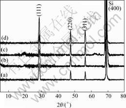
Fig.1 XRD patterns of CeO2 thin films annealed at different temperatures: (a) As-deposited; (b) 700 ℃; (c) 800 ℃; (d) 900 ℃
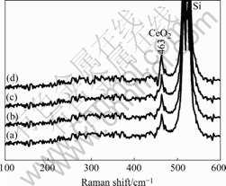
Fig.2 Raman spectra of CeO2 thin films annealed at different temperatures: (a) As-deposited; (b) 700 ℃; (c) 800 ℃; (d) 900 ℃
Raman peak of CeO2 thin film with grain size ranging from 20 to 41 nm is seen at 463 cm-1 in all samples, which is consistent with the result reported by WANG et al[25]. The intensity of peak increases slightly with increasing annealing temperature while the linewidth of peak has little change.
AFM and SEM have been employed to examine the surface morphology. Fig.3 corresponds to a typical 0.25 μm two-dimensional and three-dimensional images of CeO2 thin film annealed at 900 ℃. Fig.3 indicates that the microstructure of CeO2 thin film deposited directly on Si (100) substrate is granular structure with the surface roughness Rq=2.485 nm, the mean grain size is about 31.6 nm. As shown in Fig.4, the surface morphologies of CeO2/Si thin films observed by SEM are revealed to be flat and smooth, the grain size increases with increasing annealing temperatures.
Fig.5 displays the well-behaved high-frequency C―V characteristics of CeO2/Si structures annealed at different temperatures. A relatively little flat band voltage and small hysteresis width (ΔVFB) are observed in all samples and show larger windows of the hysteresis ranging from 15 mV to 120 mV as the annealing temperature increased from 700 ℃ to 900 ℃. The dielectric constant of the CeO2 thin films can therefore be determined from the measured value of accumulation capacitance(Cacc), using the relation
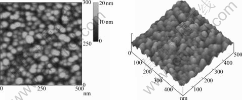
Fig.3 AFM images of CeO2 thin film annealed at 900 ℃
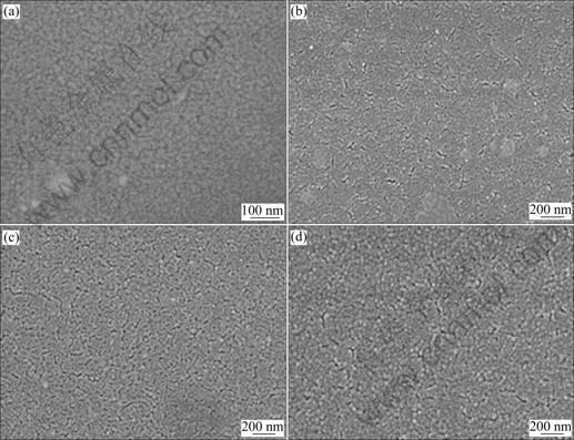
Fig.4 SEM morphologies for CeO2 thin films on Si(100) substrate annealed at different temperatures: (a) As-deposited; (b) 700 ℃; (c) 800 ℃; (d) 900 ℃
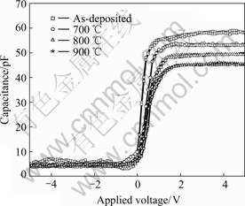
Fig.5 High frequency C―V characteristics upon different annealing temperatures
 (1)
(1)
where A is the area of capacitor(e.g. the electrode area), and d is the thickness of CeO2 dielectric layer. The obtained εr value at 1 MHz ranging from 18 to 23 decreases with increasing annealing temperature, indicating the growth of the interfacial amorphous SiO2 layer during annealing process. The equivalent oxide thickness (EOT) of CeO2 thin films can be calculated by
 (2)
(2)
where  =3.9 is the dielectric constant of SiO2, εr is the dielectric constant of CeO2 thin films, and d is the thickness of CeO2 thin films. The EOT increases from 18.6 nm to 23.8 nm as the annealing temperature increases. Note that for the above calculation, we ignored issues such as leakage current and reliability. In fact, actual performance of a complementary metal-oxide- semiconductor(CMOS) gate stack does not scale directly with the dielectric due to possible quantum mechanical and depletion effects[26].
Fig.6 illustrates the distribution of the four types charges: mobile ionic charge(Qm), oxide trapped charge (Qot), fixed oxide charge(Qf) and interface trapped charge (Qit). The density of these charges should be as low as possible for the performance and reliability of MFISFET device because the presence of these charges degrades significantly several key parameters such as the threshold voltage(Vth), transconductance, leakage current and breakdown voltage. The density of oxide trapped charges
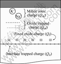
Fig.6 Distribution of four types charge in Au/CeO2/Si(100) structure
(Qot) can be quantitatively calculated from the C―V curves using following formula as
 (3)
(3)
where q is the electron charge. Qot increases from 1.74×10¹¹ to 1.09×1012 cm-2 as the annealing temperature increases. Using the C―V data shown in Fig.5, we also calculated the interface trapped charge density (Qit) by the Terman method:
 (4)
(4)
and
 (5)
(5)
where Cox is the CeO2 oxide capacitance per unit area, VG is the gate bias, ΦS is the surface potential, and CS is the silicon surface capacitance per unit area. The calculated interface trapped charge density (Qit) increases from 2.024×10¹² eV-1/cm2 to 3.453×10¹² eV-1/cm2 as the annealing temperature increases. We speculated that this observation may be due to the increase of the interface trapped charge density caused by increasing the internal stress in CeO2 thin films[24].
Fig.7 shows that the leakage current density of CeO2 thin films decreases with increasing annealing temperature. The observed leakage current density at an applied electric field of 2 MV/cm is 4.75×10⁻⁸ to 9.00×10⁻⁷ A/cm2, breakdown fields are measured as EBD≈3.5 MV/cm. The decrease of the leakage current level is due to the densification of the CeO2 thin films as well as the growth of the interfacial oxide layer.
In summary, all experimental results are listed in detail in Table 2 for integrity.
Table 2 Electrical parameters of MIS diodes with CeO2 dielectric layer (110 nm)
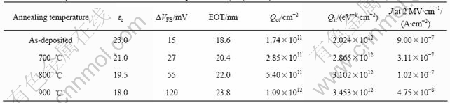
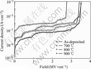
Fig.7 Leakage current density―electric field (J―E) charac- teristics upon different annealing temperatures
4 Conclusions
The dependence of microstructure and electrical properties on annealing temperature of CeO2 thin films deposited by RF magnetron sputtering were investigated as an insulator of the MFIS structure. All samples (18-110 nm) were polycrystalline, and showed stoichiometric CeO2 structure. The dielectric constant (εr) and leakage current density(J) decrease with the annealing temperature increasing, while the hysteresis width (ΔVFB), equivalent oxide thickness(EOT), oxide trapped charges density(Qot) and interface trapped charge density(Qit) increase with the annealing temperature increasing. Breakdown fields were about EBD≈3.5 MV/cm. The experimental results suggest that the CeO2 buffer layers are suitable for non-volatile MFISFET memory applications.
References
[1] SCOTT J F, ARAUJO C A. Ferroelectric memories [J]. Science, 1989, 246: 1400-1405.
[2] ARAUJO C A, CUCHIARO J D, MCMILLAN L D, SCOTT M C, SCOTT J F. Fatigue-free ferroelectric capacitors with platinum electrodes [J]. Nature, 1995, 374: 627-629.
[3] MOLL J L, TARUI Y. A new solid state memory resistor [J]. IEEE Trans Electron Devices, 1963, ED-10: 338-341.
[4] ISHIWARA H. Proposal of adaptive-learning neuron circuits with ferroelectric analog-memory weights [J]. Jpn J Appl Phys (Part 1), 1993, A32: 442-446.
[5] SUGIBUCHI K, KUROG Y, ENDO N. Ferroelectric field-effect memory device using Bi4Ti3O12 film [J]. J Appl Phys, 1975, 46: 2877-2882.
[6] ROST T A, LIN H, RABSON T A. Ferroelectric switching of a field-effect transistor with a lithium niobate gate insulator [J]. Appl Phys Lett, 1991, 59(27): 3654-3656.
[7] LEE H N, LIM M H, KIM Y T, KALKUR T S, CHOH S H. Characteristics of metal/ferroelectric/insulator/semiconductor field effect transistors using a Pt/SrBi2Ta2O9/Y2O3/Si structure [J]. Jpn J Appl Phys (Part 1), 1998, 37: 1107-1109.
[8] PARK B E, ISHIWARA H. Electrical properties of LaAlO3/Si and Sr0. 8Bi2.2Ta2O9/LaAlO3/Si structures [J]. Appl Phys Lett, 2001, 79(6): 806-808.
[9] HOUSSA M, TUOMINEN M, NAILI M, AFANAS’EV V, STESMANS A, HAUKKA S, HEYNES M M. Trap-assisted tunneling in high permittivity gate dielectric stacks [J]. J Appl Phys, 2000, 87: 8615-8620.
[10] COPEL M, GRIBELYUK M A, GUSEV E. Structure and stability of ultrathin zirconium oxide layers on Si(001) [J]. Appl Phys Lett, 2000, 76(4): 436-438.
[11] OHSHITA Y, OGURA A, HOSHINO A, HIIRO S, MACHIDA H. HfO2 growth by low-pressure chemical vapor deposition using the Hf(N(C2H5)2)4/O2 gas system [J]. J Cryst Growth, 2001, 233: 292-297.
[12] LEE B H, KANG L, NIEH R, QI W, LEE J C. Thermal stability and electrical characteristics of ultrathin hafnium oxide gate dielectric reoxidized with rapid thermal annealing [J]. Appl Phys Lett, 2000, 76(14): 1926-1928.
[13] WU X D, DYE R C, MUENCHAUSEN R E, FOLTYN S R, MALEY M, ROLLETT A D, GARCIA A R, NOGAR NS. Epitaxial CeO2 films as buffer layers for high-temperature superconducting thin films [J]. Appl Phys Lett, 1991, 58: 2165-2167.
[14] DENHOFF M W, MCCAFFREY J P. Epitaxial Y1Ba2Cu3O7 thin films on CeO2 buffer layers on sapphire substrates [J]. J Appl Phys, 1991, 70(7): 3986-3988.
[15] WANG F, WORDENWEBER R. Large-area epitaxial CeO2 buffer layers on sapphire substrates for the growth of high quality YBa2Cu3O7 films [J]. Thin Solid Films, 1993, 227(2): 200-204.
[16] MAUL M, SCHULTE B, HAUSSLER P, FRANK G, STEINBORN T, FUESS H, ADRIAN H. Epitaxial CeO2 buffer layers for YBa2Cu3O7-δ films on sapphire [J]. J Appl Phys, 1993, 74(4): 2942-2944.
[17] PARK B E, SAKAI I, TOKUMITSU E, ISHIWARA H. Hysteresis characteristics of vacuum-evaporated ferroelectric PbZr0.4Ti0.6O3 films on Si (111) substrates using CeO2 buffer layers [J]. Appl Surf Sci, 1997, 117: 423-428.
[18] CELIK E, SCHWARTZ E J, AVCI E, SCHNEIDER-MUNTAU H J, HASCICEK Y S. CeO2 buffer layers for YBCO: Growth and processing via sol-gel technique [J]. IEEE Trans Appl Supercond, 1999, 9: 2264-2267.
[19] GRABOY I E, MARKOV N V, MALEEV V V, KAUL A R, POLYAKOV S N, SVETCHNIKOV V L, ZANDBERGEN H W, DAMHMEN K H. An improvement of surface smoothness and lattice match of CeO2 buffer layers on R-sapphire processed by MOCVD [J]. J Alloys Compd, 1997, 251: 318-321.
[20] FROHLICH K, SOUC J, ROSOVA A, MACHAJDIK D, GRABOY I E, SVETCHNIKOV V L, FIGUERAS A, WEISS F. Superconducting YBa2Cu3O7 films prepared by aerosol metal organic chemical vapour deposition on Al2O3 substrate with CeO2 buffer layer [J]. Supercond Sci Technol, 1997, 10: 657-662.
[21] TAKAHASHI N, KOUKITU A, SEKI H. Growth and characterization of YBa2Cu3Ox and NdBa2Cu3Ox by mist microwave-plasma chemical vapor deposition using a CeO2 buffer layer [J]. J Mater Sci, 2000, 35: 1231-1238.
[22] PAIVASAARI J, PUTKONEN M, NIINISTO L. Cerium dioxide buffer layers at low temperature by atomic layer deposition [J]. J Mater Chem, 2002, 12: 1828-1832.
[23] ELIDRISSI B, ADDOU M, REGRAGUI M, MONTY C, BOUGRINE A, KACHOUANE A. Structural and optical properties of CeO2 thin films prepared by spray pyrolysis [J]. Thin Solid Films, 2000, 379: 23-27.
[24] TERMAN L M. An investigation of surface states at a silicon/silicon oxide interface employing metal-oxide-silicon diodes [J]. Solid-State Electron, 1962, 5(5): 285-299.
[25] WANG S Y, WANG W, ZUO J, QIAN Y T. Study of the Raman spectrum of CeO2 nanometer thin films [J]. Materials Chemistry and Physics, 2001, 68: 246-248.
[26] RIOS R, ARORA N D. Tech Dig 1994 IEEE Int Electron Devices Meet [C]. San Francisco, 1994: 613.
(Edited by PENG Chao-qun)
Foundation item: Project(076044) supported by the Cultivation Fund of the Key Scientific and Technical Innovation Projects, Ministry of Education of China; Project(KF0602) supported by the Open Project Program of LDMAT (Xiangtan University), Ministry of Education, China
Corresponding author: ZHOU Yi-chun; Tel: +86-732-8293586; E-mail: zhouyc@xtu.edu.cn

