
Method of surface treatment on sapphire substrate
NIU Xin-huan(牛新环), LIU Yu-ling(刘玉岭), TAN Bai-mei(檀柏梅),
HAN Li-ying(韩丽英), ZHANG Jian-xin(张建新)
Institute of Microelectronic, Hebei University of Technology, Tianjin 300130, China
Received 10 April 2006; accepted 25 April 2006
Abstract: Sapphire single crystals are widely used in many areas because of the special physic properties and important application value. As an important substrate material, stringent surface quality requirements, i.e. surface finish and flatness, are required. The use of CMP technique can produce high quality surface finishes at low cost and with fast material removal rates. The sapphire substrate surface is treated by using CMP method. According to sapphire substrate and its product properties, SiO2 sol is chosen as abrasive. The particle size is 15-25 nm and the concentration is 40%. According to the experiment results, pH value is 10.5-11.5. After polishing and cleaning the sapphire surface, the surface roughness was measured by using AFM method and the lowest value of Ra 0.1 nm was obtained. From the results, it can be seen that using such method, the optimal sapphire surface can be gotten, which is advantageous for epitaxial growth and device making-up.
Key words: sapphire; substrate; surface treatment; chemical mechanical polishing; slurry
1 Introduction
Sapphire (α-Al2O3) single crystal combines many good mechanical and optical properties[1,2] that make it become the material of choice in a variety of modern Hi-Tech applications such as space and military optical systems, high-power laser optics, blue emitting diodes, laser diode devices, visible-infrared windows, substrates for semiconductor devices and high-pressure components. In addition, (0001) sapphire crystal wafers can be used as substrates for growing photoelectric materials-GaN thin films[3]. Sapphire wafer is also widely used for GaN-based Ⅲ-nitride device fabrication [4]. In many of these applications, stringent surface quality requirements (i.e., finish and flatness) are required. The generation of high-quality surfaces with fine surface finish and low surface and subsurface damage is also critical importance. It has been established that the crystal structure of epitaxial films is strongly influenced not only by the substrate material and its orientation, but in a great extent also by the surface preparation of the substrate[5]. Fine surface machining and polishing of ceramics for opto-electronic applications may exceed 80% of total cost. The use of chemically assisted polishing techniques such as chemical mechanical polishing (CMP) may produce high quality surface finishes at low cost and with fast material removal rates [6]. CMP has been widely and effectively applied to a variety of materials in last two decades, including semiconductors, crystals, glasses, special metals, plastics and computer disks. CMP is becoming popular because the advantages of CMP over other surface finishing techniques are great: little or no surface and subsurface damage, elimination of surface defects, high removal rates, high efficiency, and low cost[7-10]. However, many ceramics such as sapphire are noted for wear and corrosion resistance due to the high chemical and thermal stability, high hardness and in many cases the effective CMP processes are not available or not understood[11-13]. In this study, according to basic reaction mechanisms we treated the sapphire substrate by CMP method using a new-type slurry and obtained high removal rate and low roughness.
2 Experimental
In this study, the sapphire crystals were obtained by Czochralski (Cz) method. The diameter is 50 mm. The crystals were grown by using a [0001] direction seed under a high pure flowing Argon gas atmosphere with a pulling rate of 1.5-2.0 mm/h and a rotation rate of 10-30 r/min.
After being edge rounded, sapphire crystal wafers with thickness of 0.4 mm for test were cut perpendicular to the growth direction from the equant section of crystal-bar. The surfaces were lapped using diamond powders and polished by chemical mechanical polishing(CMP) method on C6382I-W/YJ polisher. After cleaning the samples, we measured the surface roughness on Nanoscope Ⅲa Multimode. The abrasive size was measured by Mastersizer 3000HS particle size analyzer.
3 Result and discussion
3.1 Selection of media
Chemical mechanical polishing(CMP) is the combination technique of mechanical grinding and chemical corrosion. During the polishing process, it includes chemical reaction kinetics process and mass transmission process. Fig.1 shows the schematic illustration of a CMP system.
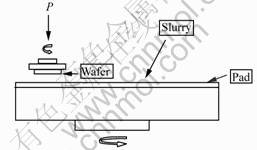
Fig.1 Schematic illustration of CMP system
During the sapphire substrate CMP process, under the alkali media the chemical reactions are as follows[6]:
 (1)
(1)
 (2)
(2)
 (3)
(3)
 (4)
(4)
First α-alumina reacts with H2O and forms the hydrates of α-alumina[6], and the hardness of such hydrates is lower than α-alumina. At the same time, a part of substrate material and hydrates react with alkali, and form water soluble . Alumina is an amphoteric oxide, so it can react with acid, also react with alkali. In this study, we chose alkali media, the reasons are as follows: First alkali has passivating action, so it can avoid etching equipment. Second, if we choose acid media, there will be the reactions as follows:
 (5)
(5)
 (6)
(6)
 (7)
(7)
From the above chemical formula we can see that alum ion can be formed, which causes ionic secondary pollution. It takes more difficult for cleaning. Third, alkali media takes important action for abrasive stability.
3.2 Selection of abrasive
During the sapphire substrate polishing, we should select the abrasive according to the reaction products hardness, but not according to substrate material hardness. On the study of sapphire substrate CMP, Al2O3 and corundum were always selected as abrasive in last years. But corundum hardness is higher than substrate, then it is easy to cause surface scuffing. Although the substrate surface quality is better than the former using Al2O3 as abrasive, Al2O3 is easy to react with alkali and the reaction product is soluble, which can cause the abrasive concentration to decrease and the particle size to be inconsistent (Fig.2). From Fig.2 it can be seen that there appears inactive abrasive, which causes active abrasive concentration to decrease. So it will influence removal rate and cause surface or subsurface damage. According to the above reasons, we chose nano-silica as abrasive. Silica abrasive was more stable in proper alkali environment, and the hardness was close to substrate material hydrates. According to the experiment results, we chose the concentration of silica abrasive was 40%, and the particle size was 15-25 nm. From our investigation, we found that abrasive took the action of agitator and mechanical grinding. During polishing process, abrasives took the action of transmitting reactant and reaction products. High concentration and small particle size caused silica abrasive little dispersion degree (Fig.3, silica abrasive TEM photograph), which was advantageous to removal rate and surface quality.
3.3 Select of pH value
pH value is an important factor during CMP process. It takes important action on chemical reaction of CMP
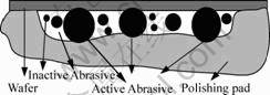
Fig.2 Schema of polishing of abrasive with different particle sizes in non-contact area
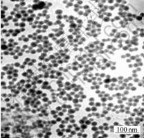
Fig.3 TEM photograph of 15-25 nm silica abrasive
process, and it must ensure the stability of silica abrasive. As usual, higher pH value is advantageous to chemical reaction. With pH value rising, the stability of silica abrasive will be lower. When pH value reaches a certain value, silica abrasive will begin to aggregate. The aggregates can cause polishing pad jamming, which influences the slurry transmitting. Then it causes chemical reaction to be slower, removal rate to decrease and surface quality to be lower. According to our experiment results, the pH value range is 10-12, which can ensure the floatability of silica abrasive in slurry and high removal rate.
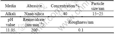
After polishing and cleaning, the substrate surface was measured by AFM (Fig.4). Under the optimal processing parameter (Table1), the surface roughness can reach 0.1 nm.
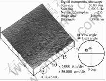
Fig.4 AFM morphology of sapphire wafer surface polished with silica nano-scale abrasive
Table 1 Sapphire substrate CMP optimal parameters
4 Conclusion
According to sapphire substrate material property and CMP mechanism, nano-silica was chosen as the sapphire substrate CMP abrasive. The particle size was 15-25 nm, and abrasive concentration was 40%. It was found that high concentration and small particle size ensured silica abrasive little dispersion degree, which was advantageous to removal rate and surface quality. Alkali media took passivating action on polishing equipment, and proper alkali environment ensured silica abrasive stability. At the pH value in the range of 10-12, the higher removal rate and good surface quality were abstained. Different material CMP technique should have different theoretical model. So the next step work is to investigate sapphire substrate CMP theoretical model and optimize process parameter.
References
[1] DOLGAEY S I, LYALIN A A, et al. Fast etching of sapphire by a visible range quasi-cw laser radiation[J]. Applied Surface Science, 1996, 96-98: 491-496.
[2] JIHONG L I, NUTT S R, KIRBY K W, et al . Surface modification of sapphire by magnesium ion implantation[J]. J Am Cerum Soc, 1999, 82(11): 3260-3264.
[3] NELTON W A, PANKOVE J I. GaN growth on sapphire[J]. Journal of Crystal growth, 1997, 178: 168-172.
[4] HSU Y P, ChANG S J, SU Y K. ICP etching of sapphire substrates[J]. Optical Materials, 2005, 27: 1171-1174.
[5] WANG Yin-zhen, PENG Guang-liang, LIU Shi-liang, et al. Influence of Surface treatment on the sapphire substrate[J]. Journal of Synthetic Crystals, 2005, 34(3): 431-434.(in Chiense)
[6] ZHU Hong-lin, TESSAROTO L A. Chemical mechanical polishing(CMP)anisotropy in sapphire[J]. Applied Surface Science, 2004, 236: 120-130.
[7] HARA T, BALAKUMAR S. Chemical mechanical polishing of copper layer employing MnO2 slurry[J]. Thin Solid Films , 2004, 462-463: 186-191.
[8] BORST C L, KORTHUIS V, SHINN G B. Chemical-mechanical polishing of SiOC organosilicate glasses: the effect of film carbon content[J]. Thin Solid Films , 2001, 85: 281-292.
[9] LEI Hong, LUO Jian-pin. CMP of hard disk substrate using a colloidal SiO2 slurry: preliminary experimental investigation [J]. Wear, 2004, 257: 461-470.
[10] FORSBERG M. Effect of process parameters on material removal rate in chemical mechanical polishing of Si(1 0 0)[J]. Microelect-
ronic Engineering , 2005, 77: 319-326.
[11] HAHN P O. The 300 mm wafer-a cost and technology challenge[J]. Microelectronic Engineering, 2001, 56: 3-13.
[12] WANG Xiao-hui,LIU Xian-liu,WANG Du, et al. Chemical polishing of sapphire for growth of GaN[J]. Chinese Journal of Semiconductors, 1997, 18(11): 867-871.( in Chinese)
[13] LI Bing, GUO Xia, LIU Ying, et al. Study on the back lapping and polishing of sapphire-based LED epitaxial wafers[J]. Semiconductor Technology, 2005, 39(9): 57-60.(in Chinese)
(Edited by CHEN Ai-hua)
Foundation item: Project(043801211) supported by the Tianjin Natural Science Foundation; Project(20050080007) supported by the Specialized Research Fund for the Doctoral Program of Higher Education of China
Correspondence: NIU Xin-huan; Tel: +86-22-26564424; E-mail: xingguojia@eyou.com

