模式可配置的NAND Flash纠错系统设计与实现
徐富新,刘应,刘雁群,向超
(中南大学 物理与电子学院,湖南 长沙,410083)
摘要:针对NAND flash存储器设计一种模式可配置的纠错系统的电路结构,该结构可以预防错误位数大于设计纠错位数的情况发生。提出一种高速并行BCH编译码的电路设计方法,并导出一种无需有限域求逆运算的BM迭代算法的硬件实现方法。通过复用编码算法电路与译码算法电路,同时结合流水线技术与乒乓操作技术,实现以较小的硬件资源开销提高纠错系统性能。该纠错系统电路在EP4CE15E22C8系列FPGA芯片上实现,并进行测试分析。测试结果表明:在相同的系统工作频率下,该纠错系统电路的数据吞吐率是传统串行纠错电路的8倍,而硬件资源开销只增加1倍;与传统的NAND flash纠错电路相比,该纠错电路结构相对独立,可移植性强,可满足多种应用场合的需要。
关键词:Nand flash存储器;纠错电路;可配置模式;BCH码;现场可编程门阵列
中图分类号:TP919.3 文献标志码:A 文章编号:1672-7207(2013)05-1918-08
Design and implementation of mode reconfigurable NAND flash error correcting system
XU Fuxin, LIU Ying, LIU Yanqun, XIANG Chao
(School of Physics and Electronics, Central South University, Changsha 410083, China)
Abstract: Mode reconfigurable error correcting circuit was presented for NAND flash memory. This circuit can effectively avoid larger error bits than the designed error correcting bits. Hereinafter, a circuit design method of parallel BCH code was brought up, and a kind of BM iterative algorithm hardware implementation was deduced without finite field inverse operation. Based on the multiplexing technology of the codec algorithm circuit and combing pipeline technology with ping-pong operation technology, the performance of the correcting system is improved ingeniously while the increase of the cost is acceptable. The error correcting system circuit is implemented and tested in the FPGA chip of the EP3CE15E22C8 series. Under the same system operating frequency, eight times greater data throughput rate are achieved than those of the traditional serial circuits with only double hardware cost. In comparison with traditional NAND flash error correcting circuit, the present error correcting circuit is relatively independent and portable, and can meet the requirement of several applications.
Key words: NAND flash memory; error correction circuit; reconfigurable mode; BCH code; FPGA
NAND flash存储器具有容量较大、读写速度快、无噪音、使用方便等优点,适用于大量数据的存储,在业界得到广泛应用。但由于NAND flash 存储密度大,每个存储单元之间的距离很小,存储单元产生漏电的现象不可避免[1-2],有可能导致写入存储单元的数据与读出来的数据不一致,而且易产生坏块,因此,在对NAND flash进行数据存储时,必须采用前向纠错技术,以提高数据存储的稳定性[3]。随着NAND flash广泛使用,对NAND flash的纠错设计也成为当前的研究热点。纠错编码在通信中应用较多,但在数据存储领域中的应用研究并不多。由NAND flash的错误特征与汉明重量的关系[4]推导出的纠错电路实现简单,但只能够纠正1位错误。采用里德-所罗门码(reed-solomon code)设计的纠错电路[5-6]可以实现对非二进制数操作,但电路复杂且硬件资源开销大。Bose-Chaudhuri-Hocquenghen (BCH)编译码电路可纠正多位随机错误,且速度快,电路简单,因而得到广泛研究[7-8]。BCH编译码电路的难点是译码电路的设计。欧几里德译码法一般可以采用脉动阵列实现译码电路[9-10],但同样存在硬件资源开销大的缺点。经典的Berlekamp-Massey(BM)译码法是应用最广的BCH译码法,但在译码过程中需要进行迭代运算与有限域求逆运算,电路实现比较复杂[11-12]。逐步译码法也是一种应用比较多的译码法[13],电路简单,但译码时间长,不能满足高速系统的要求。为此,本文作者从NAND flash应用的整体考虑,设计一个易于实现的低复杂度、模式可配置的纠错系统电路,并结合流水线技术、乒乓操作技术、表达式共享技术来提高纠错系统的综合性能。
1 系统总体结构设计
与以往设计中纠错部分隶属于NAND flash控制器不同,本文将纠错功能单独设计,纠错系统与NAND flash控制器采用流水线式的工作方式,以提高数据吞吐率与功能模块的可移植性。编码与NAND flash的写操作重叠进行,译码的第1级流水线与NAND flash的读操作重叠进行,第2级流水线与译码数据输出同时进行,通过减少流水线的级数来减少编译码带来读写NAND flash时间的增加。NAND flash纠错系统由纠错控制模块、编译码模块、自动重写判断模块以及读写乒乓缓冲模块组成。纠错系统的总体结构如图1所示。
整个纠错系统电路的输入为上层控制信号与原始数据,输出为状态信号与译码后的数据。编译码模块是纠错设计的重点与难点,该模块直接影响整体的数据吞吐率。
考虑到在大容量存储应用中,一般为多通道NAND flash并行工作,为了减少编译码的延时,在编译码前分别设计了乒乓缓冲模块。NAND flash以页为单位进行读写操作,每一页的数据量为4 096 bit,数据总线为8位宽,因此,乒乓缓冲模块由2个512字节RAM组成,使得编译码模块可以连续工作,提高系统吞吐率。
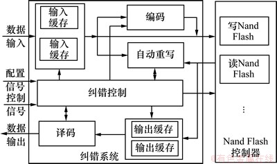
图1 纠错系统结构
Fig.1 Structure of error correction system
纠错电路只能纠正错误位数小于等于编译码设计的纠错位数的情况。为了提高纠错系统的整体性能,引入通信中的自动重传策略[14],设计1个自动重写判断模块来判断数据写入NAND flash是否满足要求。
控制模块实现对纠错系统中各个模块工作状态的控制并输出相应的状态信号。控制模块接收输入的配置参数后,设定纠错系统的工作模式,并根据控制信号启动相应的模块工作。根据NAND flash的不同应用场合,可以配置不同的纠错模式,配置方式如表1所示。
表1 纠错模式配置
Table 1 Mode configuration of error correction
2 并行BCH编译码设计
BCH码是1种可纠正多个随机错误的循环码,因其电路实现比其他纠错码简单,因此,BCH码被广泛应用于纠错系统中。传统的BCH编译码电路采用串行方式工作,显然在很多场合不能满足系统对数据吞吐率的要求。BCH编码电路相对简单,只需要计算校正位即可。BCH译码电路较复杂,译码纠错需由3步组成:第1步为计算校正子(si),第2步为确定错误位置多项式σ(x),第3步为求解错误位置数并纠错。由于本文设计的4种纠错模式(见表1)都是在同一有限域内运算,因此,码字中只有校验位的长度不同,可以设置校验位寄存器的长度为最大值13字节,工作时通过配置信号来选择相应长度,这样,在各个模式下即可共用编码电路与校正子计算电路。求解错误位置数电路是对同样的信息位进行操作,因此,各个模式下该模块完全相同。不同的纠错模式确定错误位置多项式的电路是不同的,但设计方法相同。下面以纠4 bit错为列,讨论并行BCH编译码电路的设计。
2.1 并行BCH编码设计
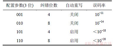
构造BCH(n, k, t)码,需要确定3个关键参数,即码长n、信息位k、纠错力t。NAND flash以按页的方式存储,每页的数据为4 096 bit。以(4 148,4 096,4) BCH码为例,其码长为4 148 bit,信息位为4 096 bit,纠错能力为4 bit,它是本原(8 191,8 139,4) BCH码的缩短码,以x为变量,则它的生成多项式g(x)为
g(x)=x52+x50+x46+x44+x41+x37+x36+x30+x25+x24+x23+x21+x19+x17+x16+x15+x10+x9+x7+x5+x3+x1+1 (1)
BCH的码字由信息位与校验位组成,信息位在高位,校验位在低位。校验位即为信息位除以生成多项式的余数。设v(x)表示信息位,则BCH码字u(x)可由下式求得:
 (2)
(2)
式中: 表示
表示 除以
除以 得到的余数;
 表示4 096 bit的信息位,即为52 bit的校验位。
传统的串行编码电路需要4 096个时钟计算,即第4 096时刻的余数寄存器的值为校正子。设矩阵 表示当前t时刻余数寄存器的值,矩阵
 为8位并行输入信号,矩阵
 为1个与有关的系数矩阵,则t+1时刻余数寄存器的值为:
 (3)
(3)
通过对式(3)的迭代运算可以求出第8时刻 的余数寄存器的值与当前余数寄存器的值以及输入之间的关系。由得到的关系式即可设计出8位并行的编码电路,其编码电路如图2所示。图2中:b[7:0]为8位并行输入的信息位数据;a[51:0]和c[51:0]分别表示前时刻与下一时刻校验位寄存器的值。编码电路经过512个时钟的计算即可以得到校验位,在计算校验位的512个时钟内同时输出码字的信息位,并在接下来的7个时钟内由高位到低位依次输出码字的校验位,完成编码。
2.2 并行BCH译码设计
BCH译码纠错过程由3步组成:计算校正子(si);确定错误位置多项式σ(x);求解错误位置数并纠错。校正子计算电路的设计方法与编码电路设计方法相似,下面重点讨论后2个电路的实现。
2.2.1 错误位置多项式推导电路
每一种求解错误位置多项式的方法即为1种译码算法,在众多的译码算法中,以Berlekamp与Massey提出的BM迭代译码算法使用最多。BM迭代算法因效率高且具有最简单的硬件实现结构而得到广泛应用。BM算法是根据校正子来确定错误位置多项式 的系数(其中,u为迭代次数;
 和
和 分别为
分别为 的次数与系数)。令
 为当前值与上一步迭代值之差。BM算法的迭代步骤为:令初始值
 ,
, ,
, ,
, ,若
,若 ,则
,则 不改变,为
不改变,为 ,否则,
,否则, (其中,
(其中, 为第u次之前差值不为0的迭代次数)。显然,要直接在硬件上实现上述迭代运算,电路很复杂。根据BM迭代的特点,针对纠错位数较小的情况,推导出一种基于BM算法、无需在硬件上迭代求逆的直接树判决法[15]求解错误位置多项式。纠4 bit错的直接树判决法示意图如图3所示。
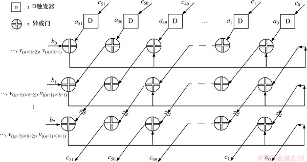
图2 并行编码电路
Fig.2 Circuit of parallel encoder
图3中:方框中的值表示当前步数的迭代值;K,M,N,O,P,Q,R和T表示当前节点du的值。可知纠4 bit纠错直接判决树法,只需要求出A,B,C,D,E,F,G,H和I这9个多项式。err表示超出纠错范围的错误。由于设计了校正子全为零(无错)时不会启动该模块,因此,最左边的2条路径可以简化,而只需要判断右边的13条路径。由BM迭代法,预先求出判决树上每一个节点的表达式,而在硬件上只需要执行相对应的有限域乘法与加法运算,因此,整个复杂的BM迭代电路转变为根据各个节点的值选择错误位置多项式所在路径的状态控制电路。
现以求多项式H为例,推导无求逆算法。当满足 ,
, ,
, 和T=0时,由BM迭代法可以求得此时的错误位置多项式为
 (4)
(4)
同时,可由BM算法求得: ;
; 。又因
。又因 ,所以,节点Q的判决条件可以修改为:
 ,,且多项式方程乘1个常系数其根不变,因此,可以化解G中的求逆运算,得到无求逆的多项式:
 (5)
(5)
通过同样的方法可以得到其他路径的无求逆多项式。采用直接树判决法只需要3个有限域乘法器与2个有限域加法器即可以在10个时钟内完成求解错误位置多项式。并且整个运算过程采用流水线结构,减小了关键路径的延时。对于纠8 bit错的情况,同样可以采用直接树判决法,只需要增加5个有限域乘法器与1个9输入的有限域加法器便可以在26个时钟内完成纠8 bit错误情况下的求解错误位置多项式。
2.2.2 求解错误位置数与纠错
求解错误位置数就是将有限域上全部的域元素代入错误位置多项式σ(x)以确定其根。求解错误位置数的方法有多种,本文采用钱氏(Chien)搜索电路实现求解错位位置数,并结合应用进行相应优化设计。传统的串行钱氏搜索电路每个时钟搜索1个元素,纠4 bit错的钱氏搜索电路需要4个有限域乘法器和1个有限域加法器。为了提高搜索速度,必须设计1个时钟可以搜索多个位置的并行钱氏搜索电路。
图4所示为8位并行搜索电路。由于本文使用的BCH码(4 148,4 096,4),它是本原BCH码(8 191,8 139,4)的缩短码,即信息位的高4 043位全为0;又因在输出校验位时在最后补了4位0,因此,信息位的第1个元素为有限域的第4 040个元素,将错误位置搜索的起点设置为第4 040个元素即第1个输入信息位,可节省约一半的搜索时间。在硬件实现时,采用乘以有限域元素a4 039跳过确定的非错误位置,以保证由第1个信息位开始搜索错误位置。在接下来的512个时钟内将每一个元素代入σ(x)并判断表达式的值,若σ(x)为0,则当前位置即为错误位置。图4中:σ1,σ2,σ3和σ4为σ(x)系数; ,
, ,
, 和
和 为钱氏搜索运算中的累乘值。经过512个时钟即能完成对信息位的搜索。因错误位置是随机分布的,通过图4中的控制电路对搜索到的错误位置数计数,当计数等于错误个数时即完成搜索,由概率统计可知:加入控制电路后能平均减少一半的搜索时间,降低搜索电路的功耗。
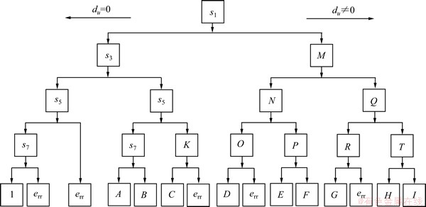
图3 直接树判决法
Fig.3 Method of direct tree verdict
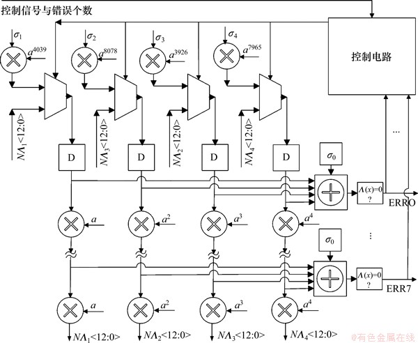
图4 并行钱氏搜索电路
Fig.4 Circuit of parallel Chien search
由于译码的第1步需要519个时钟周期,第2步需要10个时钟周期,第3步需要512个时钟周期,因此,译码器采用2级流水线:第1级流水线计算校正子,第2级流水线求解错误位置多项式方程并搜索错误位置数。
本文采用读译码器输出数据与钱氏搜索重叠工作的方法,减少整个数据读操作中的流水线级数,提高译码的工作效率。在搜索出数据错误位置的同时,将其转换为对应数据在输出缓冲中的存储地址,并对该存储地址中的数据纠错,输出译码后的正确数据。
3 自动重写判断
当发生的错误位数大于设计的纠错位数时,传统的译码电路不能够纠正错误。为了防止这种情况发生,本文设计1个自动重写判断模块,以弥补编译码器功能的不足,同时也有利于对NAND flash的坏块管理。自动重写判断模块由纠错系统控制模块发出的控制信号设定工作状态,可以配置为启用或者关闭状态。其电路原理如图5所示。其工作原理是将编码后的数据写入NAND flash后,从NAND flash读出信息位与原始数据进行异或运算,由异或运算的结果判断发生错误的位数。当出现错误位数大于设计的纠错位数时,立即停止比较并发出自动重写信号,重新将数据写入另外的页;当发生错误的个数小于设计的纠错位数时,则一直比较完512个字节,并发出写入成功信号。该简单的电路能使误码率大大降低,但不能够对单块NAND flash进行连续写操作。而在对多块NAND flash进行写操作时,采用乒乓操作技术,即能实现连续写操作。
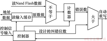
图5 自动重写判断
Fig.5 Judgment of automatically rewrite
4 仿真与验证
本文设计的纠错系统电路使用verilog语言完成RTL级设计,使用Quartus软件完成电路综合,同时使用ModelSim和SignalTap软件进行时序分析与验证。图6~8中:clk_50m为纠错系统电路的系统时钟;cur_state为求解错误多项式的状态机;M,Q和T为前面推导的各节点du;bm_en为求解错误多项电路使能信号;chien_en为钱搜索电路使能信号;buf_dinb和buf_addr分别为输出缓存的数据与数据地址;rErr_addr,Err和Err_data号则分别为错误地址、纠错标志、错误校正数据;DecData为译码输出数据。
图6所示是配置为纠4 bit错是的译码仿真时序图。由图6可知:译码电路接收到使能信号则开始译码,当计算完4个校正子(s1,s3,s5和s7)的值,若其中任意校正子等于0,则直接结束译码,否则,使能求解错误位置多项式电路。经过10个时钟计算出错误位置多项式的系数后,立即使能钱搜索电路(chien_en为高电平)。钱搜索电路每个时钟同时搜索8个位置。搜索到错误位置后,并根据计算出校验数据,对错误数据纠正。图6所示为在信息位的第3个到第6个字节上各发生1bit错的情况。
图7所示是纠错系统电路配置为纠8 bit错时的译码仿真时序图。其译码步骤与纠4 bit错时相同。计算8个校正子(未在图中给出),其值分别为:s1=0 978h(用h表示16进制),s3=1 864h,s5=0A2Fh,s7= 0FCCh,s9=1175h,s11=15D1h,s13=0B8Ch,s15=0673h。因有校正子不等于0,故开始计算错位位置多项式。当发生8 bit错时,需要26个时钟计算错误位置多项式系数p0~p8(未在图中给出),其值分别为p0=1936h,p1=144Dh,p2=12ECh,p3=DE50h,p4=0595h,p5=0316h,p6=0CA7h,p7=0069h,p8=1F3Ch。上面8个校正值与9个错误位置多项式的系数是由图7中的数据计算而来的。图7中,在信息位的第2个字节搜索到错误,立即使能纠错标志信号(rErr为高电平),同时计算校验数据0Fh,并纠正错误位,得到译码输出数据3Fh;当搜索到第12个信息位后,即搜索到全部8个错误位,则结束译码操作,并输出译码完成标志信号(chien_done为高电平)。
纠错系统电路最终在Altera公司的EP4CE15E22C8系列FPGA芯片上实现。采用本文方
法只需要3 643个逻辑单元的硬件资源开销即可以在FPGA上实现模式可配置的纠错系统电路的设计,经验证纠错电路工作于50 MHz时,数据吞吐率可达390 Mb/s,是传统串行模式下的8倍。图8所示是用SignalTap工具捕捉到的配置为纠4 bit纠错时的纠错系统电路译码时序图。图6中,在零时刻计算完校正子,若校正子不为0,则使能BM模块(bm_en高电平)求解错误位置多项式。图8中,发生3 bit错的情况且错误多项式的路径为H,在启动BM模块后的第3个时钟判断M,若M不为0,则在第6个时钟判断Q;若Q不为0,则在第9个时钟判断T;若T不为0,则求得错误位置多项式的系数即为H对应的值。求出错误位置多项式系数p0,p1,p2,p3和p4后立即执行钱搜索,数据缓存地址1上的数据2Fh是在第5位发生1 bit错的数据。钱氏搜索的第2个时刻搜到错误位置并计算出校验数据10h,将错误数据与校验数据进行异或运算即得到译码的正确数据3Fh。由于译码时序图太大,在这里只显示部分译码纠错过程。
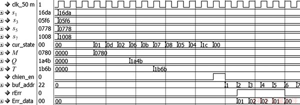
图6 纠错4 bit错的仿真波形
Fig.6 Simulation waveform of correction of 4 bit error
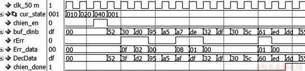
图7 纠错8 bit错的仿真波形
Fig.7 Simulation waveform of correction of 8 bits error
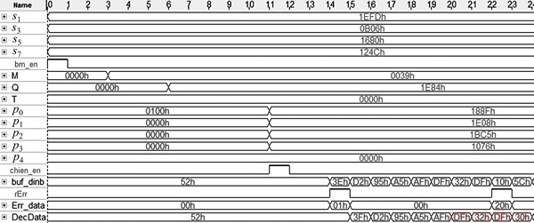
图8 FPGA上实现的译码时序图
Fig.8 Decoding timing diagram acquired from FPGA
5 结论
(1) 提出一种模式可配置的NAND flash纠错系统电路结构,将纠错编码技术与自动重写判断技术相结合,降低了NAND flash的误码率。
(2) 在同等存储介质与工作频率下,该纠错系统电路具有更高的数据吞吐率,即每秒能向NAND flash读写更多的数据。
(3) 对于同等数据处理能力的NAND flash纠错系统电路,本文的实现方法具有更简单的硬件结构,即减小了硬件资源的开销。
(4) 提出的不同NAND flash纠错电路设计方法对降低NADN flash的误码率与读写速度有一定的意义。同时,该纠错系统电路结构独立,方便移植,可用于多种不同的NAND flash应用场合。
参考文献:
[1] Kang M G. DIBL-induced program disturb characteristics in 32-nm NAND flash memory array[J]. IEEE Transactions on Electron Devices, 2011, 58(10): 3626-3629.
[2] LI Longzhen, Lee J H, Kim T H, et al. Design of small-area multi-bit antifuse-type 1 kbit OTP memory[J]. Journal of Central South University of Technology, 2009, 16(3): 467-473.
[3] LI Shu, ZHANG Tong. Improving multi-level NAND flash memory storage reliability using concatenated BCH-TCM coding[J]. IEEE Transactions on Very Large Scale Integration (VLSI) Systems, 2010, 18(10): 1412-1420.
[4] ZHANG Chong, HUANG Mengshu, Okamura L, et al. Error rate decrease through Hamming weight change for nand flash[C]// Proceedings of 2010 10th International Symposium on Communications and Information Technologies. Tokyo, Japan: IEEE, 2010: 1079-1082.
[5] WANG Fangyu, HE Xin, ZHU Wei, et al. Error detection and correction algorithm for RS code based on storage with flash memory[J]. Computer Engineering, 2011, 37(12): 245-247.
[6] Ganesh B, Muralidharan D. Efficient VLSI architecture for low complexity parallel reed solomon decoder[J]. European Journal of Scientific Research, 2012, 73(1): 1079-1082.
[7] LIN Yimin, Yang C H, Hsu C H, et al. A MPCN-based parallel architecture in BCH decoders for NAND flash memory devices[J]. IEEE Transactions on Circuits and Systems Ⅱ: Express Briefs, 2011, 58(10): 682-686.
[8] DONG Guiqiang, XIE Ningde, ZHANG Tong. On the use of soft-decision error-correction codes in NAND flash memory[J]. IEEE Transactions on Circuits and Systems Ⅰ: Regular Papers, 2011, 58(2): 429-439.
[9] XU Yajie, MA Zhi, ZHANG Chunyuan. On classical BCH codes and quantum BCH codes[J]. Journal of Electronics, 2009, 26(1): 64-70.
[10] Kazuaki D, Hideichi S. Quasi-maximum-likelihood-decoding based on hare decision of BCH-code beyond BCH-bound[J]. Science and Engineering Review of Doshisha University, 2003, 44(3): 177-184.
[11] WU Yingquan. New list decoding algorithms for Reed-Solomon and BCH codes[J]. IEEE Transactions on Information Theory, 2008, 54(8): 3611-3630.
[12] Park J I, Lee H. Area-efficient truncated Berlekamp-Massey architecture for reed-solomon decoder[J]. Electronics Letters, 2011, 47(4): 241-243.
[13] Hu T H, Chang M H, Su I J. A modified step-by-step decoding for binary BCH codes[J]. International Journal of Electrical Engineering, 2006, 13(4): 397-404.
[14] 肖潇, 杨路明, 王伟平. 高损耗无线网络中基于网络编码的广播重传策略[J]. 中南大学学报: 自然科学版, 2008, 39(6): 1291-1295.
XIAOXiao,YANGLuming,WANGWeiping. High loss wireless broadcasting retransmission scheme based on network coding[J]. Journal of Central South University: Science and Technology, 2008, 39(6): 1291-1295.
[15] Bellorado J, Kavcic A. Low-complexity soft-decoding algorithms for reed-solomon codes. Part Ⅰ: An algebraic soft-in Hard-O[J]. IEEE Transactions on Information Theory, 2010, 56(3): 945-959.
(编辑 陈灿华)
收稿日期:2012-06-07;修回日期:2012-08-22
基金项目:国家自然科学基金资助项目(61178017)
通信作者:徐富新(1965-),男,湖南邵阳人,副教授,从事光电信息技术和虚拟仪器技术研究;电话:0731-88836313;E-mail: xfx.300@163.com

