沉积温度对硬质合金基体表面硼掺杂金刚石涂层性能的影响
来源期刊:中国有色金属学报(英文版)2018年第4期
论文作者:沈彬 陈苏琳 孙方宏
文章页码:729 - 738
关键词:热丝化学气相沉积;金刚石薄膜;硼掺杂;基体温度;硬质合金
Key words:hot filament chemical vapor deposition; diamond film; boron doping; substrate temperature; tungsten carbide
摘 要:采用热丝化学气相沉积法在硬质合金基体表面沉积一层硼掺杂金刚石(BDD)薄膜,沉积温度为450~850 °C。研究沉积温度对硬质合金基体表面硼掺杂金刚石涂层性能的影响。研究结果表明,硼掺杂明显有助于提高金刚石涂层的生长速率。当沉积温度为650 °C时,BDD薄膜在硬质合金基体表面的生长速率可达到544 nm/h。这可能是由于反应气体的硼原子降低了薄膜生长的激活能(53.1 kJ/mol),从而加快了沉积化学反应速度。此外,拉曼光谱和X射线衍射结果显示,高浓度硼掺杂(750和850 °C)会破坏金刚石的晶格结构,从而使薄膜内缺陷增加。综上,硬质合金基体表面BDD薄膜的优选沉积温度范围为600~700 °C。
Abstract: Boron-doped diamond (BDD) films were deposited on the tungsten carbide substrates at different substrate temperatures ranging from 450 to 850 °C by hot filament chemical vapor deposition (HFCVD) method. The effect of deposition temperature on the properties of the boron-doped diamond films on tungsten carbide substrate was investigated. It is found that boron doping obviously enhances the growth rate of diamond films. A relatively high growth rate of 544 nm/h was obtained for the BDD film deposited on the tungsten carbide at 650 °C. The added boron-containing precursor gas apparently reduced activation energy of film growth to be 53.1 kJ/mol, thus accelerated the rate of deposition chemical reaction. Moreover, Raman and XRD analysis showed that heavy boron doping (750 and 850 °C) deteriorated the diamond crystallinity and produced a high defect density in the BDD films. Overall, 600-700 °C is found to be an optimum substrate temperature range for depositing BDD films on tungsten carbide substrate.
Trans. Nonferrous Met. Soc. China 28(2018) 729-738
Bin SHEN, Su-lin CHEN, Fang-hong SUN
School of Mechanical Engineering, Shanghai Jiao Tong University, Shanghai 200240, China
Received 23 October 2016; accepted 18 July 2017
Abstract: Boron-doped diamond (BDD) films were deposited on the tungsten carbide substrates at different substrate temperatures ranging from 450 to 850 °C by hot filament chemical vapor deposition (HFCVD) method. The effect of deposition temperature on the properties of the boron-doped diamond films on tungsten carbide substrate was investigated. It is found that boron doping obviously enhances the growth rate of diamond films. A relatively high growth rate of 544 nm/h was obtained for the BDD film deposited on the tungsten carbide at 650 °C. The added boron-containing precursor gas apparently reduced activation energy of film growth to be 53.1 kJ/mol, thus accelerated the rate of deposition chemical reaction. Moreover, Raman and XRD analysis showed that heavy boron doping (750 and 850 °C) deteriorated the diamond crystallinity and produced a high defect density in the BDD films. Overall, 600-700 °C is found to be an optimum substrate temperature range for depositing BDD films on tungsten carbide substrate.
Key words: hot filament chemical vapor deposition; diamond film; boron doping; substrate temperature; tungsten carbide
1 Introduction
Chemical vapor deposition (CVD) diamond films have been expected to be widely utilized in a variety of fields due to their outstanding optical, electrical, mechanical, tribological, biomedical and thermal properties [1-3]. For electrical applications, boron doping is usually applied to enhancing the electronic properties of conventional undoped diamond films [4]. The application of boron (B)-doped diamond (BDD) films in other fields has yet attracted extensive interests. It has been reported that BDD films presented lower friction coefficient and wear rate when sliding with Si3N4 ceramic materials, compared with undoped diamond films [5]. While some other studies found that the wear rate of B-doped nano-crystalline diamond (B-NCD) film is much higher than that of undoped film, and it increases linearly with the B-doping level [6,7]. In spite of its controversial tribological properties, BDD film does exhibit enhanced adhesive strength on the tungsten carbide substrate when compared with undoped diamond films by suppressing the graphitization at the interface of substrate and film [8]. As a consequence, a promising improvement on the cutting performance of BDD coated tools is observed in turning high silicon aluminum alloy materials [5,9,10] and milling graphite [8]. However, the high substrate temperature adopted in conventional BDD film deposition process, which is usually above 800 °C, would lead to a deteriorated performance of BDD coated cutting tools. Especially for micro-tools with diameter less than 0.5 mm, the high deposition temperature always promotes the thermal diffusion of cobalt towards the tool surface and thus largely deteriorates the fracture strength of micro-tools, and then causes the early failure of coated micro-tools [11]. Therefore, depositing BDD films at low temperature is expected to be a feasible solution for these issues.
Depositing diamond films at low temperature (lower than 600 °C) is of great scientific and practical significance because it allows the application of diamond films on biosensors, micro-electro-mechanical systems (MEMS), complementary metal oxide semiconductor (CMOS) devices, electrodes and a wide range of substrate materials that are not applicable to the high temperature of ~800 °C [12]. However, for applications of diamond films in mechanical and tribological fields, where the tungsten carbide is the most popular material used to fabricate components and tools, the most promising advantage of depositing low temperature BDD films is its ability of eliminating the thermal residual stress [13,14], as well as inhibiting the thermal diffusion of cobalt towards the substrate surface. Low temperature deposition of undoped diamond films has been investigated extensively on a variety of substrate materials, e.g., silicon [15-17], SiC [18], glass [19], molybdenum [20], plastic [21], steel [22-25] as well as metals [26]. Nevertheless, few studies on the low temperature deposition of BDD films have been reported. To the best of our knowledge, only two studies have been reported on the successful deposition of BDD films at low temperature. Firstly, ZENG et al [17] implemented the deposition of low temperature BDD film using hot filament CVD (HFCVD) method on a silicon substrate with the substrate temperature as low as 460 °C. Most recently, TAYLOR et al [4] successfully deposited a layer of B-NCD over large areas (up to 50 cm×30 cm) at substrate temperatures of 600-650 °C using a novel microwave plasma enhanced linear antenna chemical vapor deposition apparatus (MW-LA-PECVD), in which three different substrate materials, including silicon, quartz, and glass, were adopted. However, low- temperature deposition of BDD films on tungsten carbide substrates has not been reported yet.
In present study, a variety of BDD films were successfully deposited on the tungsten carbide substrates at substrate temperatures ranging from 450 to 850 °C. The HFCVD method was adopted with a high acetone/ hydrogen volume fraction, aiming at enhancing the growth rate of diamond films. The structural morphology, chemical composition, boron concentration, growth rate as well as the activation energy of deposited BDD films were characterized by scanning electron microscopy (SEM), secondary ion mass spectrometry (SIMS), Raman spectroscopy and X-ray diffractometry (XRD). The effects induced by substrate temperature and boron doping on these characteristics, as well as the growth rate of the films were discussed. Finally, an optimum substrate temperature range was identified for effectively depositing BDD film on the tungsten carbide substrate.
2 Experimental
BDD films were deposited on the cobalt cemented tungsten carbide (WC-6%Co) substrate by adopting the HFCVD method. Before each deposition, a two-step pretreatment was applied on the substrate, including a 30 min ultrasonic treatment using Murakami’s reagent and then a 1 min etching process using Caro’s acid, to remove the cobalt element from its surface. The deposition process was carried out in a tailor-made HFCVD apparatus, in which six tantalum filaments (12 cm in length and 0.6 mm in diameter) were dragged straightly by a high-temperature resistant spring and located 10 mm above the substrate surface in a parallel and equidistance manner. They were heated up to 1800- 2200 °C (measured by a two-color pyrometer) during the deposition to dissociate the reactive gas. No DC bias was applied between the filaments and the substrate. A mixture of acetone ((CH3)2CO) and hydrogen with a relatively high volume fraction of acetone/hydrogen (4.6%) was used as the feed gas. Trimethyl borate (B(OCH3)3), which was dissolved into the acetone at a boron/carbon mole fraction of 0.5%, was adopted as the source of boron dopant. The pressure in the reaction chamber was kept at a low level of 1.6 kPa during the initial nucleation period of 30 min with the aim of enhancing the nucleation density; thereafter, it was elevated up to 4 kPa and kept constant during the rest of the film deposition process. During the deposition, the substrate temperature was monitored by a thermocouple inserted into a hole inside the substrate holder and kept it in direct contact with the substrate, and maintained at a specific value by automatically adjusting the power applied to the tantalum filaments according to the measured values. To investigate the influence of the substrate temperature on the BDD film growth, a variety of BDD films were deposited at substrate temperatures ranging from 450 to 850 °C. Furthermore, for each BDD film sample, the corresponding undoped diamond (UDD) samples were also fabricated under the identical growth condition but eliminating the boron source from the acetone gas. Different growth durations of 10, 8, 3, 2.5 and 2.5 h were respectively adopted for the substrate temperatures of 450, 550, 650, 750 and 850 °C in order to obtain measurable film thickness.
For the characterization, scanning electron microscopy (SEM) was adopted to examine the surface and the cross-section morphologies of deposited samples. Secondary ion mass spectrometry (SIMS) was used to measure the boron concentration of deposited BDD films and the relative sensitivity factor (RSF) method was adopted [27]. In this measurement, a referenced BDD film with boron concentration of 1×1018 cm-3 was fabricated using ion implantation method and measured together with deposited BDD films in order to give quantitative estimations of the boron concentration of measured samples. Raman spectroscopy using an excitation wavelength of 532 nm was employed to analyze the atomic bonding state. To provide a deeper analysis of the sp2 phase in the BDD films, UV laser Raman analysis was also performed. X-ray diffractometry (XRD) was used to analyze the surface crystallization of deposited BDD films. The growth rate of a sample was calculated by dividing its thickness by the corresponding deposition duration. The reported thickness of a sample was the average value of ten thickness measurements at different locations on the SEM image of its cross-section morphology.
3 Results and discussion
3.1 Surface morphologies of as-deposited BDD films
The surface and cross-section morphologies of deposited BDD films were examined using SEM, as presented in Fig. 1. At the substrate temperature of 450 °C, the deposited BDD film exhibits ball-like morphology on which nano-sized diamond crystallites coalesce as small and disperse clusters. These clusters are as small as 200-400 nm in diameter and mainly distributed in the valley area around tungsten carbide grains where the binder phase of cobalt has occupied and been etched during the pretreatment process. It is also noted that these clusters do not coalesce as a continuous diamond layer even after a relatively long deposition time (10 h), which indicates that growth rate of BDD film at such a low substrate temperature is extremely low. Comparatively, at substrate temperatures higher than 550 °C, the deposited BDD films exhibit rugged surface covered by well-faceted diamond crystallites. Estimated from the obtained SEM images of their surface morphologies, the grain sizes of these BDD films increase from ~200 to 500 nm (fine-grained) to ~1 μm (micro-crystalline) as the substrate temperature rises from 550 to 850 °C. With regard to the cross-section morphology, BDD films deposited at 750-850 °C exhibit typical columnar structure, while such columnar structured cross-section morphology of the two BDD films deposited at 550-650 °C becomes ambiguous with the smaller grain size of diamond crystallites. At 450 °C, the BDD film does not present obvious film thickness or clear substrate-film interface.
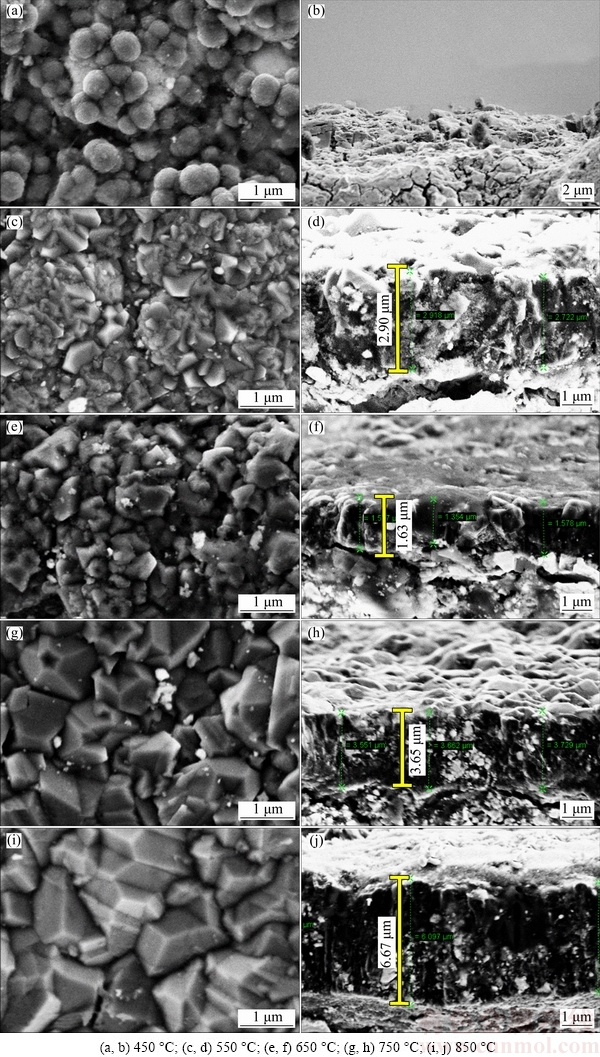
Fig. 1 SEM images of surface morphologies (a, c, e, g, i) and cross-section morphologies (b, d, f, h, j) of BDD films deposited at different temperatures
3.2 Boron concentration
The measured SIMS profiles of the carbon and boron elements for deposited BDD films are depicted in Fig. 2. The boron concentration in BDD film (CBM) is evaluated using the following equation:
CBM=RSF(B/C)(IB/IC) (1)
where RSF(B/C) is the relative sensitivity factor in this system, IB and IC are measured secondary ion intensities of boron and carbon elements, respectively. RSF(B/C) is acquired from the measurement of the referenced BDD film. The measured boron concentrations of deposited BDD films are listed in Table 1. It can be seen that the boron concentration varies from 1.3×10²⁰ to 1.17×1021 cm-3 with increasing substrate temperature, rising nearly one order of magnitude.
3.3 Raman analysis
Raman spectra of deposited BDD films are demonstrated in Fig. 3. It can be observed that the two BDD films, which are deposited at 750 and 850 °C, exhibit the distinctive, asymmetric Fano line shape on their diamond peaks (1332 cm-1), which is an obvious and significant feature of heavily-doped BDD film with boron concentration higher than 1×1021 cm-3 [28]. In contrast, other three BDD films (450-650 °C) show symmetric diamond peaks near 1332 cm-1, indicative of lower boron concentration. Besides the significant Fano effect, the diamond characteristic peak of the two heavily-doped BDD films exhibits obvious downshift of about 12 cm-1 from 1332 cm-1. Comparatively, the diamond peak of BDD film deposited at 650 °C shows only a trivial downshift of about 2 cm-1 and other two BDD films do not exhibit discernable downshift on their diamond peak. Such downshift is associated with the uncertainty of the wavevector owing to the boron incorporating into diamond lattices of the diamond film and becomes significant with increased boron concentration [29].
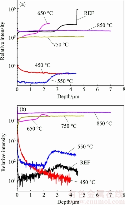
Fig. 2 Measured secondary ion intensities of carbon (a) and boron (b) elements for referenced (REF) sample and BDD films deposited on tungsten carbide substrate at 450-850 °C using SIMS measurement
Table 1 Estimated boron concentrations of BDD films by SIMS measurement
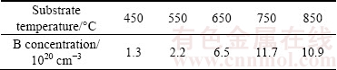
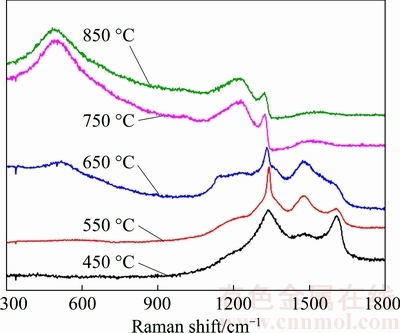
Fig. 3 Raman spectra of BDD films deposited on tungsten carbide substrate at 450-850 °C
Other than the obvious Fano effect and downshift of diamond peak, the two heavily-doped BDD films exhibit distinctive peaks at both 1220 and 500 cm-1, which are characteristics of BDD films with boron concentrations ranging from 2×10²⁰ to 1×1022 cm-3 [17,30]. The peak at 1220 cm-1 represents the combined peak of single optical phonons caused by the incorporation of boron in the diamond lattice and its relative height increases with increasing boron concentration; the 500 cm-1 peak originates from the combination of acoustic phonons in the heavily-doped diamond film [29]. As the boron concentration decreases, these two peaks become broader and weaker, which are apparent in the Raman spectra of BDD films deposited at 550 and 650 °C. The BDD film deposited at 450 °C, due to its relatively low boron concentration of about 1.3×1020 cm-3, only shows a weak characteristic peak at 1217.1 cm-1.
For a BDD film, its Raman peak at 500 cm-1 could be fitted by a Lorentzian component and a Gaussian component and the location wavenumber of the Lorentzian component within the range of 432-500 cm-1 is found to have a one-to-one relationship with its B/C ratio [30]. Adopting this method, the boron concentrations of BDD films deposited at 850, 750, 650 and 550 °C can be estimated to be 7.5×10²⁰, 4.5×10²⁰, 1.1×10²⁰ and 6.7×1019 cm-3, respectively, as derived from the peak fitting shown in Fig. 4. Although this estimation is lower than that derived from SIMS measurements, it still exhibits an increase in boron concentration by one order of magnitude with increasing substrate temperature, which is consistent with that demonstrated by SIMS analysis. Considering the substrate temperature control method adopted in the present study, the increased filament temperature is an important factor because it causes a highly efficient decomposition of reactive gas. In this study, 750 °C might be regarded as the threshold substrate temperature for depositing heavily-doped BDD films on tungsten carbide.
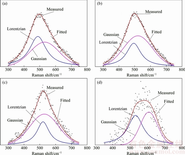
Fig. 4 Deconvolution of peaks at 500 cm-1 of Raman spectra of BDD film deposited at 850 °C (a), 750 °C (b), 650 °C (c) and 550 °C (d) on tungsten carbide substrates
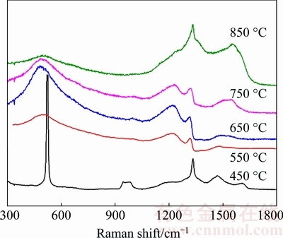
Fig. 5 Raman spectra of BDD films deposited on silicon substrates at 450-850 °C
Such threshold substrate temperature also shows dependence on the substrate material. To verify this, we further deposited BDD films on the silicon substrate, with the identical reactive precursor, at 450-850 °C. The Raman spectra of deposited BDD films are presented in Fig. 5. It can be seen that BDD films deposited at 550 and 650 °C exhibit more distinctive features of heavily boron doping, including the significant Fano effect, a downshift of the diamond peak up to 20 cm-3 as well as strong peaks at both 1220 and 500 cm-1. Their boron concentrations can be estimated to be 2.8×10²⁰ and 8.3×1020 cm-3, respectively. In contrast, the BDD film deposited at 450 °C, similar to the one deposited on the tungsten carbide substrate, only exhibits a weak peak around 1220 cm-1 on its Raman spectrum. This result suggests that the heavily-doped BDD film can be deposited at lower substrate temperature of 550 °C on the silicon substrate.
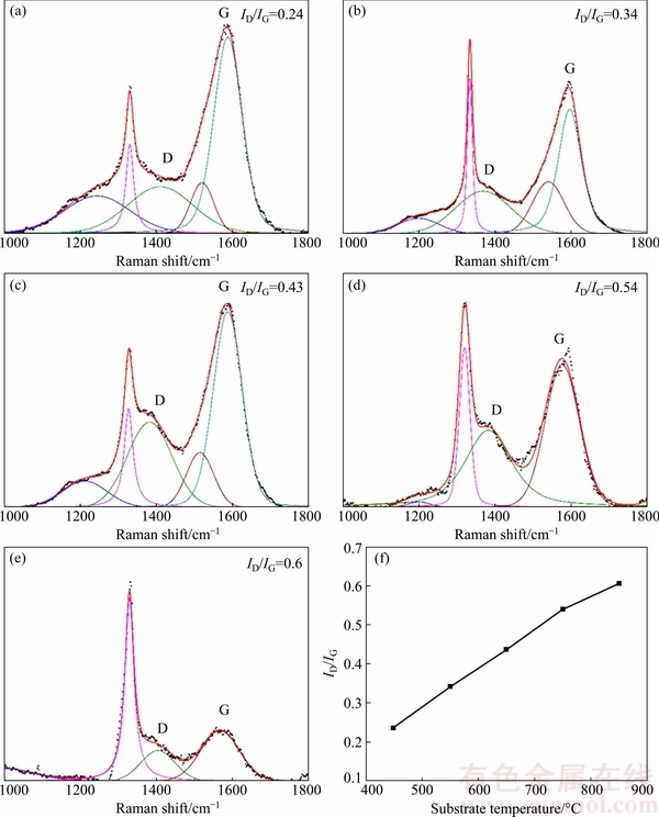
Fig. 6 UV laser Raman spectra for BDD films deposited on tungsten carbide substrates at 450 °C (a), 550 °C (b), 650 °C (c), 750 °C (d), 850 °C (e) and calculated ID/IG ratio as function of substrate temperature (f)
For a diamond film, the D band (~1350 cm-1) and G band (~1580 cm-1) on its Raman spectrum are related with the non-diamond phases due to sp2 sites only. The intensity ratio of them is proportional to the degree of order in the clustered aromatic sp2 phase [31]. To analyze the non-diamond phases present in the deposited BDD films, UV laser Raman spectroscopy is adopted and the deconvolution of bands for the obtained Raman spectra and their ID/IG ratio as a function of substrate temperature, are presented in Fig. 6. It can be observed that all the spectra exhibit obvious diamond characteristic peak (~1332 cm-1), D band (~1350 cm-1) and G band (~1580 cm-1), and the ID/IG ratio presents a nearly linear increasing trend with increased substrate temperature. This indicates increasing amount of non-diamond phases, especially the clustered aromatic sp2 phase, formed in BDD films with elevated substrate temperature.
3.4 XRD analysis
The XRD characterization (Fig. 7) gives consistent results with the UV laser Raman spectroscopic analysis, which provides a further investigation on crystalline structure of deposited BDD films variation with the substrate temperature. All BBD films but the one deposited at 450 °C exhibit the diamond (111) peak at 2θ of ~44° and the diamond (220) peak at 2θ of ~75° on their XRD patterns. The BDD film deposited at 450 °C presents the diamond (220) peak only. Furthermore, the FHWM values of these two peaks decrease with increasing substrate temperature. For the lightly-doped BDD films, this behavior may be attributed to the increasing defect density induced by higher competition with sp2 phase under higher temperatures [32]. For the heavily-doped BDD films, instead, it is due to the incorporation of boron atoms into the diamond lattice. High concentration of boron incorporation destroys the diamond crystallinity and produces a much higher defect density in the BDD films, which induces the broadening of diamond peaks.
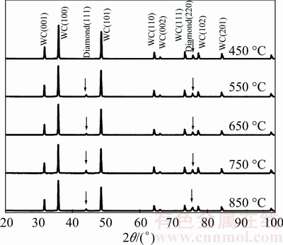
Fig. 7 XRD patterns of BDD films deposited on tungsten carbide substrate at different temperatures
3.5 Growth rate and activation energy
Figure 8 shows the variation of growth rate with the substrate temperature for BDD and UDD films deposited on the tungsten carbide substrate. For all samples, as expected, the growth rate rises with increasing the substrate temperature monotonically and its increasing tendency becomes much sharper as the substrate temperature increases beyond 650 °C. At a specific substrate temperature, the growth rate of the BDD film is always higher than that of the UDD film. Besides, the gap between them rises significantly with increasing substrate temperature. This beneficial effect of the added boron-containing precursor gas on the growth rate of diamond films could be attributed to the favoring effect of the formation of co-adsorbed species (CH2 and BH2) on the CH3 adsorption and H abstraction reactions [4,33]. High substrate temperature promotes these reactions and thus results in the enlarged growth rate gap between the BDD and UDD films.
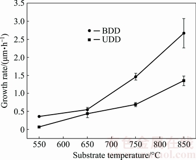
Fig. 8 Dependence of growth rate on substrate temperature for BDD and UDD films deposited on tungsten carbide substrate
It is also noted that relatively high growth rates of BDD films are obtained on the silicon substrate using the same growth atmosphere adopted in the present study. The growth rates of BDD films deposited on the silicon substrate are estimated from the SEM images of their cross-section morphologies, as shown in Fig. 9. The growth rates of ~1.2 μm/h and ~290 nm/h could be achieved for the BDD films deposited at 650 °C (3 h) and 550 °C (8 h), respectively. These are distinctively elevated values compared with the results reported in a recent study, in which a growth rate ranging from 10 to 48 nm/h was obtained for BDD films deposited on glass, quartz as well as silicon substrate with substrate temperatures of 600-650 °C [4]. Even at a low substrate temperature of 450 °C, a much higher growth rate of ~72.2 nm/h can still be obtained on the silicon substrate, compared with the result of ~35 nm/h recently reported in Ref. [17]. For the tungsten carbide substrate, a relatively high growth rate of ~544 nm/h can be obtained for the BDD film at 650 °C, which indicates that the growth chemistry proposed in the present study can lead to high growth rates on both substrates. This can be attributed to the presence of oxygen in the reactive atmosphere, which is originated from both the acetone and the trimethyl borate. Such effect has also been observed in the study by TAYLOR et al [4] who reported that the thickness growth rate of BDD films significantly increases from 10 to 48 nm/h as the volume fraction of CO2/CH4 increases from 0.05% to 0.6 %.
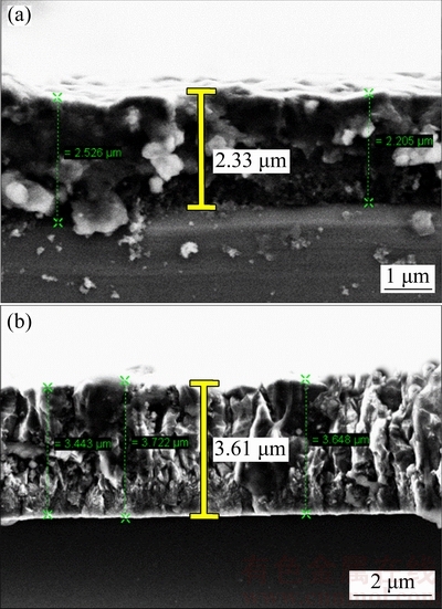
Fig. 9 Cross-section morphologies of BDD films deposited on silicon substrate at 550 °C (8 h) (a) and 650 °C (3 h) (b)
The activation energy (Ea) of diamond film growth reflects the chemical kinetics involving in its growth process and largely depends on the adopted CVD method, growth chemistry, substrate material, substrate temperature and any other factors related with the growth chemical reaction. Figure 10 shows the Arrhenius plot of the BDD and UDD film growth processes as well as the calculated average activation energies, which are about 53.1 and 75.3 kJ/mol, respectively. Regarding a typical HFCVD system adopting the conventional atmosphere consisting of 1% CH4 and 99% H2, an activation energy of ~ 92-100 kJ/mol has been obtained for the substrate of single-crystal (100) p-type silicon wafer with substrate temperatures of 740-930 °C; then it dramatically rises up to 209 kJ/mol as the substrate temperature further reduces to 675-740 °C [34,35]. In the present study, a decreased activation energy of ~75.3 kJ/mol is obtained for the UDD film growth on the tungsten carbide substrate. The substrate material might be a factor causing this decrease as the silicon substrate has been reported to produce higher activation energies than other substrates under the similar growth condition [36]. In this study, the measured activation energies for UDD and BDD film growth on silicon substrates are 80.3 and 75.3 kJ/mol, respectively, both are higher than those on tungsten carbide substrate. Other than the influence of the substrate, the decrease in the activation energy could also be partly attributed to the higher C/H mole ratio in the adopted growth chemistry. It has been reported that adopting a growth atmosphere with elevated CH4/H2 volume ratio of 4%-15% could produce activation energies lower than 41.8 kJ/mol with substrate temperatures of 550-750 °C [32,37]. Besides, the oxygen element in the acetone gas is supposed to be beneficial for the decrease of activation energy. Although this effect has not yet been verified in the HFCVD system, a significantly decreased activation energy of 28 kJ/mol has been obtained in a 50%CO2/50%CH4 (volume fraction) plasma condition of the MPCVD deposition system [38], compared with the typical values of 50 and 37.7 kJ/mol that are generally obtained in a typical 1% CH4/H2 plasma condition for the polycrystalline diamond and NCD films [39].
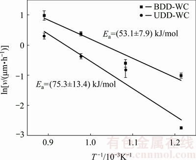
Fig. 10 Arrhenius plots of growth rate (v) for BDD and UDD films on tungsten carbide substrate
For the BDD film, the added boron-containing precursor gas apparently favors the growth rate of chemistry reaction and reduces the activation energy to a relatively low level of 53.1 kJ/mol. Allowing for the faster growth rates presented by the BDD film, compared with the UDD film, increasing the B/C ratio of feed gas might be an effective method enabling the high-rate growth of diamond films at low temperatures, despite only a small fraction of boron atoms in the feed gas could incorporate into diamond lattices. Combining with the boron concentration results, 600-700 °C might be regarded as an optimum substrate temperature range for depositing BDD films on tungsten carbide substrate.
4 Conclusions
1) A variety of boron doped diamond (BDD) films were successfully deposited on the tungsten carbide substrate at substrate temperatures ranging from 450 to 850 °C. With B/C reactive gas with mole fraction of 0.5%, a boron concentration higher than 1×1021 cm-3 could be obtained at 750 °C or above, whereas that of 1×1020 cm-3 could be obtained at 450 °C or above.
2) Increasing amount of non-diamond phases, especially the clustered aromatic sp2 phase, BDD films formed at elevated substrate temperatures. Moreover, boron doping seems to deteriorate the diamond crystallinity and produces a much higher defect density in the BDD films.
3) A relatively high growth rate of ~544 nm/h for BDD film growth could be obtained on the tungsten carbide at 650 °C. This elevated growth rate can be attributed to the presence of oxygen in the reactive atmosphere. Besides, the added boron-containing precursor gas apparently favors the growth rate of chemical reaction and a reduced activation energy of 53.1 kJ/mol. Combining with the boron concentration results, 600-700 °C might be regarded as an optimum substrate temperature range for depositing BDD films on tungsten carbide substrate.
References
[1] AUCIELLO O, SUMANT A V. Status review of the science and technology of ultrananocrystalline diamond (UNCDTM) films and application to multifunctional devices [J]. Diamond and Related Materials, 2010, 19: 699-718.
[2] FENG Jie, XIE You-neng, LI Zhou, WU Xian-zhe, LI Jian-guo, MEI Jun, YU Zhi-ming, WEI Qui-ping. Microscopic mechanical characteristics analysis of ultranano-crystalline diamond films [J]. Transactions of Nonferrous Metals Society of China, 2015, 25: 3291-3296.
[3] WANG Xin-chang, LIN Zi-chao, SHEN Bin, SUN Fang-hong. Effects of deposition parameters on HFCVD diamond films growth on inner hole surfaces of WC-Co substrates [J]. Transactions of Nonferrous Metals Society of China, 2015, 25: 791-802.
[4] TAYLOR A, FEKETE L,  P, MORTET V,
  J. Large area deposition of boron doped nano-crystalline diamond films at low temperatures using microwave plasma enhanced chemical vapour deposition with linear antenna delivery [J]. Diamond and Related Materials, 2014, 47: 27-34.
[5] WANG L, LEI X, SHEN B, SUN F, ZHANG Z. Tribological properties and cutting performance of boron and silicon doped diamond films on Co-cemented tungsten carbide inserts [J]. Diamond and Related Materials, 2013, 33: 54-62.
[6] BUIJNSTERS J G, TSIGKOURAKOS M, HANTSCHEL T, GOMES F O, NUYTTEN T, FAVIA P, BENDER H, ARSTILA K, CELIS J P, VANDERVORST W. Effect of boron doping on the wear behavior of the growth and nucleation surfaces of micro- and nano-crystalline diamond films [J]. ACS Applied Materials & Interfaces, 2016, 8: 26381-26391.
[7] LIANG Q, STANISHEVSKY A, VOHRA Y K. Tribological properties of undoped and boron-doped nanocrystalline diamond films [J]. Thin Solid Films, 2008, 517: 800-804.
[8] LEI X, WANG L, SHEN B, SUN F, ZHANG Z. Effect of boron-doped diamond interlayer on cutting performance of diamond coated micro drills for graphite machining [J]. Materials, 2013, 6: 3128-3138.
[9] WANG L, SHEN B, SUN F, ZHANG Z. Effect of polishing on the friction behaviors and cutting performance of boron-doped diamond films on WC-Co inserts [J]. Surface Review and Letters, 2014, 21: 1450037.
[10] DING W F, XU J H, CHEN Z Z, YANG C Y, SONG C J, FU Y C. Fabrication and performance of porous metal-bonded CBN grinding wheels using alumina bubble particles as pore-forming agents [J]. The International Journal of Advanced Manufacturing Technology, 2013, 67: 1309-1315.
[11] LEI X, SHEN B, CHENG L, SUN F, CHEN M. Influence of pretreatment and deposition parameters on the properties and cutting performance of NCD coated PCB micro drills [J]. International Journal of Refractory Metals and Hard Materials, 2014, 43: 30-41.
[12] LIU Xue-zhang, ZHANG Xiong-wei, YU Zhi-ming. Growth behavior of CVD diamond in microchannels of Cu template [J]. Transactions of Nonferrous Metals Society of China, 2015, 25: 2009-2017.
[13] XIAO X, SHELDON B W, QI Y, KOTHARI A K. Intrinsic stress evolution in nanocrystalline diamond thin films with deposition temperature [J]. Applied Physics Letters, 2008, 92: 131908.
[14] ZHU Y, DING W, XU J, YANG C. An investigation of residual stresses in brazed cubic boron nitride abrasive grains by finite element modelling and Raman spectroscopy [J]. Materials & Design, 2015, 87: 342-351.
[15] RAJANISH N T, LI C. Chemical precursor for the synthesis of diamond films at low temperature [J]. Applied Physics Express, 2010, 3: 045501.
[16] TSUGAWA K, ISHIHARA M, KIM J, KOGA Y, HASEGAWA M. Nucleation enhancement of nanocrystalline diamond growth at low substrate temperatures by adamantane seeding [J]. The Journal of Physical Chemistry C, 2010, 114: 3822-3824.
[17] ZENG H, ARUMUGAM P U, SIDDIQUI S, CARLISLE J A. Low temperature boron doped diamond [J]. Applied Physics Letters, 2013, 102: 223108.
[18] DAS D, JAYASEELAN V, RAMAMURTI R, KUKREJA R S, GUO L, SINGH R N. Low surface temperature synthesis and characterization of diamond thin films [J]. Diamond and Related Materials, 2006, 15: 1336-1349.
[19] LIAO W, WEI D, LIN C. Synthesis of highly transparent ultrananocrystalline diamond films from a low-pressure, low-temperature focused microwave plasma jet [J]. Nanoscale Research Letters, 2012, 7: 82-90.
[20] PIAZZA F,  ROSARIO S A, MORELL G. Synthesis of polycrystalline diamond at low temperature on temperature sensitive materials of industrial interest [J]. International Journal of Refractory Metals and Hard Materials, 2006, 24: 24-31.
[21] TSUGAWA K, ISHIHARA M, KIM J, KOGA Y, HASEGAWA M. Nanocrystalline diamond film growth on plastic substrates at temperatures below 100°C from low-temperature plasma [J]. Physical Review B: Condensed Matter, 2010, 82: 125460.
[22] BUIJNSTERS J G, SHANKAR P, GOPALAKRISHNAN P, VAN ENCKEVORT W J P, SCHERMER J J, RAMAKRISHNAN S S, TER MEULEN J J. Diffusion-modified boride interlayers for chemical vapour deposition of low-residual-stress diamond films on steel substrates [J]. Thin Solid Films, 2003, 426: 85-93.
[23] LIN C R, KUO C T. High adhesion and quality diamond films on steel substrate [J]. Diamond and Related Materials, 1998, 7: 903-907.
[24] SCHWARZ S, ROSIWAL S M, MUSAYEV Y, SINGER R F. High temperature diffusion chromizing as a successful method for CVD-diamond coating of steel―Part II [J]. Diamond and Related Materials, 2003, 12: 701-706.
[25] VELAZQUEZ R, NETO V, UPPIREDDI K, WEINER B, MORELL G. Fabrication of nanodiamond coating on steel [J]. Coatings, 2013, 3: 243-252.
[26] SCHMIDT I, BENNDORF C. Low temperature CVD diamond deposition using halogenated precursors-deposition on low melting materials: Al, Zn and glass [J]. Diamond and Related Materials, 2001, 10: 347-351.
[27] HWANG J H, MASON T O, DRAVID V P. Microanalytical determination of ZnO solidus and liquidus boundaries in the ZnO-Bi2O3 system [J]. Journal of the American Ceramic Society, 1994, 77: 1499-1504.
[28] AGER J W, WALUKIEWICZ W, MCCLUSKEY M, PLANO M A, LANDSTRASS M I. Fano interference of the Raman phonon in heavily boron-doped diamond films grown by chemical vapor deposition [J]. Applied Physics Letters, 1995, 66: 616-618.
[29] ZHANG R J, LEE S T, LAM Y W. Characterization of heavily boron-doped diamond films [J]. Diamond and Related Materials, 1996, 5: 1288-1294.
[30] BERNARD M, DENEUVILLE A, MURET P. Non-destructive determination of the boron concentration of heavily doped metallic diamond thin films from Raman spectroscopy [J]. Diamond and Related Materials, 2004, 13: 282-286.
[31] FERRARI A, ROBERTSON J. Resonant Raman spectroscopy of disordered, amorphous, and diamondlike carbon [J]. Physical Review B: Condensed Matter, 2001, 64: 075414.
[32] BARBOSA D C, ALMEIDA F A, SILVA R F, FERREIRA N G, TRAVA-AIROLDI V J, CORAT E J. Influence of substrate temperature on formation of ultrananocrystalline diamond films deposited by HFCVD argon-rich gas mixture [J]. Diamond and Related Materials, 2009, 18: 1283-1288.
[33] BENNET K, LEE K, KRUCHOWSKI J, CHANG S Y, MARSH M, van ORSOW A, PAEZ A, MANCIU F. Development of conductive boron-doped diamond electrode: A microscopic, spectroscopic, and voltammetric study [J]. Materials, 2013, 6: 5726-5741.
[34] KONDOH E, OHTA T, MITOMO T, OHTSUKA K. Determination of activation energies for diamond growth by an advanced hot filament chemical vapor deposition method [J]. Applied Physics Letters, 1991, 59: 488-490.
[35] KONDOH E, OHTA T, MITOMO T, OHTSUKA K. Surface reaction kinetics of gas-phase diamond growth [J]. Journal of Applied Physics, 1993, 73: 3041-3046.
[36] CHU C J, HAUGE R H, MARGRAVE J L, D’EVELYN M P. Growth kinetics of (100), (110), and (111) homoepitaxial diamond films [J]. Applied Physics Letters, 1992, 61: 1393-1395.
[37] BARBOSA D C, BALDAN M R, TRAVA-AIROLDI V J, CORAT E J. Activation energies for the growth of diamond films and the renucleation of diamond grains during film growth [J]. Journal of Vacuum Science & Technology B, 2014, 32: 031808.
[38] PETHERBRIDGE J R, MAY P W, PEARCE S R J, ROSSER K N, ASHFOLD M N R. Low temperature diamond growth using CO2/CH4 plasmas: Molecular beam mass spectrometry and computer simulation investigations [J]. Journal of Applied Physics, 2001, 89: 1484-1492.
[39] POTOCKY S, KROMKA A, POTMESIL J, REMES Z, POLACKOVA Z, VANECEK M. Growth of nanocrystalline diamond films deposited by microwave plasma CVD system at low substrate temperatures [J]. Physica Status Solidi, 2006, 203: 3011-3015.
沈 彬,陈苏琳,孙方宏
上海交通大学 机械与动力工程学院,上海 200240
摘 要:采用热丝化学气相沉积法在硬质合金基体表面沉积一层硼掺杂金刚石(BDD)薄膜,沉积温度为450~850 °C。研究沉积温度对硬质合金基体表面硼掺杂金刚石涂层性能的影响。研究结果表明,硼掺杂明显有助于提高金刚石涂层的生长速率。当沉积温度为650 °C时,BDD薄膜在硬质合金基体表面的生长速率可达到 544 nm/h。这可能是由于反应气体的硼原子降低了薄膜生长的激活能(53.1 kJ/mol),从而加快了沉积化学反应速度。此外,拉曼光谱和X射线衍射结果显示,高浓度硼掺杂(750和850 °C)会破坏金刚石的晶格结构,从而使薄膜内缺陷增加。综上,硬质合金基体表面BDD薄膜的优选沉积温度范围为600~700 °C。
关键词:热丝化学气相沉积;金刚石薄膜;硼掺杂;基体温度;硬质合金
(Edited by Wei-ping CHEN)
Foundation item: Project (51375011) supported by the National Natural Science Foundation of China; Project (15cxy49) supported by the Shanghai Municipal Education Commission, China; Project (16PJ025) supported by the Shanghai Pujiang Program, China
Corresponding author: Bin SHEN; Tel/Fax: +86-21-34206556; E-mail: binshen@sjtu.edu.cn
DOI: 10.1016/S1003-6326(18)64705-3

