J. Cent. South Univ. Technol. (2009) 16: 0339-0343
DOI: 10.1007/s11771-009-0057-8

Parameter fitting of constitutive model and FEM analysis of
solder joint thermal cycle reliability for lead-free solder Sn-3.5Ag
ZHOU Ping(周 萍), HU Bing-ting(胡炳亭), ZHOU Jie-min(周孑民), YANG Ying(杨 莺)
(School of Energy Science and Engineering, Central South University, Changsha 410083, China)
Abstract: The experimental tests of tensile for lead-free solder Sn-3.5Ag were performed for the general work temperatures range from 11 to 90 ℃ and strain rate range from 5×10⁻⁵ to 2×10⁻² s-1, and its stress―strain curves were compared to those of solder Sn-37Pb. The parameters in Anand model for solder Sn-3.5Ag were fitted based on experimental data and nonlinear fitting method, and its validity was checked by means of experimental data. Furthermore, the Anand model was used in the FEM analysis to evaluate solder joint thermal cycle reliability. The results show that solder Sn-3.5Ag has a better creep resistance than solder Sn-37Pb. The maximum stress is located at the upper right corner of the outmost solder joint from the symmetric center, and thermal fatigue life is predicted to be 3.796×10⁴ cycles under the calculated conditions.
Key words: lead free solder; Sn-3.5Ag alloy; Sn-37Pb alloy; constitutive model; tensile; FEM analysis; thermal cycle reliability
1 Introduction
As the effect of providing both mechanical and electrical connections, solder joints are widely used in electronic packaging. With miniaturization trend of microelectronics, more and more attention has been paid to the thermal-mechanical reliability of solder joints in both the design and failure analysis of electronic devices [1-3]. It is recognized that a major cause of failure in surface mounted electronic devices is that the mismatch of coefficient of thermal expansion (CTE) between components and boards generates thermally induced strains in solder joints by a power and environmental temperature change [4-5]. Therefore, significant efforts have been made to develop a predicting life method of solder connection. Finite element method (FEM) has become a realistic and routine tool in the electronic packaging reliability studies and has been widely used in analyzing the failures of the electronic packages to explore the optimizing design schemes [1-2, 6].
However, in the application of FEM, it is necessary to get a more accurate constitutive model to describe the stress―strain behavior of solder joints. Actually, there have been a lot of experimental and theoretical efforts to develop the constitutive model for varieties of solders, especially for eutectic and near eutectic Sn-Pb solders [4-5, 7-8].
Due to environmental awareness and health hazards involved in using lead in solders, large efforts to develop lead-free soldering have been made in recent years. The most favored lead-free solder alloys recognized by the electronics industry today mainly consist of Sn with small additions of other elements such as silver (Ag), copper (Cu), bismuth (Bi), antimony (Sb) and zinc (Zn) [9-10]. At present, because of low melting temperature, high tensile strength, excellent elongation and mechanical behavior, lead-free solder Sn-3.5Ag has drawn lots of attractions all over the world [11].
In this work, the experimental tests of tensile for solder Sn-3.5Ag were performed at different temperatures in the range of 11 to 90 ℃ and different strain rates in the range of 5×10⁻⁵ to 2×10⁻² s-1, and the material parameters in Anand model were determined according to the experimental data. Furthermore, the model was used in the FEM analysis and thermal cycle reliability of solder joints was evaluated.
2 Experimental
2.1 Experiment procedure
The specimens used in this work were made of Sn-3.5Ag solder alloys, and were prepared by machining from the solder bar to the configuration shown in Fig.1, which had a gauge length of 30 mm, width of 4 mm and thickness of 3 mm. During machining, the surface of the specimen was carefully polished to avoid defections and stress concentration.
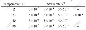
The tensile tests were conducted on a CMT series electronic material testing apparatus. The strain rate was controlled according to the displacement rate of the grip and the specimen gauge length. Temperature was controlled by a GDX series high temperature experiment chamber. During the experiment, the temperature variation was less than (±1) ℃ and temperature gradient in 50 mm gauge length was controlled within 2 ℃. After the specimen was clipped on the grip, it was heated up to the specified temperature, and held on till the temperature was in steady state, and the tensile test started when fracture of the specimen occurred. Considering the fact that the solders with low melting point generally serve at about 50 ℃ in electronic packaging, the testing temperature was determined from 11 to 90 ℃. The detailed test conditions for tensile test are listed in Table 1.
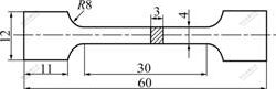
Fig.1 Geometry and dimension of test specimen (Unit: mm)
Table 1 Conditions for tensile test of solder Sn-3.5Ag
2.2 Experimental results and discussion
The experimental stress―strain curves are shown in Fig.2. It can be seen that the saturated stress of solder Sn-3.5Ag is strongly dependent on the test temperature and strain rate. At a constant temperature, the higher the strain rate, the higher the saturated stress. While at a constant strain rate, the higher the temperature, the lower the saturated stress. LANG et al [12] pointed out that, during the deformation, the solders experienced simultaneously strain hardening and dynamic recovery. The two behaviors have contrary influences on the mechanical properties of solders. The former hardens the solders while the latter leads to recovery and softening. Hence, the obtained stress―strain curves represent the combined effects of both behaviors. At higher temperatures, the low strain rate provides a long time for the dynamic recovery, resulting in a decrease in the saturated stress.
2.3 Comparison between solders Sn-3.5Ag and Sn- 37Pb
In order to explore the feasibility of replacing solder Sn-37Pb with solder Sn-3.5Ag, the tensile tests for the traditional solder Sn-37Pb were performed under the same conditions for comparison purposes. Fig.3 shows the experimental stress―strain curves of the two solders at different strain rates or different temperatures. As shown in Fig.3(a), tensile strength of solder Sn-3.5Ag is slightly higher than that of solder Sn-37Pb at 90℃. While from Fig.3(b), it is noted that tensile strength of solder Sn-3.5Ag is lower than that of solder Sn-37Pb at 23 ℃ and 50 ℃. What interests us is, under any testing conditions, stress―strain curves of solder Sn-3.5Ag have better creep resistance. In other words, solder Sn-3.5Ag can last the steady stress for longer time and does not fracture. This excellent performance is significant for solder joint reliability in electronic package.
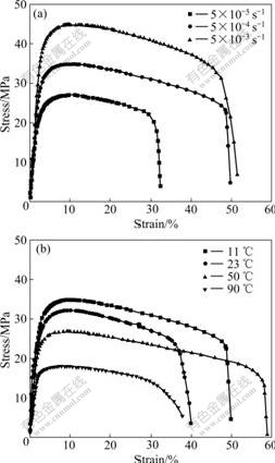
Fig.2 Stress―strain curves of solder Sn-3.5Ag: (a) Constant temperature of 11 ℃; (b) Constant strain rate of 5×10⁻⁴ s-1
3 Anand model
3.1 Parameters fitting for Anand model
Anand model can be written as follows [13]:
 (1)
(1)
where  is the inelastic strain rate, A is the pre- exponential factor, Q is the activation energy, R is universal gas constant, T is the temperature, ξ stands for the material constant, m is the strain rate sensitivity, σ is the equivalent stress for the steady plastic flow, and s is the deformation resistance. If the effect of static recovery for the solder is neglected, the evolution equation for the internal variable s can be represented as and h0 is the hardening/softening constant, a is the strain rate sensitivity of hardening/softening, s* represents a saturation value of internal variable with a given temperature and strain rate,
  is the coefficient, and n is the strain rate sensitivity for the saturation value of deformation resistance.
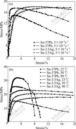
Fig.3 Comparison of tensile properties between solder Sn-3.5Ag and Sn-37Pb: (a) Constant temperature of 90 ℃; (b) Constant strain rate of 5×10⁻⁵ s-1
 (2)
(2)
where
 (3)
(3)
According to the nonlinear curve fitting method suggested by BROWN et al [14] and the above experimental data, the parameters of Anand model for lead-free solder Sn-3.5Ag are fitted and listed in Table 2.
3.2 Model verification
In order to verify the reliability of the parameters of Anand model, stress―strain curve predicted by the above Anand model was compared with that of experi- mental data at 23 ℃ and strain rate of 2×10⁻² s-1 (see Fig.4). The results show that they have a good agreement.
Table 2 Parameters of Anand model for solder Sn-3.5Ag
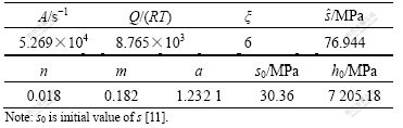
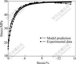
Fig.4 Comparison of stress―strain curves between predicted by Anand model and experimental data
It should be noted that the strain rate used in parameter fitting is in the range from 5×10⁻⁵ to 5×10⁻³ s-1, and strain rate used in model verification is 2×10⁻² s-1 and is different from strain rate range of parameter fitting. Obviously, it can be predicted that if the above Anand model is used to evaluate stress―strain relationship for solder Sn-3.5Ag under the experimental conditions, better results can be got.
4 FEM analysis of solder joint thermal cycle reliability
Miniaturization trend in microelectronics has recently led to the development of ball grid array (BGA) and flip-chip packages [1]. According to the Anand model suggested in this work, FEM analysis was used to evaluate thermal fatigue life for a typical BGA chip, i.e. CBGA chip.
4.1 Physical model
Considering the symmetry of CBGA chip structure, one half of the section was taken as computational zone (see Fig.5). Solder joints were connected to the chip by UBM layer, and joined to substrate through copper pad.
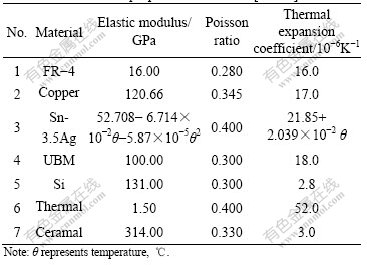
In finite element model, solder material was treated as the viscoplastic material, which can be described by Anand model. Other materials were treated as linear elastic material. Their properties are listed in Table 3.
4.2 Temperature profile loaded
Considering to the temperature range in the tensile experimental test, the range of temperature profile loaded
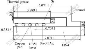
Fig.5 Geometry and dimensions of CBGA chip (Unit: mm)
Table 3 Linear elastic properties of material [15-16]
was determined to be from 9 to 90 ℃. The whole thermal cycle includes ramp-down and ramp-up for 5 min, low temperature and high temperature dwelling for 25 min (see Fig.6). As the reference temperature will not affect stress calculation result [17], 90 ℃ was set as the reference temperature. Furthermore, symmetric boundary condition was loaded to the left edge of the model, and the displacement at the bottom of the substrate was set as 0. Four thermal cycles were loaded to the FE model.
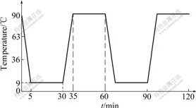
Fig.6 Temperature profile loaded in FEM analysis of CBGA chip
4.3 Computational results and discussion
Equivalent stress contour at the beginning of 9 ℃ of the fourth thermal cycle is shown in Fig.7. The edges of the solder joints are stress concentration spots, and the maximum stress is located at the upper right corner of the outmost solder joint from the symmetric center. As DNP (distance to neutral point) increases, solder joint deformation increases.
In order to study stress and strain responses of the solder joint with maximum stress, average stress and strain values of three nodes located at the upper right of the solder joint vs time are plotted (see Fig.8). Equivalent stress and plastic strain fluctuate as the thermal cycle goes on, which causes the thermal fatigue of solder joint.
From the equivalent stress and plastic strain, hysteresis loops are derived and shown in Fig.9. Every thermal cycle corresponds to a stress―strain cycle, which is a typical thermal fatigue phenomenon. Based on the hysteresis loops, the plastic strain range can be calculated to forecast thermal fatigue life of the solder joint.
Fig.7 Equivalent stress contour at beginning of 9 ℃ of the fourth thermal cycle
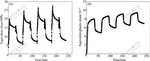
Fig.8 Stress and strain responses of solder joint with maximum stress: (a) Equivalent stress; (b) Equivalent plastic strain
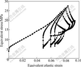
Fig.9 Hysteresis loops of equivalent stress vs equivalent plastic strain
The Coffin-Manson low cycle fatigue life model is as follows:
 (4)
(4)
where Nf is the low cycle fatigue life, m1 is the fatigue ductility exponent, ?εp is the plastic strain range of steady hysteresis loop, and C is the fatigue ductility coefficient.
According to Ref.[16], m1=0.697 8, C=3.921 0. Furthermore, based on the method in Ref.[18], the equivalent plastic strain range calculated from the hysteresis loop is 2.5×10⁻³ and the fatigue life in Eqn.(4) is calculated as Nf=3.796×10⁴ cycles.
5 Conclusions
(1) The experimental tests of tensile for lead-free solder Sn-3.5Ag are carried out at different temperatures and strain rates. Tensile strength of solder Sn-3.5Ag is slightly higher than that of solder Sn-37Pb at higher temperature, such as 90 ℃, but it is lower than that of solder Sn-37Pb at lower temperature, such as 50 ℃. Besides, solder Sn-3.5Ag has a better creep resistance than solder Sn-37Pb.
(2) The parameters in Anand model for lead-free solder Sn-3.5Ag are fitted based on experimental data and nonlinear fitting method, and its validity is checked by experimental data.
(3) Anand model suggested in this work is used in the thermal cycle FEM analysis to calculate stress and strain in the solder joints. The maximum stress is located at the upper right corner of the outmost solder joint from the symmetric center, and thermal fatigue is caused by stress―strain cycle. Based on the stress―strain hysteresis loops and the fatigue life model in reference, thermal fatigue life is predicted to be 3.796×10⁴ cycles.
References
[1] ERINC M, SCHREURS P J G, GEERS M G D. Integrated numerical-experimental analysis of interfacial fatigue fracture in SnAgCu solder joints [J]. International Journal of Solids and Structures, 2007, 44(17): 5680-5694.
[2] SHAM M L, KIM J K, PARK J H. Numerical analysis of plastic encapsulated electronic package reliability: Viscoelastic properties of underfill resin [J]. Computational Materials Science, 2007, 40(1): 81-89.
[3] SHOHJI I, MORI H, ORII Y. Solder joint reliability evaluation of chip scale package using a modified Coffin-Manson equation [J]. Microelectronics Reliability, 2004, 44(2): 269-274.
[4] YANG X J, NASSAR S. Constitutive modeling of time-dependent cyclic straining for solder alloy 63Sn-37Pb [J]. Mechanics of Materials, 2005, 37(7): 801-814.
[5] CHEN Gang, CHEN Xu. Constitutive and damage model for 63Sn37Pb solder under uniaxial and torsional cyclic loading [J]. International Journal of Solids and Structures, 2006, 43(11/12): 3596-3612.
[6] XU L, REINIKAINEN T, REN W, WANG B P, HAN Z X, AGONAFER D. A simulation-based multi-objective design optimization of electronic packages under thermal cycling and bending [J]. Microelectronics Reliability, 2004, 44(12): 1977-1983.
[7] WILDE J, BECKER K, THOBEN M, BLUM W, JUPITZ T, WANG G Z, CHENG Z N. Rate dependent constitutive relations based on Anand model for 92.5Pb5Sn2.5Ag solder [J]. IEEE Transactions on Advanced Packaging, 2000, 23(3): 408-414.
[8] SHI X Q, WANG Z P, ZHOU W, PANG H L J, YANG Q J. A new creep constitutive model for eutectic solder alloy [J]. Journal of Electronic Packaging, 2002, 124(2): 85-90.
[9] ANDERSSON C, LAI Z, LIU J, JIANG H, YU Y. Comparison of isothermal mechanical fatigue properties of lead-free solder joints and bulk solders [J]. Materials Science and Engineering A, 2005, A394(5): 20-27.
[10] HAN Zong-jie, JU Jin-long, XUE Song-bai, FANG Dian-song, WANG Jian-xin, YAO Li-hua. Microstructures of Sn-Ag-Cu lead-free soldered joints with diode-laser soldering [J]. Journal of Central South University: Science and Technology, 2006, 37(2): 229-234. (in Chinese)
[11] CHEN X, CHEN G, SAKANE M. Prediction of stress―strain relationship with an improved Anand constitutive model for lead-free solder Sn-3.5Ag [J]. IEEE Transactions on Components and Packaging Technologies, 2005, 28(1): 111-116.
[12] LANG F Q, TANAKA H, MUNEGATA O, TAGUCHI T, NARITA T. The effect of strain rate and temperature on the tensile properties of Sn-3.5Ag solder [J]. Materials Characterization, 2005, 54(3): 223-229.
[13] ANAND L. Constitutive equations for hot working of metals [J]. International Journal of Plasticity, 1985, 1(3): 213-231.
[14] BROWN S B, KIM K H, ANAND L. An internal variable constitutive model for hot working of metals [J]. International Journal of Plasticity, 1989, 5(2): 95-130.
[15] MASAZUMI A. Characterization of chip scale packaging materials [J]. Microelectronics Reliability, 1999, 39(9): 1365-1377.
[16] CHEN Xiang-yang, ZHOU De-jian. Modeling and reliability analysis of lead-free solder joints of bottom leaded plastic (BLP) package [C]// Proceedings of the 8th IEEE CPMT Conference on High Density Microsystem Design and Packaging and Component Failure Analysis. Shanghai, 2006: 74-80.
[17] PANG J H L, CHONG D Y R, LOW T H. Thermal cycling analysis of flip-chip solder joint reliability [J]. IEEE Transactions on Components and Packaging Technologies, 2001, 24(4): 705-712.
[18] KANCHANOMAI C, MIYASHITA Y, MUTOH Y, MANNAN S L. Influence of frequency on low cycle fatigue behavior of Pb-free solder [J]. Materials Science and Engineering A, 2003, A345(1/2): 90-98.
(Edited by CHEN Wei-ping)
Foundation item: Project(50376076) supported by the National Natural Science Foundation of China
Received date: 2008-09-06; Accepted date: 2008-11-13
Corresponding author: ZHOU Ping, Professor, PhD; Tel: +86-13975804856; E-mail: zhoup@mail.csu.edu.cn

