

![]()
Trans. Nonferrous Met. Soc. China 22(2012) 2504-2511
Langmuir-Blodgett assembly of ultra-large graphene oxide films for transparent electrodes
ZHENG Qing-bin1, 2, SHI Li-fang1, YANG Jun-he1
1. School of Materials Science and Engineering, University of Shanghai for Science and Technology,Shanghai 200093, China;
2. Department of Mechanical Engineering, Hong Kong University of Science and Technology, Hong Kong, China
Received 9 July 2012; accepted 2 August 2012
Abstract:
Monolayer ultra-large graphene oxide (UL-GO) sheets with diameter up to about 100 ��m were synthesized based on a chemical method. Transparent conductive films were produced using the UL-GO sheets that were deposited layer-by-layer on a substrate by the Langmuir-Blodgett (L-B) assembly technique. The films produced from UL-GO sheets with a close-packed flat structure exhibit exceptionally high electrical conductivity and transparency after thermal reduction. A remarkable sheet resistance of 605 ?/sq at 86% transparency is obtained, which outperforms the graphene films grown on a Ni substrate by chemical vapor deposition. The technique used to produce transparent conductive films is facile, inexpensive and tunable for mass production.
Key words:
graphene oxide; Langmuir-Blodgett assembly; transparent electrode; thermal reduction;
1 Introduction
Transparent conductors have been used in a wide variety of optoelectronic and photovoltaic devices, such as touch panels, flat displays, solar cells, optical communication devices and solid-state lighting [1,2]. Graphene, a two-dimensional monolayer of sp2-bonded carbon atoms, has attracted significant interests because of the unique transport properties [3-5]. Due to the high optical transmittance and electrical conductivity, graphene has been considered an alternative material to produce transparent conductive films (TCFs). Compared with traditional electrodes made from indium tin oxide (ITO) or fluorine tin oxide (FTO), graphene films have high mechanical strength, flexibility, chemical stability, and are much cheaper to produce. Many efforts have been directed towards synthesizing graphene sheets that are prepared through mechanical peel-off [6], epitaxial growth [7], or chemical vapor deposition (CVD) [8], as well as transferring them onto transparent substrates using various methods, such as physical contact printing [9] and chemical etching processes [10]. However, these methods are either unsuitable for mass production or require specific substrate materials to grow, significantly limiting their application for large scale production.
Owing to the scalability of production and the convenience in processing, graphene oxide (GO) has now become an important precursor for the fabrication of transparent conductors [11]. These GO dispersions are easy to process to produce transparent conductors on a substrate [12]. TCFs containing GO or chemically- modified GO (rGO) sheets have been deposited via several well-established techniques, including spin- or spray-coating [13,14], transfer printing [15,16], dip coating [17], electrophoretic deposition [18], and Langmuir-Blodgett (L-B) assembly [19-21], followed by further chemical reduction and/or thermal annealing. Among these approaches, the L-B assembly is known to be the only technique that can realize deposition of GO sheets in a layer-by-layer manner and accurate control of the film thickness upon repeated deposition, amenable to optimizing the optoelectrical properties of the final products [22]. Nevertheless, the TCFs made from layer- by-layer deposited GO sheets significantly underperform those made from the CVD-grown graphene in terms of optoelectrical properties because the majority of GO sheets of current use for TCF fabrication is relatively small, in the order of 100 ��m2 at best [17, 23-27]. The improvement in electrical conductivity of the films is severely limited because of the presence of a huge number of intersheet junctions with high contact resistance between the small GO sheets [28]. One effective approach to reduce the sheet resistance of rGO films is through using large area GO sheets so that the number of intersheet tunneling barriers could be decreased.
In this work, we present an efficient and highly reproducible chemical method that involves pre-exfoliation of natural graphite flakes to produce gram quantities of ultra-large graphene oxide (UL-GO) sheets, up to about 100 ��m in lateral size with a yield exceeding 50% by mass. The L-B assembly technique is then used to transfer the UL-GO monolayers onto substrates and produce highly conducting transparent L-B thin films. After thermal reduction, the transparent conductor made from the reduced UL-GO (rUL-GO) sheets shows a sheet resistance of 605 ?/sq at a transmittance of 86% along with a remarkable ��DC/��OP ratio of 3.86. These values are better than those of the graphene films prepared by CVD on a Ni substrate, confirming the beneficial effects of both the ultra-large size of GO and layer-by-layer structure of the film.
2 Experimental
2.1 Preparation of ultra-large graphene oxide sheets
5 g of natural graphite flakes (Asbury Graphite Mills, US) and 150 mL sulfuric acid (H2SO4, 95.5%- 96.5%, General Chemical) were mixed and stirred in a round bottom flask at a speed of 200 r/min. 50 mL of fuming nitric acid (HNO3, Fisher) was then added into the mixture. The mixture was kept at room temperature and stirred for 24 h. 200 mL of de-ionized (DI) water was then poured slowly into the mixture. The resultant mixture was washed with DI water three times, followed by centrifugation and drying at 60 �� for 24 h to obtain graphite intercalation compound (GIC). The dry GIC powder was thermally expanded at 1050 �� for 15 s to obtain expanded graphite (EG) that was used for the production of GO. 1 g of EG and 200 mL of sulfuric acid were mixed and stirred in a three-neck flask. 10 g of KMnO4 was added to the mixture while stirring. The mixture was then stirred at 60 �� for 24 h. The solution was transferred into an ice bath, and 200 mL of de-ionized water and 50 mL of H2O2 were poured slowly into the mixture, realizing colour change of the suspension to light brown. After being stirred for another 30 min, the GO particles were then washed and centrifuged with HCl solution (volume ratio 9:1 of water to HCl) three times, then centrifuged again and washed with de-ionized water until the pH of the solution became 5-6. The GO particles obtained thereby were diluted using DI water (~1 mg/mL) and delaminated by gentle shaking. The GO was then screened to obtain UL-GO and then deposited onto substrate by using L-B technique.
2.2 Preparation of thin film and thermal reduction process
Quartz slides were used as substrates for L-B deposition of UL-GO films. Square slides of 15 mm��15 mm were washed in an acetone bath under ultrasonication to remove any organic contamination, which were immersed in a piranha solution (V(H2SO4):V(H2O2)=7:3) for 1 h, followed by rinsing with distilled water and drying in a vacuum oven for 30 min. For L-B assembly of UL-GO, the L-B trough (KSV Instruments Ltd, MiniMicro LB System) was carefully cleaned with ethanol and then filled with water/methanol mixture. UL-GO solution was slowly spread onto the water surface dropwise using a glass syringe. The solution was spread at a speed of 100 ��L/min up to a total of 5 mL and surface pressure was monitored using a tensiometer attached to a Wilhelmy plate. At the end of the compression, a UL-GO film with faint brown color could be observed. The film was compressed by barriers at a speed of 10 mm/min. The UL-GO monolayer was transferred to a substrate at various points during the compression by vertically dipping the substrate into the trough and slowly pulling it up at a speed of 0.1 mm/min. The substrates were loaded inside a ceramic container with open ends, which was introduced into a furnace (Thermcraft/Eurotherm) with controlled vacuum and gas flow. A vacuum of 133��10-5 Pa was established before heating. The films were heated with a continuous flow of ultra-pure argon, at a rate of 10 ��/min, held at 400 �� for 1.5 h under 133��10-3 Pa, and were allowed to cool to room temperature in argon atmosphere about 20 min. Subsequently, the films were heated to 1100 �� at a rate of 10 ��/min and were held at the same temperature for 0.5 h. After cooling to room temperature, ambient air was admitted to the furnace and the films were recovered to obtain reduced rUL-GO films. The choice of 1100 �� as the graphitization temperature was confirmed effectively [15,16] and the flow of argon gas would eliminate the problem of film loss by reaction with residual oxygen.
2.3 Characterization
A scanning electron microscope (SEM, JSM-6700F, JEOL) was used to characterize the structure and morphology of UL-GO. A tapping-mode atomic force microscope (AFM, scanning probe microscope- nanoscope, digital instruments) was employed to evaluate the surface morphology and the thickness of graphene films. The transparency was characterized using the UV/Vis spectroscopy (Perkin Elmer Lambda 20). The sheet resistance of the films was measured using the four-point probe method (Scientific Equipment & Services). In order to reduce the contact resistance between the probes and the film surface, the four contact points were coated with silver paste. The elemental compositions and the assignments of the carbon peaks were characterized using the X-ray photoelectron spectroscopy (XPS, PHI5600 Physical Electronics), which was equipped with a monochromatic Al K�� X-ray source operated in a residual vacuum of 665��10-9 Pa. Raman spectroscopy (Renishaw MicroRaman/ Photoluminescence System) was used to analyze the effects of post-treatment on the crystal quality of graphene films.
3 Results and discussion
3.1 L-B assembly of UL-GO
The process used to prepare monolayer UL-GO sheets is essentially similar to our previous reports [29,30] and is schematically illustrated in the flow chart in Fig. 1. When the GO sheets were brought together side by side during the L-B assembly, several unique microscopic morphologies were observed through the interactions between the neighboring GO sheets: namely wrinkles, folds and overlaps. These morphological features are undesirable as they reduce the optical transparency of the GO films [31]. Due to the large size ranging from a few tens to about 200 ��m, the UL-GO sheets tend to be softer and more flexible than normal size GO sheets, presenting microscopic morphologies distinct from those observed in S-GO sheets depending on the pressure applied. The corresponding SEM images for the close-packed UL-GO sheets are given in Figs. 2(a) and (b).
The XPS analysis was performed to evaluate the elemental compositions and the functionalities of the UL-GO films. Figure 2(c) shows the general spectrum of the as-prepared UL-GO film with the mole ratio of C to O of 2.42, indicating introduction of many oxygenated groups onto the graphene sheets, which in turn disrupted the sp2-bonded carbon network of graphene. Due to the random distribution, the sp2-hybridized benzene rings are separated by sp3-hybridized rings, thus resulting in insulating GO. As shown in Fig. 2(d), the C 1s signal mainly consisted of five different chemically shifted components that can be deconvoluted into C=C (sp2) in aromatic rings at about 284.8 eV, C��C (sp3) in aromatic rings at about 285.6 eV, C��O (hydroxyl and epoxy) at about 286.6 eV, C=O (carbonyl) at 287.8 eV, and O��C=O (carboxyl) at about 290.3 eV [32,33]. The components of the C��O, C=O and O��C=O groups had 6.7%, 32.5% and 12.5% of the carbon signals, respectively, in the UL-GO film.
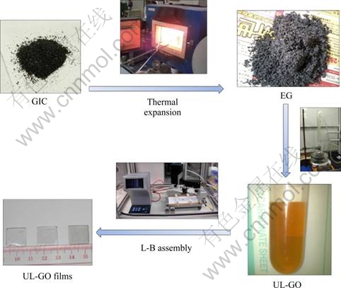
Fig. 1 Preparation flow chart of graphene thin films
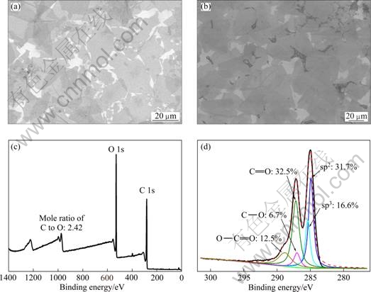
Fig. 2 SEM images of as-prepared UL-GO films consisting of 1 layer (a) and 2 layers (b) of UL-GO deposited on Si substrate, XPS general spectrum (c) and curve fitting of C 1s spectra (d) of as-prepared UL-GO films
3.2 Surface morphology
GO could form a colloidal solution in water due to electrostatic repulsion between the ionized carboxylic and phenol hydroxyl groups that are located on the basal plane of GO sheets with a negative charge [30]. When the second GO layer was deposited on the top of the first layer in our study, these two layers were likely to experience both electrostatic repulsion and van der Waals attraction. Since the GO sheets are brought together on the top of another, their van der Waals potential can be scaled with 1/d2 [19]. The residual ��-conjugated domains can also contribute to the attraction between GO sheets. While these attractive forces dominate and lead to successful layer-by-layer deposition of GO sheets, the GO sheets also experience electrostatic repulsion from both their neighbors and those already deposited, causing wrinkling to occur. In particular, wrinkling becomes serious when depositing a large number of layers, because the substrate is no longer flat due to the presence of GO sheets deposited.
As shown in Fig. 3, the mean surface roughness values of the as-prepared 2 and 10 layers of UL-GO films were 0.82 and 6.85 nm, which were reduced to 0.80 and 5.71 nm respectively, after the thermal treatment. The removal of oxygenated functional groups and graphitization of the films at the high temperature were mainly responsible for the reduction of surface roughness [15,16]. Although the wrinkles and defects cannot be completely removed after thermal treatment, due to the very well aligned structure of the L-B films, the surface roughness was much lower than that of the film produced by other techniques, such as spin or spray coating [13,14], dip coating [17], and transfer printing [15,16,24].
3.3 Opto-electronic properties and surface chemistry
Comparison of optical and electrical properties between rUL-GO films with different number of layers is presented in Fig. 4. A thicker film resulted in a higher degree of light absorption and thus a lower transparency. The sheet resistances of the graphene films measured after the thermal treatment were in the range of 277-605 ?/sq, which are much lower than our previous finding on the graphene films obtained by transfer printing [16]. The thermal treatment removed part of the oxygenated functional groups and helped graphitization of graphene films, which in turn restored the ��-electron system in graphene. Raman spectra of natural graphite and UL-GO obtained before and after thermal treatment are shown in Fig. 5(a). Owing to the presence of isolated double bonds that resonate at frequency higher than that of the G-band of graphite, the G-band peak of UL-GO was up-shifted from 1581 to 1607 cm-1 [34,35]. The corresponding G-band after the thermal reduction (rUL-GO) occurred at 1590 cm-1, which represented the recovery of the hexagonal network of carbon atoms containing defects. G band is Raman active for sp2 hybridized carbon-based material, while D band is activated only if defects participate in the double resonance Raman scattering near K point of Brillouin zone [36]. Hence, the intensity ratio of ID/IG is often used for estimating the sp2 domain size of graphite-based materials. The ID/IG of rUL-GO (1.36) was indeed notably lower than that of UL-GO (1.84), indicating that the thermal reduction process removed the functional groups and recovered the graphitic structure with less defects. Figure 5(b) shows the general spectra of the rUL-GO films, and the mole ratio of C to O was 28.8, indicating the removal of the oxygenated groups. The concentrations of the corresponding functional groups (C��O, C=O and C(=O)��(OH)) after thermal treatments were changed to 8.67%, 3.58% and 3.25%, respectively (Fig. 5(c)). Overall, the above discussion based on the XPS results is consistent with the Raman analysis.
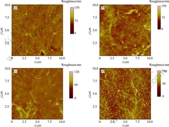
Fig. 3 AFM images of GO films consisting of 2 layers (a, c) and 10 layers (b, d) of monolayer GO sheets before (a, b) and after (c, d) thermal treatment
3.4 Comparison with literature data
The DC to optical conductivity ratio has been proposed to characterize the relative performance in terms of transparency and sheet conductivity differences between transparent conductors with different thicknesses and prepared using different synthesis routes and materials [37]. The relationship between transparency (T) and sheet resistance (Rs) is controlled by the conductivity ratio, ��DC/��Op, using the following equation:
 (1)
(1)
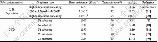
where ��DC is DC conductivity; ��Op is optical conductivity; Z0 (377 ?) is the impedance of free space. A high ��DC/��Op ratio represents a high transmittance and a low sheet resistance, and thus high opto-electrical properties of transparent conductors, and vice versa. Table 1 lists the calculated ��DC/��Op values for transparent conductors made by L-B deposition and CVD method. The ��DC/��Op ratio of the transparent conductors made from UL-GO sheets in this study was 3.86 for rUL-GO consisting of 2 graphene layers, which is comparable with that of graphene films prepared by CVD on a Ni substrate (��DC/��Op of ca. 2-6), demonstrating a great potential for fabricating high performance transparent conductors using UL-GO sheets and highly efficient thermal treatment. In addition, the CVD method usually requires certain substrate materials to be used, and the high cost of these single crystal substrate materials significantly limit the use of CVD method for large scale applications [8]. As described above, films derived from aqueous suspensions of UL-GO through the L-B method can avoid these limitations.
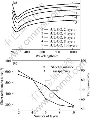
Fig. 4 Comparison of optical and electrical properties of rUL-GO films with different number of layers: (a) Transmittance spectra of rUL-GO films as function of wavelength; (b) Transmittance measured at 550 nm wavelength and sheet resistance

Fig. 5 Raman spectra for natural graphite, UL-GO and rUL-GO (a) and XPS general spectrum (b) and curve fitting of C 1s spectra of rUL-GO (c)
4 Conclusions
1) Transparent conductive films made from graphene or GO sheets have been considered potential replacements for indium tin oxide transparent conductors. Developing methods to produce large size GO sheets with high yield and promote their electrical conductivities is the key to success in such electronic applications. UL-GO sheets up to about 100 ��m in lateral size can be obtained by a combination of thermal expansion and modified chemical methods.
Table 1 Comparison of opto-electrical properties
2) The L-B assembly technique was used to transfer the UL-GO monolayers onto a substrate layer-by-layer. The electrical conductivities of transparent conductors made from closed packed flat UL-GO are improved by thermal reduction.
3) The transparent conductors made from UL-GO sheets show a sheet resistance of 605 ?/sq at a transmittance of 86% along with a remarkable ��DC/��Op ratio of 3.86. Most notably, the opto-electrical properties of our product are comparable with those of the graphene films prepared by CVD on a Ni substrate.
References
[1] WU Z C, CHEN Z H, DU X, LOGAN J M, SIPPEL J, NIKOLOU M, KAMARAS K, REYNOLDS J R, TANNER D B, HEBARD A F, RINZLER A G. Transparent, conductive carbon nanotube films [J]. Science, 2004, 305(5688): 1273-1276.
[2] WANG X, ZHI L J, TSAO N, TOMOVIC Z, LI J L, MULLEN K. Transparent carbon films as electrodes in organic solar cells [J]. Angewandte Chemie International Edition, 2008, 47(16): 2990-2992.
[3] GEIM A K, NOVOSELOV K S. The rise of graphene [J]. Nature Materials, 2007, 6: 183-191.
[4] WANG C, ZHAN L, QIAO W M, LING L C. Preparation of graphene nanosheets through detonation [J]. New Carbon Materials, 2011, 26(1): 21-25.
[5] WANG B, CHANG Y H, ZHI L J. High yield production of graphene and its improved property in detecting heavy metal ions [J]. New Carbon Materials, 2011, 26(1): 31-35.
[6] NOVOSELOV K S, GEIM A K, MOROZOV S V, JIANG D, ZHANG Y, DUBONOS S V, GRIGORIEVA I V, FIRSOV A A. Electric field effect in atomically thin carbon films [J]. Science, 2004, 306(5696): 666-669.
[7] BERGER C, SONG Z, LI X, WU X, BROWN N, NAUD C, MAYOU D, LI T, HASS J, MARCHENKOV A N, CONRAD E H, FIRST P N, de HEER W A. Electronic confinement and coherence in patterned epitaxial graphene [J]. Science, 2006, 312(5777): 1191-1196.
[8] REINA A, JIA X, HO J, NEZICH D, SON H, BULOVIC V, DRESSELHAUS M S, KONG J. Large area, few-layer graphene films on arbitrary substrates by chemical vapor deposition [J]. Nano Letters, 2009, 9(1): 30-35.
[9] LI D, WINDL W, PADTURE N P. Toward site-specific stamping of graphene [J]. Advanced Materials, 2009, 21(12): 1243-1246.
[10] KIM K S, ZHAO Y, JANG H, LEE S Y, KIM J M, KIM K S, AHN J H, KIM P, CHOI J Y, HONG B H. Large-scale pattern growth of graphene films for stretchable transparent electrodes [J]. Nature, 2009, 457(7230): 706-710.
[11] ZHU Y, MURALI S, CAI W, LI X, SUK J W, POTTS J R, RUOFF R S. Graphene and graphene oxide: Synthesis, properties, and applications [J]. Advanced Materials, 2010, 22(35): 3906-3924.
[12] DREYER D R, PARK S, BIELAWSKI C W, RUOFF R S. The chemistry of graphene oxide [J]. Chemical Society Reviews, 2010, 39(1): 228-240.
[13] WATCHAROTONE S, DIKIN D A, STANKOVICH S, PINER R, JUNG I, DOMMETT G H B. EVMENENKO G, WU S E, CHEN S F, LIU C P, NGUYEN S T, RUOFF R S. Graphene-silica composite thin films as transparent conductors [J]. Nano Letters, 2007, 7(7): 1888-1892.
[14] BLAKE P, BRIMICOMBE P D, NAIR R R, BOOTH T J, JIANG D, SCHEDIN F, PONOMARENKO L A, MOROZOV S V, GLEESON H F, HILL E W, GEIM A K, NOVOSELOV K S. Graphene-based liquid crystal device [J]. Nano Letters, 2008, 8(6): 1704-1708.
[15] WANG S J, GENG Y, ZHENG Q B, KIM J K. Fabrication of highly conducting and transparent graphene films [J]. Carbon, 2010, 48(6): 1815-1823.
[16] ZHENG Q B, GUDARZI M M, WANG S J, GENG Y, LI Z G, KIM J K. Improved electrical and optical characteristics of transparent graphene thin films by acid and doping treatments [J]. Carbon, 2011, 49(9): 2905-2916.
[17] WANG X, ZHI L J, MULLEN K. Transparent, conductive graphene electrodes for dyesensitized solar cells [J]. Nano Letters, 2008, 8(1): 323-327.
[18] LEE V, WHITTAKER L, JAYE C, BAROUDI K M, FISCHER D A, BANERJEE S. Large-area chemically modified graphene films: Electrophoretic deposition and characterization by soft X-ray absorption spectroscopy [J]. Chemistry of Materials, 2009, 21(16): 3905-3916.
[19] COTE L J, KIM F, HUANG J X. Langmuir-blodgett assembly of graphite oxide single layers [J]. Journal of the American Chemical Society, 2009, 131(3): 1043-1049.
[20] KIM F, COTE L J, HUANG J X. Graphene oxide: Surface activity and two-dimensional assembly [J]. Advanced Materials, 2010, 22(17): 1954-1958.
[21] LI X L, ZHANG G Y, BAI X D, SUN X M, WANG X R, WANG E G, DAI H J. Highly conducting graphene sheets and langmuir-blodgett films [J]. Nature Nanotechnology, 2008, 3(9): 538-542.
[22] WASSEI J K, KANER R B. Graphene, a promising transparent conductor [J]. Materials Today, 2010, 13(3): 52-59.
[23] BECERRIL H A, MAO J, LIU Z, STOLTENBERG R M, BAO Z, CHEN Y. Evaluation of solution-processed reduced graphene oxide films as transparent conductors [J]. ACS Nano, 2008, 2(3): 463-470.
[24] EDA G, FANCHINI G, CHHOWALLA M. Large-area ultrathin films of reduced graphene oxide as a transparent and flexible electronic material [J]. Nature Nanotechnology, 2008, 3(5): 270-274.
[25] EDA G, LIN Y Y, MILLER S, CHEN C W, SU W F, CHHOWALLA M. Transparent and conducting electrodes for organic electronics from reduced graphene oxide [J]. Applied Physics Letters, 2008, 92(23): 233305.
[26] ZHU Y, CAI W, PINER R D, VELAMAKANNI A, RUOFF R S. Transparent self-assembled films of reduced graphene oxide platelets [J]. Applied Physics Letters, 2009, 95(10): 103104.
[27] KIM Y K, MIN D H. Durable large-area thin films of graphene/ carbon nanotube double layers as a transparent electrode [J]. Langmuir, 2009, 25(19): 11302-11306.
[28] ZHAO J P, PEI S F, REN W C, GAO L B, CHENG H M. Efficient preparation of large-area graphene oxide sheets for transparent conductive films [J]. ACS Nano, 2010, 4(9): 5245-5252.
[29] GENG Y, WANG S J, KIM J K. Preparation of graphite nanoplatelets and graphene sheets [J]. Journal of Colloid and Interface Science, 2009, 336(2): 592-598.
[30] ABOUTALEBI S H, GUDARZI M M, ZHENG Q B, KIM J K. Spontaneous formation of liquid crystal in ultra large graphene oxide dispersions [J]. Advanced Functional Materials, 2011, 21(15): 2978-2988.
[31] COTE L J, KIM J, ZHANG Z, SUN C, HUANG J X. Tunable assembly of graphene oxide surfactant sheets: Wrinkles, overlaps and impacts on thin film properties [J]. Soft Matter, 2010, 6(24): 6096-6101.
[32] MATTEVI C, EDA G, AGNOLI S, MILLER S, MKHOYAN K A, CELIK O, MASTROGIOVANNI D, GRANOZZI G, GARFUNKEL E, CHHOWALLA M. Evolution of electrical, chemical, and structural properties of transparent and conducting chemically derived graphene thin films [J]. Advanced Functional Materials, 2009, 19(16): 2577-2583.
[33] SHIN H J, KIM K K, BENAYAD A, YOON S M, PARK H K, JUNG I S, JIN M H, JEONG H K, KIM J M, CHOI J Y, LEE Y H. Efficient reduction of graphite oxide by sodium borohydride and its effect on electrical conductance [J]. Advanced Functional Materials, 2009, 19(12): 1987-1992.
[34] VOGGU R, DAS B, ROUTT C S, RAO C N. Effects of charge transfer interaction of graphene with electron donor and acceptor molecules examined using Raman spectroscopy and cognate techniques [J]. Journal of Physics: Condensed Matter, 2008, 20(47): 472204.
[35] FERRARI A C, ROBERTSON J. Interpretation of Raman spectra of disordered and amorphous carbon [J]. Physical Review B, 2000, 61(20): 14095-14107.
[36] PIMENTA M A, DRESSELHAUS G, DRESSELHAUS M S, CANCADO L G, JORIO A, SAITO R. Studying disorder in graphite-based systems by Raman spectroscopy [J]. Physical Chemistry Chemical Physics, 2007, 9(11): 1276-1291.
[37] DE S, COLEMAN J N. Are there fundamental limitations on the sheet resistance and transmittance of thin graphene films [J]. ACS Nano, 2010, 4(5): 2713-2720.
[38] WANG Y, CHEN X H, ZHONG Y L, ZHU F R, LOH K P. Large area, continuous, few-layered graphene as anodes in organic photovoltaic devices [J]. Applied Physics Letters, 2009, 95(6): 063302.
[39] LI X S, ZHU Y W, CAI W W, BORYSIAK M, HAN B Y, CHEN D, PINER R D, COLOMBO L, RUOFF R S. Transfer of large-area graphene films for high-performance transparent conductive electrodes [J]. Nano Letters, 2009, 9(12): 4359-4363.
[40] CAI W W, ZHU Y W, LI X S, PINER R D, RUOFF R S. Large area few-layer graphene/graphite films as transparent thin conducting electrodes [J]. Applied Physics Letters, 2009, 95(12): 123115.
Langmuir-Blodgett����װ���Ʊ�����ߴ�����ʯīϩ�����籡Ĥ
֣���1, 2��ʦ����1�����1
1. �Ϻ�������ѧ ���Ͽ�ѧ�빤��ѧԺ���Ϻ� 200093��
2. ��ۿƼ���ѧ ��е����ϵ�����
ժ Ҫ�����û�ѧ�����Ʊ�ֱ��Լ100 ��m�ij���ߴ�����ʯīϩ������Langmuir-Blodgett����װ�������������ڻ�����棬�Ʊ������籡Ĥ���������»�ԭ��ƽ̹���������нṹ��ʯīϩ��Ĥ���иߵ����Լ����ȡ���86%�������£���õı������Ϊ605 ?/sq���˹�����������û�ѧ�����������Ni���������ı�Ĥ���÷��������ײ������ɱ��͡����ڹ�ҵ�����ģ���������ơ�
�ؼ��ʣ�����ʯīϩ��Langmuir-Blodgett����װ�����缫�����»�ԭ
(Edited by LI Xiang-qun)
Foundation item: Project (51102170) supported by the National Natural Science Foundation of China; Project (2010CB234609) supported by the National Basic Research Program of China
Corresponding author: YANG Jun-he; Tel: +86-21-55274065; Fax: +86-21-55270632; E-mail: jhyang@usst.edu.cn
DOI: 10.1016/S1003-6326(11)61492-1
Abstract: Monolayer ultra-large graphene oxide (UL-GO) sheets with diameter up to about 100 ��m were synthesized based on a chemical method. Transparent conductive films were produced using the UL-GO sheets that were deposited layer-by-layer on a substrate by the Langmuir-Blodgett (L-B) assembly technique. The films produced from UL-GO sheets with a close-packed flat structure exhibit exceptionally high electrical conductivity and transparency after thermal reduction. A remarkable sheet resistance of 605 ?/sq at 86% transparency is obtained, which outperforms the graphene films grown on a Ni substrate by chemical vapor deposition. The technique used to produce transparent conductive films is facile, inexpensive and tunable for mass production.
