

Diffusion barrier performance of nanoscale TaNx thin-film
ZHOU Ji-cheng(�ܼ̳�), CHEN Hai-bo(�º���), LI You-zhen(������)
School of Physics Science and Technology, Central South University, Changsha 410083, China
Received 14 September 2006; accepted 8 December 2006
Abstract:
TaNx nanoscale thin-films and Cu/TaNx multilayer structures were deposited on P-type Si(100) substrates by DC reactive magnetron sputtering. The characteristics of TaNx films and thermal stabilities of Cu/TaNx/Si systems annealed at various temperatures were studied by four-point probe(FPP) sheet resistance measurement, atomic force microscopy(AFM), scanning electron microscope-energy dispersive spectrum (SEM-EDS), Alpha-Step IQ Profilers and X-ray diffraction(XRD), respectively. The results show that the surfaces of deposited TaNx thin-films are smooth. With the increasing of N2 partial pressure, the deposition rate and root-mean-square(RMS) decrease, while the content of N and sheet resistance of the TaNx thin-films increase, and the diffusion barrier properties of TaNx thin-films is improved. TaN1.09 can prevent interdiffusion between Cu and Si effectively after annealing up to 650 �� for 60 s. The failure of TaNx is mainly attributed to the formation of Cu3Si on TaN/Si interface, which results from Cu diffusion along the grain boundaries of polycrystalline TaN.
Key words:
reactive magnetron sputtering; TaNx nanoscale thin-film; Cu diffusion barrier; diffusion barrier property;
1 Introduction
One of the urgent research topics for Cu interconnection in ULSI is to find a suitable barrier to prevent Cu diffusion in silicon crystal[1]. The refractory metals and its nitrides have been wildly studied due to their high thermochemical stability and excellent conductivity. Ta-based thin-films, so-called Cu diffusion barrier, are believed to have the brightest application prospect. As a diffusion barrier, Ta has some advantages, such as good adhesion, being immiscible with Cu and low resistivity. But pure Ta thin-film is difficult to be amorphous, so defects (including microcracks, voids and grain boundaries etc) may act as fast diffusion paths and hence decrease the barrier performance. One way to improve the performance is to add N, C or Si into Ta thin-films during the deposition process to change the microstructure[2].
Up to now, Ta and its compounds have been investigated in different aspects. For example, the influence of fabrication methods (sputtering, CVD), microstructure, thickness and annealing ambient of thin-film on diffusion barrier performance[3-4]. However, few researches about this field have been reported in our country. In this study, the influence of N2 partial pressure on the surface morphology, properties of TaNx thin-films, Cu/TaNx multilayer structures was probed. The failure mechanism of TaNx barrier after high temperature annealing was discussed.
2 Experimental
TaNx nanoscale thin-films were deposited onto P-type Si(100) substrates with nominal resistivity of 33-35 ��?cm in N2/Ar ambient by DC reactive magnetron sputtering. The Si wafers were cleaned with RCA (the name from the Radio Corporation of American) method, then were loaded into the vacuum chamber. The base pressure of the system was pumped down to 1.0��10-3 Pa, and the distance between target and substrate is 6 cm. During the TaNx layer deposition, the working pressure was maintained constant at 0.9 Pa, while N2 flow was varied from 5, 7, 15 to 18 cm3/s, respectively, in order to obtain TaNx thin-films with different N contents. The power of Ta target (with the purity of 99.9%, mass fraction) was kept constant at 110 W, while the sputtering time was adjusted from 1 to 3 min, in order to get 50 nm TaNx thin-films at different N2 partial pressures. Then without breaking the vacuum, a 400 nm-thick Cu film was deposited onto some TaNx thin-films to obtain Cu/TaNx/Si multilayer structures. The power of Cu target(with the purity of 99.99%) was 100 W and deposition time was 5 min.
For some samples, the rapid thermal annealing(RTA) was made by tungsten halide lamp at 300-950 �� in N2 ambient with the purity of 99.99%. The ramping rate during temperature increasing process was 100 ��/s. The samples were kept at the set temperature for 60 s and then quickly dropped to room temperature. Alpha-step IQ Profiler was carried out to measure the thickness. The sheet resistance was measured by using a SDY-4D four-point probe. And NT-MDT Solver-P47 AFM was used to measure the root-mean-square(RMS) of surface before and after RTA. Quanta 200 SEM and SEM-EDS were employed to investigate the surface morphology and the component of the thin-films. D/MAX 2550 XRD was used to analyze the crystal structure of TaNx thin-films.
3 Results and discussion
3.1 Effects of N content on properties of TaNx thin- films
The effect of N2 partial pressure on properties of as-deposited TaNx thin-films such as composition, sheet resistance, deposition rate and RMS is summarized in Table 1. In Table 1, the mean deposition rate is equal to the ratio of the thin-films thickness to the deposition time.
Table 1 Effect of N2 partial pressure on properties of as-deposited TaNx thin-films
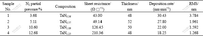
The composition of thin-films in Table 1 was measured by SEM-EDS. Obviously, with the increasing of N2 partial pressure, the content of N in TaNx also increases. The result shows that N atoms in the thin films have two effects. One is reaction with Ta to form compound, and the other is action as impurity in compound. With the increasing of N2 partial pressure during reactive sputtering, TaNx, Ta2N, TaN and Ta3N5 phases will appear sequentially[5-6].
As listed in Table 1, with the N content increasing in TaNx films, the sheet resistance also increases. The sheet resistance is quite sensitive to the N content in the TaNx .thin-films.
Fig.1 shows the effect of annealing temperature on the sheet resistance of the TaNx thin-films. After 500-600 ��, 60 s RTA process, the sheet resistance of the samples decreases obviously. This is mainly due to the grain growth and the defects reduction in the TaNx thin-films. For sample 4, the sheet resistance drops sharply after 600 ��, 60 s RTA. This is mainly due to the ��volatilization�� of N atoms in the thin-film. During the RTA temperature duration of 300-500 ��, the sheet resistance of samples 2-4 abnormally rises. According to the analysis result of SEM-EDS, about 8% O impurity exists in the films, so this abnormal rise of sheet resistance is most probably due to the formation of high resistance oxide from the reaction between O and metallic Ta during RTA process. The similar behavior was observed by ZHANG et al[7], and they considered that the immoderate annealing temperature would increase the dispersion and deviation degree of grain, or there existed a kind of mechanism about grain boundary increasing and transformation at high temperature, then big grain split and mean grain size decreased, so the conductivity of the films became lower.
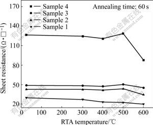
Fig.1 Effect of RTA condition on sheet resistance
From Table 1, it is also found that the deposition rate of TaNx films declines with the increasing of N2 partial pressure. The sputtering yield of N is lower than that of Ar, when keeping working pressure constant. The higher the N2 partial pressure, the less the Ar gas flow. Thus the sputtering yield decreases. Furthermore, the increasing of N2 partial pressure will cause ��target poisoning�� (which means the surface of Ta target becomes into nitrid) and lead to the sputtering mode change from metal to nitride. So the deposition rate declines.
At the same time, with the increasing of N2 partial pressure, the experimental results support that the RMS of TaNx films declines consistently. Lower deposition rate will be helpful to form smoother films and N could refine grains, so TaNx films with high N content have smoother surface. Based on the consideration of application, the surface morphologies of the TaNx thin-films will greatly influence its properties. Lower RMS will be helpful to improve the diffusion barrier performance.
3.2 Effects of N atom content on properties of Cu/ TaNx multilayer structures
Fig.2 shows the sheet resistance change curves as a function of RTA temperature for Cu/TaNx/Si. Since the Cu film is much thicker and has a markedly lower bulk resistivity than TaNx or other reaction products, the measured sheet resistance is dominated by the unreacted Cu films. For Cu/TaN0.36, Cu/TaN0.57, Cu/TaN1.09 and Cu/TaN1.25 samples, the sheet resistance slightly decreases with the RTA temperature increasing up to 550��. This may be due to the reduction of crystal defects and grain growth in the Cu films. However, after RTA at 600, 650, 800 and 850 ��, respectively, the sheet resistance of the samples increases abruptly. This indicates that Cu diffuses into TaNx films and the diffusion barrier is failed. Furthermore, the temperatures, at which the sheet resistances of Cu/TaN0.36, Cu/TaN0.57, Cu/TaN1.09 and Cu/TaN1.25 increase abruptly, are improved gradually, respectively. TaNx thin-films with higher N content could endure higher temperature RTA process. RTA process is inevitable in fabrication of semiconductor device, so TaNx thin-films with higher N content have better diffusion barrier performance.
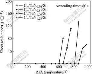
Fig.2 Curves of sheet resistance vs RTA temperature
3.3 Failure mechanism of Cu/TaNx/Si multilayer structures
From the above experimental results, with the increasing of N content, the diffusion barrier property of TaNx films is improved. Generally speaking, the resistivity of Cu diffusion barrier should be less than 1 000 �̦�?cm and the diffusion barrier��s thickness should be less than 100 nm[8]. From our experiment results, in the four TaNx samples, TaN1.09 is the best choice as the diffusion barrier.
Fig.3 shows the XRD patterns of the Cu/TaN1.09/Si samples annealed at various temperatures. For as- deposited sample, there are three Cu diffraction peaks, (111), (200) and (220), respectively. The intensity of Cu (111) is stronger than the other two and the intensity ratio of I(111)/I(200) is 5.1. Generally speaking, when the value of ratio is greater than 3.3, the Cu(111) texture appears in the Cu thin-films[9]. So there is strong Cu(111) texture for all experimental samples. It is well known that strongly oriented Cu(111) film enhances the electromigration stability remarkably just as shown in Ref.[9]. With the RTA temperature increasing up to 750 ��, the intensity of Cu peaks increases, and the peaks become more acuate and tend to move to higher diffraction angle. In addition, Ta2O5 peak appears, which proves the existence of oxygen impurity from the other side. The little amount addition of oxygen is believed to be helpful to improve the diffusion barrier performance [10].
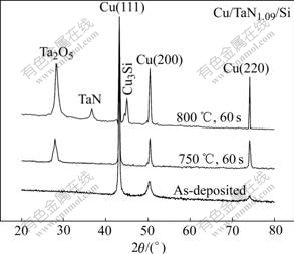
Fig.3 XRD patterns of Cu/TaN1.09/Si multilayer structure
As a contrast, a kind of Cu/Ta/Si multilayer structure is also deposited. Fig.4 shows the XRD patterns of the Cu/Ta/Si samples annealed at various temperatures. For as-deposited sample, Ta has (202) and (002) orientations. But in Fig.3, TaN1.09 remains nano-crystalline/amorphous for as-deposited samples and even if annealed up to 750 �� for 60 s. The deposition parameters for Ta and TaN1.09 are the same, except N2 partial pressure. So it can be concluded that the addition of N delays the TaNx films to crystallize effectively. As shown in Fig.4, the Cu3Si peak appears, when the Cu/Ta/Si samples are annealed at 550 �� for 60 s, which indicates that Ta barrier has failed. Furthermore, the interface reaction product TaSi2 is also detected. By comparing Fig.3 with Fig.4, the addition of N not only improves the diffusion barrier property of TaNx, but also prevents Cu-Si interface reaction, which is usually a common failure mechanism for diffusion barrier.
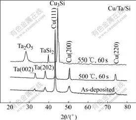
Fig.4 XRD patterns of Cu/Ta/Si multilayer structure
In fact, starting with the columnar-structured polycrystalline thin-films (usually pure refractory metals), there are two ways to reduce their high defect density. The first one is to reduce the amount of grain boundaries, for instance, to deposit giant grains (usually by increasing the adatom mobility), ending up with the fabrication of single crystalline barriers. But to get giant-grained or single crystalline refractory thin-films, the high deposition temperature is required. And this approach does not have any practical application in the semiconductor industry.
The second way is to reduce the defect density by stuffing the existing grain boundaries with light atoms like Si, N and C. This method is to produce nano-crystalline or amorphous-like barrier thin-films by controlling the deposition conditions (gas mixture, ion bombardment, substrate temperature, etc). And this approach is further developed[11].
Fig.5 shows the SEM images of Cu/TaN1.09/Si surface. Fig.5(a) and Fig.5(b) show flat and smooth surface. It means that the multilayer structures can keep stable up to 650 ��. However, after 700 ��, 60 s RTA process, ��black spots�� of different diameters are observed by the naked eyes and many ��bright spots�� appear in the SEM image in Fig.5(c). The origin of the ��spots�� is probably connected with the following two effects. 1) Cu diffuses along some local defects or grain boundaries in the TaNx barrier thin-films into Si substrate and then ��voids�� remain on the Cu surface. In fact, the interdiffusion between Cu and Si occurs simultaneously and some investigations found that the diffusion velocity of Cu through TaNx barrier thin-films is higher than that of Si through barrier. Moreover, the diffusion of Cu will do greater harm than that of Si for Cu interconnection [12-13]. 2) Because of the thermal stress in Cu thin-films, there are Cu grain conglomeration and synergistic effect. And then some hillocks and holes occur and develop.
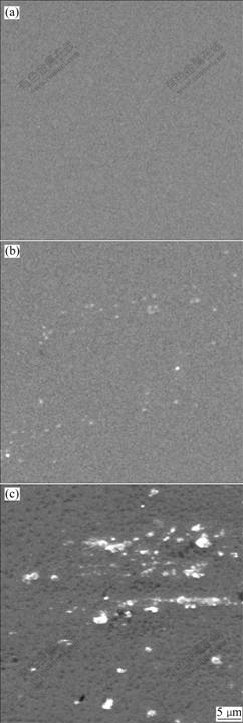
Fig.5 SEM images of Cu/TaN1.09/Si surface: (a) As-deposited; (b) 650 ��, 60 s RTA; (c) 700 ��, 60 s RTA
Fig.6 shows the 3D AFM images of Cu/TaN1.09/Si surface. Before RTA process, the Cu surface is smooth and the grains are uniformly distributed. With the RTA temperature increasing, Cu grain grows and rougher surface is observed. And after higher temperature RTA process, during which the TaN1.09 diffusion barrier is failed, the Cu surface splits into several isolated islands and becomes quite rough.
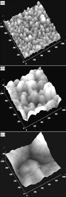
Fig.6 3D AFM images of Cu/TaN1.09/Si surface: (a) As- deposited; (b) 650 ��, 60 s RTA; (c) 700 ��, 60 s RTA
For Cu/TaN1.09/Si multilayer structures, FPP measurement shows that the sheet resistance increases abruptly after 800 ��, 60 s RTA process, and XRD analysis also shows that there are new phase Cu3Si. Obviously, after 700 ��, 60 s RTA process, many ��bright spots�� are observed by SEM. And several other analytical techniques were employed to study the diffusion barrier property and failure mechanism of the thin-film[14]. The failure temperatures are determined as follows: for FPP measurement, the temperature, at which sheet resistance starts to increase abruptly, is defined as failure temperature; for XRD analysis, the failure temperature is that at which TaSi2 or Cu3Si are observed; and for SEM observation, the failure temperature is that at which the ��spots�� appear.
In summary, the failure of TaNx as a Cu diffusion barrier is mainly attributed to the formation of inverse pyramidal Cu3Si[15-16] on TaNx/Si interface, which results from Cu diffusion along the grain boundaries of polycrystalline TaNx.
4 Conclusions
1) The surfaces of as-deposited TaNx thin-films are smooth. With the increasing of N2 partial pressure during reactive sputtering, the N atom content and sheet resistance of the TaNx thin-films increase, the conductivity of the thin-films declines and the deposition rate and RMS decrease.
2) The incorporation of N delays the formation of polycrystalline TaNx and eliminates the interface reaction at TaNx/Si. With the increasing of N content in the TaNx thin-films, the diffusion barrier property of TaNx thin-films improves. Based on the experimental results, TaN1.09 is the best choice for Cu diffusion barrier and it can prevent interdiffusion between Cu and Si effectively, after 650 ��, 60 s RTA process.
3) The failure of TaNx is mainly attributed to the formation of Cu3Si on TaNx/Si interface, which results from Cu diffusion along the grain boundaries of polycrystalline TaNx.
References
[1] WANG Y Y, KANG J F. Development of ULSI interconnect integration technology��Copper interconnect with low k dielectrics [J]. Chinese Journal of Semiconductors, 2002, 23(11): 1121-1134. (in Chinese)
[2] H?BNER R, HECKER M, MATTERN N, HOFFMANN V, WETZIG K, HEUER H, WENZEL C, ENGELMANN H J, GEHRE D, ZSCHECH E. Effect of nitrogen content on the degradation mechanisms of thin Ta-Si-N diffusion barriers for Cu metallization [J]. Thin Solid Films, 2006, 500(1/2): 259-268.
[3] KHIN MAUNG LATT, LEE Y K, LI S, OSIPOWICZ T, SENG H L. The impact of layer thickness of IMP-deposited tantalum nitride films on integrity of Cu/TaN/SiO2/Si multilayer structure [J]. Materials Science and Engineering B, 2001, B84(3): 217-223.
[4] STAVREV M, FISCHER D, WENZEL C, DRESCHER K, MATTERN N. Crystallographic and morphological characterization of reactively sputtered Ta, Ta-N and Ta-N-O thin films [J]. Thin Solid Films, 1997, 307(1/2): 79-88.
[5] YIN K M, LI C, CHEN F R, KAI J J. The effect of oxygen on the interfacial reactions of Cu/TaNx/Si multilayers [J]. Materials Chemistry and Physics, 2001, 71(1): 1-6.
[6] LAURILA T, ZENG K, KIVILAHTI J K, MOLARIUS J, RIEKKINEN T, SUNI I. Tantalum carbide and nitride diffusion barriers for Cu metallization [J]. Microelectronic Engineering, 2002, 60(1/2): 71-80.
[7] ZHANG L W, LU J X, DUAN Q L, WANG H Y, LI R, XIN R M, WANG H J, ZHANG Y X. Technology study of AZO thin films made by magnetron sputtering [J]. Electronic Components and Materials, 2005, 24(8): 46-48.
[8] NICOLET M A. Ternary amorphous metallic thin films as diffusion barriers for Cu metallization [J]. Applied Surface Science, 1995, 91: 269-276.
[9] SONG Z X, XU K W, CHEN H. The effect of nitrogen partial pressure on Zr-Si-N diffusion barrier [J]. Microelectronic Engineering, 2004, 71(1): 28-33.
[10] LEE Y K, KHIN M L, KIM J H, THOMAS O, CHIAM S Y, LEE K. Comparative analysis and study of ionized metal plasma (IMP)-Cu and chemical vapor deposition (CVD)-Cu on diffusion barrier properties of IMP-TaN on SiO2 [J]. Materials Science and Engineering B, 2000, B77: 282-287.
[11] NICOLET M A. Ternary amorphous metallic thin films as diffusion barriers for Cu metallization [J]. Applied Surface Science, 1995, 91(1/4): 269-276.
[12] RHA S K, LEE W J, LEE S Y, HWANG Y S, LEE Y J, KIM D I, KIM D W, CHUN S S, PARK C O. Improved TiN film as a diffusion barrier between copper and silicon [J]. Thin Solid Films, 1998, 320: 134-140.
[13] CHANG C C, JENG J S, CHEN J S. Microstructural and electrical characteristics of reactively sputtered Ta-N thin films [J]. Thin Solid Films, 2002, 413: 46-51.
[14] TSUKIMOTO S, MORIYAMA M, MURAKAMI M. Microstructure of amorphous tantalum nitride thin films [J]. Thin Solid Films, 2004, 460: 222-226.
[15] KUO Y L, HUANG J J, LIN S T, LEE C, LEE W H. Diffusion barrier properties of sputtered TaNx between Cu and Si using TaN as the target [J]. Materials Chemistry and Physics, 2003, 80(3): 690-695.
[16] UEKUBO M, OKU T, NII K, MURAKAMI M, TAKAHIRO K, YAMAGUCHI S, NAKANO T, OHTA T. WNx diffusion barriers between Si and Cu [J]. Thin Solid Films, 1996, 286: 170-175.
Foundation item: Project(60371046) supported by the National Natural Science Foundation of China
Corresponding author: ZHOU Ji-cheng; Tel: +86-731-8836381; E-mail: jicheng@mail.csu.edu.cn
