

Absorption and fluorescence spectra of gallium phosphide(GaP) nanoparticles
YUE Long-yi(������)1, ZHANG Zhao-chun(���״�)1, CHEN Xu(�� ��)2
1. School of Materials Science and Engineering, Shanghai University, Shanghai 200072, China;
2. School of Life Sciences, Shanghai University, Shanghai 200444, China
Received 12 September 2005; accepted 6 March 2006
Abstract:
The optical absorption spectrum ranging from 200 to 800 nm and fluorescence spectra ranging from 300 to 650 nm of GaP nanoparticles at room temperature were reported. From the optical absorption spectrum it is inferred that the GaP nanoparticles exhibit a direct transition of about 410 nm (3.02 eV) and an indirect transition around 480 nm (2.58 eV). In addition, an absorption peak at about 308 nm (4.02 eV) corresponding to the direct transition at higher energy was observed. The absorption peak was attributed to the transition from the spin-orbit-split valence band to the lowest conduction band along the �� direction. By observing the fluorescence of the GaP nanoparticles, it follows that multiple emission bands corresponding to the violet, blue, and yellow light are shown peaking at about 400.4-414.1 nm (3.097-2.994 eV), 450.1-466.8 nm (2.755-2.656 eV), and 582.4 nm (2.129 eV), respectively. The violet and blue light emissions are ascribed to the direct and indirect transitions from conduction band to valence band of the GaP nanoparticles. As to the weak yellow emission, it may be attributed to the radiative recombination from defect centers. The spin-orbit-splitting of the GaP nanoparticles is determined as about 100 meV.
Key words:
absorption; fluorescence; gallium phosphide; nanoparticles;
1 Introduction
In the process of searching for more efficient GaP-based optoelectronic materials, an important way is trying to fabricate materials of lower dimensions in which the motion of electrons and holes is restricted, giving rise to a change in the band gap structure and increase of the energy gap. The Raman spectra of GaP nanowires, synthesized by laser ablation of a powder mixture of GaP and Ga2O3, have been investigated by SHI et al[1]. The down-shift character of the TO and LO modes, partly due to phonon confinement effect in GaP nanowires, was observed. The absorption spectra of GaP nanorods, grown by thermal decomposition of a single- molecular precursor, exhibited strong shoulder (3.46 eV) and shallow tail that were attributed to direct and indirect transition, respectively[2]. The photoluminescence spectrum was 2.79 eV for GaP rods (8��45 nm) corresponding to the direct transition. As can be seen that the GaP nanocrystals show unique spectroscopic features originating from quantum mechanical effects. Typical studies, however, tend to further investigate the band structure of GaP nanomaterials using spectroscopy technique have been poorly explored.
In the previous paper[3], the intrinsic point defects of GaP nanomaterials were investigated by means of electron spin resonance(ESP) technology. An ESR spectrum attributed to the gallium self-interstitial (Gai) was observed with the value g=2.002 8. The spin concen- tration was evaluated as high as 1018 order of magnitude per gram. As we know, when an impurity atom is introduced in a lattice, it produces several types of interactions. The formation of impurity-band is an obvious consequence of increased impurity concentra- tions. Another important effect, i.e., a perturbation of the band by the formation of tails of states extending the bands into the energy gap, can occur[4]. On the other hand, there is still a type of interaction between impurities and the surrounding crystalline: the deformation potential[5]. In the context of GaP nano- particles, Gai atoms evidently induce a deformation potential corresponding to compressional strain, and furthermore, may increase the energy gap.
A direct method for probing the band structure of semiconductor is to measure the absorption spectrum or emission of radiation. One of the main results of the present work is the determination of the direct and indirect energy gap, as well as the E1 energy of the GaP nanoparticles.
2 ExperimentalBy using anhydrous gallium (��) chloride (GaCl3) and sodium phosphide (Na3P) as reactants, GaP nano- particles were grown in dimethylbenzene at 353 K according to the following chemical reaction equation:
GaCl3(anhydrous)+Na3P=GaP(nanoparticles)+3NaCl
The synthesis procedure was reported in Ref.[6].
The X-ray diffraction(XRD) measurement was performed with a single-crystal X-ray diffractometer (D/max-rC) employing Cu K�� radiation from a rotating anode source and a graphite monochromator.
The transmission electron micrograph(TEM) of the GaP nanoparticles was obtained with a JEM-200CX operating at an accelerating voltage of 160 kV.
The absorption measurement was performed at room temperature with a Shimadzu Spectrometer UV-2501Pc (wavelength range between 200 nm and 800 nm). A 3 mm-thick and homogeneous layer of the loose powders was prepared on an aluminum alloy slab mounted within the integrating sphere. Barium sulphate (BaSO4) was chosen as the reference standard. Florescence spectra were obtained at room temperature using a Shimadzu Spectrofluorophotometer RF-540 with wavelengths around 280 and 385 nm, respectively.
3 Results and Discussion3.1 XRD and TEM
Fig.1 shows the powder XRD pattern from as-grown GaP nanoparticles. The application of the Scherrer equation with K= 0.89 to the line broadenings of three diffraction peaks with low angles 2��=28.364?, 47.154? and 55.926?, respectively, generated the average crystallite size of 50.4 nm. Sodium chloride (NaCl), as an impurity, was occluded in the GaP particles.
The TEM image of the GaP nanoparticles is shown

Fig.1 Typical X-ray diffraction pattern of GaP nanoparticles
in Fig.2. It is apparent that the GaP nanoparticles are irregular in shape, but tend to be ellipsoidal rather than spherical. Approximately, the linear dimension of particles was evaluated along only one direction of micrographs, since the random orientation of particles could be assumed. The average size is about 50 nm. Obviously, a mutual aggregation has taken place in the GaP nanoparticles seriously.
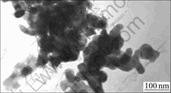
Fig.2 Typical TEM image of GaP nanoparticles
3.2 Absorption spectrum
The absorption spectrum of the GaP nanoparticles is shown in Fig.3. Graphically, the absorption spectrum exhibits a peak at about 308 nm (4.02 eV) and two shoulders at about 480 (2.58 eV) and 410 nm (3.02 eV), respectively. Moreover, a broad tail extends out from about 500 up to 800 nm.
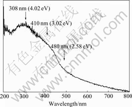
Fig.3 Optical absorption spectrum of GaP nanoparticles at room temperature
As we know, bulk GaP is an indirect semiconductor with an indirect band gap of 559 nm (2.22 eV) and direct band gap of 446 nm (2.78 eV) at room temperature. The shoulder at 410 nm in Fig.3 is attributed to the direct transition, and the steep absorption above 480 nm to the indirect transition in the GaP nanoparticles. It is obvious that both indirect and direct band gaps are blue-shifted from the corresponding bulk value by about 0.34 and 0.24 eV, respectively. By using pseudopotentials Rama Krishna and Friesner have calculated the band gap, band structure and excited-state energies of CdS, GaAs, and GaP semiconductor clusters[7]. Their calculation reveals that the optical spectroscopy of semiconductor clusters is strongly material and crystal structure dependent, and the spectroscopy of small clusters is dramatically different from those of large clusters and bulk. According to their calculation the direct energy gap 3.0 eV for GaP clusters, is corresponding to the mean size of about 3.4 nm. It follows that the GaP nanoparticles with an average grain size around 50 nm seem too ��large�� to show a quantum confinement effect, and should behave as bulk GaP. The discrepancy between theoretical calculation and the present experimental results with regards to grain size can be explained as follows. The blueshift of energy gap in the GaP nanoparticles may be ascribed to that the GaP nanoparticles contain an abundance of microtwins. In our recent work, the Raman scattering analysis of the GaP nanoparticles in which downshift up to about 8 cm-1 was observed for the first-order longitudinal and transverse optical phonon modes in comparison to that of bulk GaP. From theoretical calculation based on a phonon confinement model of Raman scattering from GaP nanowires[8], such a Raman downshift should correspond to an average grain size less than 5 nm. The absorption spectrum and Raman scattering results of the GaP nanoparticles seem to reveal that smaller grains may exist in the GaP nanoparticles in which the quantum confinement effect occurs. Beyond this, the presence of Ga self-interstitials (Gai) in the GaP nanoparticles has significant, if not first order, effect on the blueshifts of indirect and direct bands. It is inferred from the ESR experiments of GaP nanomaterials that the spin concentration is as high as 1018 order of magnitude per gram, indicating that there exists a great deal of Gai in the GaP nanoparticles. LEE has investigated the possible sites of Gai in the lattice of oxygen-doped GaP grown by liquid encapsulated-czochralski(LEC) on the basis of theory prediction by BARAFF and SCHLUTER[9] and by using the optically defected magnetic resonance (ODMR) technology[10]. He proposed that the sites should provide full Td symmetry with cation nearest neighbors. The Gai atoms at Td-symmetric sites evidently induce a deformation potential corresponding to compressional strain, and hence, result in a larger energy gap.
A point which is especially to be noted in connection with GaP nanoparticles is that it seems to be impossible to determine exactly the indirect energy gap only by means of the absorption spectrum. In Fig.3, the steep absorption and shoulder above 480 nm (2.58 eV) is ascribed to the indirect transition between indirect valleys. It is well known that when a transition requires change in both energy and momentum, a two-step process is required because the photon cannot provide a change in momentum; momentum is conserved via a phonon interaction[4]. In the present case, the energy 2.58 eV is not equal to the indirect band gap of the GaP nanoparticles because it is difficult to judge that a phonon is either emitted or absorbed in order to complete the transition from the valence band to the lowest conduct band.
The band peaking at about 308 nm (4.02 eV) is assigned to the E1 structure of the GaP nanoparticles. The E1 structure in the zinc-blende materials is due to transition from the spin-orbit-split valence land to the lowest conduction band along the �� direction[11], i.e., the ��3�C to -��1 transition. It should be noted that because of the undulation of the absorption spectrum in the high-energy region it is very difficult to distinguish the E1 and E1+��1 structures. Consequently, we are not able to determine the value of the ��1 spin-orbit splitting from the absorption spectrum of the GaP nanoparticles. Stokowski and Sell reported that the value of E1 of GaP grown by the Czochralski method was (3.693![]() 0.002) eV at 300 K[11]. By contrast to the value of E1 of GaP single crystal it follows that the E1 energy of the GaP nanoparticles is increased by about 0.3 eV.
0.002) eV at 300 K[11]. By contrast to the value of E1 of GaP single crystal it follows that the E1 energy of the GaP nanoparticles is increased by about 0.3 eV.
It is useful to mention that the absorption tail extends up to 800 nm below the indirect band gap of bulk GaP. It could be caused by Urbach-type band-tailing produced by Gai atoms in the GaP nanoparticles. We note that such subgap absorption below the band gap is also present in GaP quantum dots, which is prepared by mixing GaCl3 and P(SiMe3)3 at room temperature from a GaP precursor and then beating this precursor in a high-boiling solvent[12]. In terms of the ODMR observation by LEE[10], the possible electronic structure of Gai defects based on their lattice sites was considered as the double positive charge state, Gai++. It is also demonstrated that the Gai atoms are ionized. Three stable charge states in energy gap for Gai, at least two defect energy levels, (+/++) and (++/+++), could be considered for defect-defect interactions. As we know, tails of states can result from the perturbation of the band edges by charged impurities. Such a perturbation can produce a local electric field which may be quite large. REDFIELD proposed that the fluctuations of the internal field were responsible for the exponential absorption edge[4].
3.3 Fluorescence
The room temperature fluorescence spectra of the GaP nanoparticles are shown in Fig.4. In order to dispel the effect of overtone and exciting peaks on the fluorescence two wavelengths, 280 nm and 385 nm, were selected as the exciting lasers. It is obvious in Fig.4 that multiple emission bands corresponding to violet, blue, and yellow light are shown peaking at 400.4-414.1 nm (3.097-2.994 eV), 450.1-466.8 nm (2.755-2.656 eV), and 582.4 nm (2.129 eV), respectively.
Based on the fact in Fig.3 that the absorption band peaking at about 410 nm is attributed to the direct transition, the fluorescence emission of 400.4-414.1 nm in Fig.4 is ascribed to the direct band-to-band radiative transition of the GaP nanoparticles. Bulk GaP is an indirect-gap semiconductor, the conduction band has a direct valley of 0.56 eV above the bottom of the lowest valley. In this sense, it seems impossible to observe the direct emission transition. For the GaP nanoparticles, however, the direct transition is observed clearly, indicating that it is possible to excite electrons into both valleys. Although the electrons will rapidly relax to the lowest energy, and in spite of the high self-absorption for the higher photon energy of the direct transition, the direct transition can be detected in the GaP nanoparticles under such adverse conditions only because of the relatively high probability for the direct transition. Beyond this, however, the presence of peak splitting deserves a special mention. In most ��-��group semiconductor compounds the valence band is split by spin-orbit interaction. This interaction lowers one of the three subbands to appreciably lower energies. As a consequence, in the radiative emission a direct transition from the bottom of the conduct band to the top of the valence band can be accompanied by a peak at a slightly higher energy corresponding to a transition to the lower subband. The 400.4-414.1 nm emissions in Fig.4 are due to transitions from ![]() to
to ![]() and from
and from ![]() to
to ![]() , respectively.
, respectively.
The spin-orbit-splitting of the GaP nanoparticles is determined as 103 meV. STOKOWSKI and SELL[12] determined the spin-orbit-splitting as (80![]() 1) meV for bulk GaP at 300 K from the reflectivity and logarithmic derivative of the reflectivity. By using single ribbons of GaP (about 0.35 ��m), DEAN et al[13] carried out high- resolution optical absorption measurements. The direct transition involving hole state in the split-off valence band could be clearly seen at low temperature, and the spin-orbit-splitting was (82
1) meV for bulk GaP at 300 K from the reflectivity and logarithmic derivative of the reflectivity. By using single ribbons of GaP (about 0.35 ��m), DEAN et al[13] carried out high- resolution optical absorption measurements. The direct transition involving hole state in the split-off valence band could be clearly seen at low temperature, and the spin-orbit-splitting was (82![]() 1) meV. CARDONA et al[14] reported the electroreflectance spectra of ��, ��-��, and ��-��group semiconductors. Their measure- ments were performed by electrolyte technique in the 1- to 6- eV photon energy range. A large number of direct interband energy gaps and spin-orbit-splitting were obtained. For GaP, the E0 and E0+��0 transitions were seen at 2.74 and 2.84 eV, and the spin-orbit-splitting was 100 meV. In contrast, the spin-orbit-splitting of the GaP nanoparticles is somewhat higher than those of bulk GaP measured by STOKOWSKI and DEAN, but in agreement with that measured by CARDONA et al.
1) meV. CARDONA et al[14] reported the electroreflectance spectra of ��, ��-��, and ��-��group semiconductors. Their measure- ments were performed by electrolyte technique in the 1- to 6- eV photon energy range. A large number of direct interband energy gaps and spin-orbit-splitting were obtained. For GaP, the E0 and E0+��0 transitions were seen at 2.74 and 2.84 eV, and the spin-orbit-splitting was 100 meV. In contrast, the spin-orbit-splitting of the GaP nanoparticles is somewhat higher than those of bulk GaP measured by STOKOWSKI and DEAN, but in agreement with that measured by CARDONA et al.
The 450.1-466.8 nm (2.755-2.656 eV) emissions in Fig.4 are attributed to the indirect transitions of the GaP nanoparticles. In an indirect-gap semiconductor the radiative transition, like the optical absorption, must be
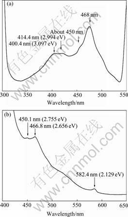
Fig.4 Fluorescence spectra of GaP nanoparticles (Both peaks at 468.7 nm in (a) and peak at 466.8 nm in (b) correspond to transition from X1 to ![]() ): (a) 300-550 nm, peaks at opposite ends correspond to exitation and overtone emissions, respectively; (b) 400-650 nm, peak at left end corresponds to exitation emission
): (a) 300-550 nm, peaks at opposite ends correspond to exitation and overtone emissions, respectively; (b) 400-650 nm, peak at left end corresponds to exitation emission
mediated by an intermediate process which conserves momentum. Phonon emission is the most likely intermediate process. Another momentum-conserving process, phonon absorption, which forms a distinguishable structure in the absorption spectrum, become negligible during emission[4]. Analysis of the results in both Figs.3 and 4 reveals that it seems to be difficult to observe the characteristics of both phonon emission and phonon absorption for the GaP nanoparticles. The transition energies, 2.755 and 2.656 eV, are still not equal to the indirect band gap of the GaP nanoparticles, as explained above. In Fig.4 the indirect transitions in the split-off valence band, X1��![]() and X1��
and X1��![]() , can be seen clearly. The spin-orbit-splitting was evaluated as 99 emV, in good agreement with that from direct transition emissions.
, can be seen clearly. The spin-orbit-splitting was evaluated as 99 emV, in good agreement with that from direct transition emissions.
The photon energy of 582.4 nm (2.129 eV) emission is less than the energy gap of bulk GaP, so it must be related to the transition between a band and an impurity level. The Gai defects might be inclined to be considered. As mentioned above, for Gai at least two defect energy levels (+/++) and (++/+++) could be considered[11]. LEE proposed that as a shallow donor the energy level position of Gai (+/++) should lie above Ec- 0.9 eV. Provided the 582.4 nm emission corresponds to the indirect transition from Gai (+/++) shallow donor to the valence band, the energy level position of Gai (+/++) is evaluated as about 2.656-2.129=0.527 eV if the phonon emission or phonon absorption is disregarded. The spin-orbit-splitting, however, is not observed, because only a single peak at 588.2 nm is present. Provided that the 582.4 nm emission corresponds to the electron transfer from the conduction band to the Gai (++/+++) acceptor, two recombination processes involving Gai (++/+++) are possible. One possibility is a direct electron transfer from ![]() to Gai (++/+++); the other possibility is an indirect electron transfer from X1 to Gai (++/+++). Unfortunately, no experimental or theoretical energy level position of Gai (++/+++) is available, so the recombination process involving Gai (++/+++) could not be determined further in the present experiments.
to Gai (++/+++); the other possibility is an indirect electron transfer from X1 to Gai (++/+++). Unfortunately, no experimental or theoretical energy level position of Gai (++/+++) is available, so the recombination process involving Gai (++/+++) could not be determined further in the present experiments.
4 Conclusions
1) It is found that both the indirect band gap and direct band gap are increased to same extent. The broadening of the energy gap is attributed to the combined effects of quantum confinement and a deformation potential corresponding to compressional strain from gallium self-interstitials.
2) The indirect and direct band-to-band radiative transitions with spin-orbit-splitting of the valence band are observed clearly in the fluorescence spectra of the GaP nanoparticles. From the absorption and fluorescence spectra it can be determined that the direct band gap of GaP nanoparticles with the average grain-size around 50 nm is 2.994 eV, the E1 energy about 4.02 eV, and the spin-orbit-splitting of the valence band about 100 meV. As to the indirect band gap, no exact value is available in the present experiments because of the unambiguousness of phonon-assisting characteristic.
References[1] SHI W S, ZHENG Y F, WANG N, LEE C S, LEE S T. Synthsis and microstructure of galium phosphide nanowires [J]. J Vac Sci Technol B, 2001, 19(4): 1115-1118.
[2] KIM Y H, JUN Y W, JUN B H, LEE S M, CHEON J. Sterically induced shape and crystalline phase control of GaP nanocrystals [J]. J Am Chem Soc, 2002, 124(46): 13656-13657.
[3] ZHANG Zhao-chun, ZOU Lu-jun, CUI De-liang. ESR defection of Ga self-interstitial defects in GaP nano-solids [J]. Mat Sci Eng B, 2004, B111(1): 5-8.
[4] PANKOVE J I. Optical processes in semiconductors [J]. New Jersey: Prentice-Hall, Inc. 1971.
[5] SHOCKLEY W, BARDEEN J. Energy bands and mobilities in monoatomic semiconductors [J]. Phys Rev, 1950, 77(3): 407-408.
[6] CUI De-liang, HAO Xiao-peng, YU Xiao-qiang, SHI Gui-xia, XU Xian-gang, JIANG Min-hua. Synthesis of diphenylene by means of catalytic properties of GaP nano-crystals [J]. Science in China B, 2001, 31(5): 451-455.
[7] RAMA KRISHNA M V, FRIESNER R A. Quantum confinement effects in semiconductor clusters [J]. J Chem Phys, 1991, 95(11): 8309-8322.
[8] XIONG Qi-hua, GUPTA R, ADU K W, DICKEY E C, LIAN G D, THAN D, FRISCHER J E, EKLUND P C. Raman spectroscopy and structure of crystalline gallium phosphide nanowires [J]. J Nanosci Nanotech, 2003, 3(4): 335-339.
[9] BARAFF G A, SCHLUTER M. Electronic structure, total energies, and abundances of the elementary point defects in GaAs [J]. Phys Rev Lett, 1985, 55(12): 1327-1330.
[10] LEE K M. Observation of the Ga self-interstitial defect in GaP [J]. Mat Res Soc Proc, 1988, 104: 449-455.
[11] STOKOWSKI S E, SELL D D. Reflectivity and (dR/dE)/R of GaP between 2.5 and 6.0 eV [J]. Phys Rev B, 1972, 5(4): 1636-1639.
[12] MI?I? O I, SPRANGUE J R, CUETIS C J, JONES K M, MACHOL J L, NOZIK A J, GIESSEN H, FLUEGEL B, MOHS G, PEYGHAMBARIAN N. Synthesis and characterization of InP, GaP, and GaInP2 quantum dots [J]. J Phys Chem, 1995, 99(19): 7754-7759.
[13] DEAN P J, KAMINSKI G, ZETTERSTROM R B. Intrinsic optical absorption of gallium phosphide between 2.33 and 3.12 eV [J]. J Appl Phys, 1967, 38(9): 3551-3556.
[14] CARDONA M, SHAKLEE K L, POLLAK F H. Electroreflectance at a semiconductor-electrolyte interface [J]. Phys Rev, 1967, 154(3): 696-720.
(Edited by LONG Huai-zhong)
Corresponding author: ZHANG Zhao-chun; Tel: +86-21-56331237; E-mail: zhczhang@mail.shu.edu.cn
