

Preparation and characterization of jet-electrodeposited nanocrystalline nickel coatings
PAN Yong(�� ��)1, 2, JIANG Shan(�� ɽ)1, 2, DAI Cui-ying(����Ӣ)1, 2, TANG Tian(�� ��)1, 2,
ZHOU Zhao-feng(����)1, 2, ZHOU Yi-chun(���洺)1, 2
1. Faculty of Materials, Optoelectronic and Physics, Xiangtan University, Xiangtan 411105, China;
2. Key Laboratory of Low Dimensional Materials and Application Technology, Ministry of Education,Xiangtan University, Xiangtan 411105, China
Received 15 July 2007; accepted 10 September 2007
Abstract:
Nanocrystalline nickel coatings were prepared by both direct current(DC) and pulse current(PC) jet-electrodeposition. The influences of current density and jet velocity on the surface morphology, microstructure and preferred orientation of the coatings obtained were investigated by SEM, TEM and XRD. It is found that the current density strongly affects the microstructure of the nickel coating. An increase of the DC current density results in a slight increase of the grain size and preferred orientation progressive evolution (i.e. from (111) to (200)), whereas an increase of the PC current density leads to a certain decrease of the grain size and preferred orientation change (i.e. from (111) to a strong (220)). Moreover, jet velocity shows no significant effect on the grain size and preferred orientation for the nanocrystalline coatings obtained in both DC and PC within the range of jet velocity studied.
Key words:
nanocrystalline nickel; jet-electro deposition; deposition current density; jet velocity;
1 Introduction
Nanocrystalline materials with grain size smaller than 100 nm have attracted considerable interests due to their unique and, in many cases, improved properties over their coarser-grained counterparts[1-3] and exhibited potential extensive applications. In recent years, electrodeposited(ED) nanocrystalline nickel and its alloy coatings have received much attention owing to their potential engineering applications[4-5].
When producing nanostructured coatings, the electrodeposition variables, such as electrolyte composition, temperature, current density, should be chosen properly in order to get massive nucleation of new grains and to reduce growth velocity of the existing grains[4]. According to the electro crystallization theory, the over potential is established by Tafel equation as follows[6]:
��=a+blgj (1)
where a and b are constants, j is the current density,and �� is the over-potential. According to Eqn.(1) the higher the current density, the higher the over-potential. It is known that the grain size of coatings decreases with the increase of current density almost in all pulse current (PC) electrodeposition[7-8].In contrast, the grain size of coatings significantly increases with deposition current density in some direct current(DC) electrodeposition[9].
To better understand the effect of current density on the grain size of the nickel coatings, we developed nickel coating electrodepositing processes using the jet- electrodeposition technique under both DC and PC conditions, and further investigated the influence of deposition parameters such as current density and jet velocity on the microstructure of the nickel coating. Moreover, possible growth mechanisms under both DC and PC conditions were also discussed based on our the experimental results obtained.
2 Experimental
2.1 Experimental apparatus
Fig.1 schematically shows the jet-electroplating apparatus. The jet-plating cell made of Plexiglas is located on the upside of the solution bath. A titanium tube with an exit diameter of 10 mm on the top of the cell acts as an insoluble anode. There is a Plexiglas cathode holder in the middle of the cell. The distance between the tube exit and cathode substrate could be adjusted freely. During the process of electrodeposition the plating solution was forced to go through the tube and flow downward through an air space in the form of an un-submerged circular jet, and then impinged on the cathode substrate. Electrodeposition reaction takes place in the area where the plating solution jet impinged.

Fig.1 Schematic illustration of impinging jet-electroplating setup
In the process of electrodeposition, the applied current density should not exceed a limited value. In general, the limited current density Jl is given by
![]() (2)
(2)
where z is the electronic charge of ion, F is the Faraday constant, D is the diffusion coefficient of metal ion in the plating solution, C0 is the bulk concentration of metal ion in the solution, and �� is the thickness of diffusion layer near the cathode. According to Eqn.(2), the limited current density can be enhanced by thinning the diffusion layer, i.e. reducing the value of ��. As shown in Fig.1, a jet-electroplating system with a special flowing- electrolyte was used to produce a thin diffusion layer and yield a high limited current density. The system has been developed as a kind of high-speed selective electrodeposition technique with high deposition current density and high deposition rate[10].
2.2 Experimental procedures
Nanocrystalline nickel coatings were produced from using the modified Watts bath containing brighteners by the jet-electrodeposition technique under both DC and PC conditions. The compositions and plating conditions for bath A and B are listed in Table 1. Scanning electron microscope(SEM), X-ray diffraction(XRD) and transmission electron microscope(TEM) were used to investigate the surface morphology and the microstructure of the nickel coatings.
Table 1 Bath compositions and plating conditions for Ni deposition from modified Watts-type baths

3 Results and discussion
3.1 Effect of current density on microstructure of DCJED nickel coatings
Nickel coatings were deposited at the current density of 12, 23, 45, 70 and 90 A/dm2 for DC jet- electrodeposited (DCJED) and of 45, 70, 90, 120, 150 and 180 A/dm2 for pulse jet-electrodeposited (PJED), respectively. The pulse on-time (ton) and off-time (toff) for PJED are 0.1 ms and 0.9 ms, respectively. In order to avoid the influence of mass-transport, all samples were prepared using the same plating solution of bath A (see Table 1) and at the identical jet velocity (![]() ) of 5.0 m/s. Fig.2 shows the surface morphologies of the DCJED nickel coatings obtained from bath A at different current densities of 23, 45, 70 and 90 A/dm2, respectively. It is obvious that nickel coatings obtained at current densities of 23 and 45 A/dm2 exhibit similar surface morphologies. A further increase of current density leads to much rougher surface. These are consistent with the results reported in Ref.[9].
) of 5.0 m/s. Fig.2 shows the surface morphologies of the DCJED nickel coatings obtained from bath A at different current densities of 23, 45, 70 and 90 A/dm2, respectively. It is obvious that nickel coatings obtained at current densities of 23 and 45 A/dm2 exhibit similar surface morphologies. A further increase of current density leads to much rougher surface. These are consistent with the results reported in Ref.[9].
Fig.3 shows the influence of current density on the preferred orientation of the nickel coatings. From Fig.3(a), it can be seen that an increase in the current density results in a progressive change of the preferred orientation from (111) at the lowest current density of 12 A/dm2 to (200) at the highest current density of 90 A/dm2 in the DCJEP coatings. An almost random texture was obtained at lower current density of 23 A/dm2., and the intensity ratio of I(200)/I(111) was 0.37, which is well consistent with the corresponding value (0.42) of standard nickel powder reported by EL-SHERIK et al[7]. According to Eqn.(1), a high current density leads to a high over-potential. Therefore, the formation of the strong (200) texture may be attributed to an increase in the cathodic over-potential with the increase of the current density. The formation of the (111) texture in the

Fig.2 SEM images showing influence of current density(J) on surface morphology of DCJED nickel coatings prepared from bath A with constant jet velocity v of 5.0 m/s: (a) J=23 A/dm2; (b) J= 45 A/dm2; (c) J= 70 A/dm2; (d) J=90 A/dm2

Fig.3 XRD patterns showing influence of current density at constant jet velocity v of 5.0 m/s on preferred orientation: (a) DCJED nickel coatings prepared from bath A; (b) PJED nickel coatings with constant ton of 0.1 ms and toff of 0.9 ms
nanocrystalline nickel coatings at the lowest current density of 12 A/dm2 may be caused by the existence of organic additives (i.e. brighteners) in bath A. In general, the effect of the adsorption of organic molecules at low current density is larger than that at high current density[11]. Thus, the (111) preferred orientation was gradually weakened and changed to (200) when the current density was increased.
The average grain sizes of the DCJED nickel coatings shown in Table 2 are the average values calculated from XRD line-broadening of (111) and (200) diffraction peaks. The average grain sizes as a function of current density is plotted in Fig.4. It is seen that the average grain size of the DCJED nickel coatings increases considerably with increasing current density, which is in agreement with the observations reported by BAKONYI et al[9].
Table 2 Average grain size(d) of DCJED nickel coatings determined by XRD line-broadening at each current density


Fig.4 Effect of current density on average grain size of DCJED and PJED nickel coatings at constant jet velocity of 5.0 m/s
3.2 Effect of current density on microstructure of PJED nickel coatings
As shown in Fig.3(b), for the PJED nickel coatings with on-time of 0.1 ms and off-time of 0.9 ms, the current density inalso affects their preferred orientationBecause of the large adsorption effect of organic additives, the PJED nickel coatings prepared at lower current densities of 45 and 70 A/dm2 exhibit the same texture as the nickel coatings obtained by DCJED shown in Fig.3(a), i.e. (111) texture. On the other hand, the preferred orientation of the PJED nickel coatings is gradually changed to (220) rather than (200) when increasing the peak current density, which is caused by high pulse frequency (1 000 Hz) and low duty cycle (1%). Similar phenomenon was also observed by KOLLIAC et al.
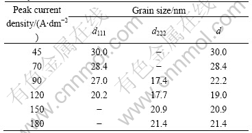
As shown in Fig.3, the X-ray diffraction peaks of (111), (200) or (220) exhibit certain broadening. The average grain sizes of the PJED nickel coatings in Table 3 are the average values calculated from XRD line-broadening of (111) and (220) diffraction peaks. The average grain sizes are plotted in Fig.4 to illustrate the effect of current density on the grain size. In Fig.4 the average grain size of the PJED nickel coatings shows certain decrease with peak current density increasing up to 120 A/dm2, and then slight increase with further increase of current density. The reason is that the Ni2+ ion concentration at the cathode-electrolyte interface in the PJED coatings can recover and keep a constant value before each subsequent pulse starts, as long as the off-time is long enough[12-13]. When the peak current density reaches a certain high value, the pulse off-time in the PJED coatings was insufficient for replenishment of the Ni2+ depleted during a pulse in-time. Consequently, this leads to a drop of the Ni2+ concentration at the cathode-electrolyte interface, which gives rise to a decrease in crystal nucleation rate and hence a slight increase in grain sizes of the deposits.
Table 3 Average grain size(d) of PJED nickel coatings determined by XRD line-broadening at each pulse peak current density
A TEM study was employed for the PJED nickel coatings obtained at the peak current density of 70 A/dm2, and the results are shown in Fig.5. It can be seen clearly from Fig.5(a) that the nickel coating consists of a large number of nanocrystals with an average grain size of approximately 30 nm. A selected-area electron diffraction pattern in Fig.5(b) further confirms the expected ring pattern for such ultra-fine-grain coatings with fcc structure.

Fig.5 TEM bright-field image (a) and diffraction pattern (b) of PJED nickel coating deposited at peak current density Jp=70 A/dm2 onto stainless steel substrate with ton=0.1 ms, toff=0.9 ms at constant jet velocity of 5.0 m/s
3.3 Effect of jet velocity on microstructure of DCJED and PJED nickel coating
The effect of jet velocity on microstructure of the DCJED and PJED nickel coatings was also investigated. The jet velocity(v) in both coatings varied from 1.0 to 5.0 m/s with a constant current density (J or Jp) of 70 A/dm2. The pulse on-time(ton) and off-time(toff) were kept at 0.1 and 0.9 ms for PJED, respectively. The samples were prepared from bath B (see Table 1), which is the same as bath A except for higher concentration of NiSO4. Fig.6 shows the influence of jet velocity on the average grain sizes at the constant current density of 70 A/dm2. It is obvious that the average grain size of the DCJED nickel coatings is progressively decreased with increasing jet velocity, while the average grain size of the PJED coatings is almost unchanged within the variation of the jet velocity from 1.0 to 5.0 m/s. This is because the high-speed flow of plating solution in the DCJED coatings replenished the depleted Ni2+ to some extent, which effectively counteracted the decrease of the crystal nucleation rate and alleviates the grain coarsening. Therefore, the grain size of the DCJED nickel coatings decreases with increasing the jet velocity. In the PJED, however, the replenishment effect induced by the existence of the pulse off-time predominates over the effect due to high-speed flow of plating solution. As a result, the average grain size of the PJED nickel coatings remains almost unchanged with increasing the jet velocity.

Fig.6 Effect of jet velocity on average grain size of DCJED and PJED nickel coatings prepared from bath B at constant current density of 70 A/dm2
Fig.7 shows the influences of jet velocity on the preferred orientation of the coatings produced by the two different methods at a constant current density of 70 A/dm2. It is seen that the preferred orientation in the DCJED coatings is (200) (Fig.7(a)), whereas the preferred orientation is (111) in the PJED coatings (Fig.7(b)). This indicates that the current types can alter

Fig.7 XRD pattern showing influence of jet velocity on preferred orientation: (a) DCJED nickel coatings prepared from bath B at constant J of 70 A/dm2; (b) PJED nickel coatings prepared from bath B at constant Jp of 70 A/dm2 with constant ton of 0.1 ms and toff of 0.9 ms
the preferred orientation even under the same current density condition. In addition, it is found from Fig.6 that the variation of jet velocity shows no obvious effect on the preferred orientation in both cases.
4 Conclusions
1) Nanocrystalline nickel coatings with average grain sizes of 10-50 nm were prepared by direct-current and pulse-current jet-electrodeposition.
2) The average grain size of the nickel coatings significantly increased in DC and initially decreased in PC with increasing deposition current density. With the increase of the jet velocity, the preferred orientation progressively changed from (111) to (200) in DC and from (111) to (220) in PC.
3) An increase in jet velocity led to a certain decrease in average grain size in DC. However, the average grain size remained almost unchanged with increasing jet velocity in PC. In addition, in both DC and PC, the preferred orientation of the Ni coatings remained unaffected within the variation of jet velocity from 1.0 to 5.0 m/s.
References[1] GLEITER H. Nanocrystalline materials [J]. Progr Mater Sci, 1989, 33: 223-228.
[2] SUN C Q. Size dependence of nanostructures: Impact of bond order deficiency [J]. Prog Solid State Chem, 2007, 35: 1-159.
[3] REN X Y. Developing status of nanocoaters and coating technology [J]. Nonferrous Metals, 2004, 56(3): 31-34.
[4] ERB U. Electrodeposited nanocrystals: Synthesis, properties and industrial applications [J]. Nanostruct Mater, 1995, 6(5/8): 533-538.
[5] LI W, DAI M J. Application and manufacturing methods of nanometer coatings [J]. Corrosion & Protection, 2003, 24(5): 197-199.
[6] CHOO R T C, TOGURI J M, EL-SHERIK A M. Mass transfer and electrocrystallization analyses of nanocrystalline nickel production by pulse plating [J]. J Appl Electrochim,1995, 25: 384-389.
[7] EL-SHERIK A M, ERB U, PAGE J. Microstructural evolution in pulse plated nickel electrodeposits [J]. Surf Coat Technol, 1997, 88(1/3): 70-78.
[8] QU N S, ZHU D, CHAN K C. Pulse electrodeposition of nanocrystalline nickel using ultra narrow pulse width and high peak current density [J]. Surf Coat Technol, 2003, 168(2/3): 123-128.
[9] BAKONYI I, TOTH�CKADAR E, POGANY L, CZIRAKI A. Giant magnetoresistance in self-supporting electrodeposited Ni & unknown, Cu/Cu multilayers [J]. J Magnetism and Magnetic Materials, 1996, 156(1/3): 347-349.
[10] ZIMMERMAN A F, PALUMBO G, AUST K T, ERB U. Pulse electrodeposition of Ni-SiC nanocomposite [J]. Materials Letter, 2002, 52(1/2): 85-90.
[11] CZERWINSKI F, PALUMBO G, SZPUNAR J A. Textures of oxide films grown on nickel electrodeposits [J]. Scripta Mater, 1998, 39: 1359-1364.
[12] EL-SHERIK A M, ERB U. Synthesis of bulk nanocrystalline nickel by pulsed electrodeposition [J]. J Mater Sci, 1995, 20(1/2): 177-186.
[13] HIBBARD G D, AUST K T, ERB U. The effect of starting nanostructure on the thermal stability of electrodeposited nanocrystalline Co [J]. Acta Materialia, 2006, 54(9): 2501-2510.
Foundation item: Project(2005AA01210) supported by the Hi-tech Research and Development Program of China; Project(10525211) supported by Fund for Prominent Young Scholars from the Organization of NNSF of China; Project(06C840) supported by Scientific Research Fund of Hunan Provincial Education Department, China
Corresponding author: ZHOU Yi-chun; Tel/Fax: +86-732-8293586; E-mail: zhouyc@xtu.edu.cn
