
Trans. Nonferrous Met. Soc. China 23(2013) 2962-2970
Si-doped diamond films prepared by chemical vapour deposition
Yu-xiao CUI1, Jian-guo ZHANG1, Fang-hong SUN1,2, Zhi-ming ZHANG1,2
1. School of Mechanical Engineering, Shanghai Jiao Tong University, Shanghai 200240, China;
2. Suzhou Jiaozuan Superhard Nanocoatings Co., Ltd., Suzhou 215000, China
Received 12 September 2012; accepted 7 January 2013
Abstract:
The effects of Si doping on morphology, components and structure characteristics of CVD diamond films were studied. Si-doped CVD diamond films were deposited on Si substrate by adding tetraethoxysilane (TEOS) into acetone as source of reactant gas. The morphology and microstructure of diamond films were characterized by scanning electron microcopy (SEM). The crystalline quality of diamond films was studied by Raman spectroscopy and X-ray diffractometry (XRD). The surface roughness of the films was evaluated with surface profilometer. The results suggest that Si doping tends to reduce the crystallite size, enhance grain refinement and inhibit the appearance of (111) facets. Raman spectra indicate that Si doping can enhance the formation of sp2 phase in diamond films. Moreover, Raman signal of SiC was detected, which suggests the existence of Si in the diamond films. Smooth fine-grained diamond (SFGD) film was synthesized at Si to C ratio of 1%.
Key words:
Si doping; hot filament chemical vapor deposition (HFCVD); diamond films;
1 Introduction
Diamond films grown by hot filament chemical vapor deposition (HFCVD) are widely used today because of their attractive features as new functional materials. In many applications, excellent properties of diamond such as extreme hardness, wear resistance, good thermal conductivity and low thermal expansion coefficient are expected to bring significant advantages. As a result of their high potential on the application of mechanism, microelectromechanical system (MEMS) and optical materials, etc, diamond films are coated on diamond and non-diamond substrates such as Si, Cu, Mo, Al2O3 [1] and cemented carbide [2-4].
However, chemical vapor deposition (CVD) diamond films are polycrystalline and highly defective, which restricts their application for micro machining and MEMS. In order to improve the morphology and properties of CVD diamond, particular incorporated impurities, such as boron, nitrogen, sulfur [5-7], have been doped during the deposition. Silicon, as a common and usually undesired impurity, may have considerable effects on the properties of the CVD diamond. Over recent years, considerable efforts have been focused on the properties and application of Si-doped diamond-like carbon (DLC) [8-14]. According to the above results, Si-doped DLC exhibits a great superiority on tribological property [8-10,14]. As for the study of Si-doped CVD diamond, MUSALE et al [15] prepared and studied the Si-doped CVD diamond films by adding SiH4 into reactant gas. BARJON et al [16] investigated the Si impurities from Si substrates in diamond films. However, to our knowledge, there are few reports on the systematic study of Si doping on the characteristic and quality of CVD diamond.
Therefore, in this work, the influence of Si doping on morphology, microstructure and components of CVD diamond is investigated. For the purpose of comprehensively evaluating the effect of Si doping, Si-doped diamond films with various Si concentrations and depositing durations are prepared. After that the diamond films are characterized by scanning electron microscopy (SEM) and atomic force microscopy (AFM) to study morphology, microstructure and grain size, by Raman spectroscopy and X-ray diffractometry (XRD) to study the crystalline quality, phase, growth mechanism, and by surface profilometer to study the surface roughness of the films. The influence of Si doping is studied in order to better understand the growth mechanism of Si-doped diamond.
2 Experimental
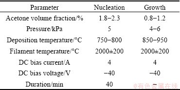
The Si (100) substrate was pretreated by abrading and roughening the surface with diamond powder and ultrasonically cleaned in deionized water and acetone before deposition. Figure 1 shows a schematic of the hot filament CVD apparatus used for CVD diamond deposition. Six tantalum wires (diameter: 0.6 mm) were arranged as an excitation hot filament, and were dragged straight by the high temperature spring. The Si substrate was held at a distance of 10 mm below the hot filament. A DC bias was applied between the filament and Si substrate to enhance the diamond nucleation and growth. The filament was referred to be the cathode (bias 50-100 V), which can produce DC discharge (current 1-3 A). The reaction gases were H2 and acetone mixed with tetraethoxysilane (TEOS). The details of typical parameters are given in Table 1.
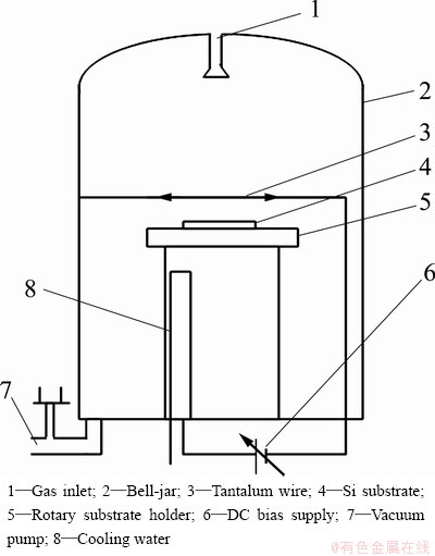
Fig. 1 Schematic illustration of hot filament CVD apparatus
Table 1 Parameters of nucleation and growth of Si-doped diamond films
After deposition, the surface morphologies of the diamond films were estimated by SEM. The ingredients and purity of the diamond films were examined by Raman spectroscopy and XRD. Surface roughness was studied with a surface profilometer. The method was to measure the average surface roughness within a 2 mm length at random place on the films. Through the study of Si-doped diamond films on Si concentration and growth time, the influence of Si doping on film quality and microstructure was systematically analyzed.
3 Results and discussion
Figure 2 shows the surface morphologies of the diamond films grown under various Si concentrations (0-1%). Apparently, a typical surface morphology of the microcrystalline diamond film can be observed under the condition of no Si doping. In this case, the film surface is rather rough, with a pyramidal morphology dominated by (111) faceted crystals, whose size reaches 5-6 ��m. When adding TEOS into the reactant gas, however, the surface morphology changes remarkably. At Si concentration of 0.2%, the film surface is covered by well-faceted diamond crystallites with grain size of 2-3 ��m, most of which have octahedral shape. When the Si to C ratio rises to 0.4%, hexagonal facets, i.e. (110) facets emerge. With the Si concentration reaches 0.6%, the morphology is dominated by rhombic shaped facets. Also, a great number of small diamond grains appear and surround the large diamond grains, as shown in Fig. 2(d). With further addition of TEOS to the reactant gas, a cauliflower-like morphology occurs, and meanwhile, a large number of refined particles present in the vicinity of grain boundary. And finally, as illustrated in Fig. 2(f), the film surface is ultimately covered by refined crystallites and smooth fine-grained diamond (SFGD) film is achieved.
The XRD pattern of the diamond films with various Si concentrations are shown in Fig. 3. According to the spectra shown in Fig. 3, six diffraction peaks are found in the spectra at 2�� values of 26.3��, 29.3��, 43.2��, 47.3��, 68.9�� and 74.6��. The peaks at 2�� value of 26.3�� and 68.9�� are identified as peaks for the amorphous carbon. The peaks at 2�� of 29.3�� and 47.3�� are attributed to the graphite. According to Fig. 3(a), i.e. pure diamond film, the first peak related to the diamond arises at 2�� of 43.2�� and it is associated to the plane (111). A second peak observed at 2�� of 74.6�� is a characteristic reflection of the plane (220). It can be noted that the peak of the plane (111) is more intense than the peak of the plane (220). When it comes to the Si-doped diamond, as shown in Figs. 3(b)-(f), however, the peak of the plane (220) becomes dramatically intense while a distinct decrease in intensity of (111) peak occurs. It illustrates that in Si-doped diamond films the formation of (111) oriented crystallites is dramatically restrained.
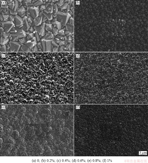
Fig. 2 SEM images of surface morphology of diamond with different Si to C ratios

Fig. 3 XRD patterns of Si-doped diamond with different Si to C ratios
The diamond films are deposited at the various deposition time and then characterized by SEM (Figs. 4 and 5), AFM (Fig. 6) and XRD (Fig. 7) in order to better understand the formation process of the SFGD films grown with Si to C ratio of 1%. As present in Fig. 4, except for the crystal growth, the morphology remains almost unchanged in the first 6 h of deposition. However, during the next 2 h, the surface grain size is dramatically refined. Figure 5 shows the cross-sectional SEM images of the conventional undoped diamond film and Si-doped SFGD film. It can be observed from Fig. 5 that the structure of Si-doped diamond film which presents near the substrate is quite similar to that of pure diamond: both have columnar structure with coarse crystalline grains. This probably means that the Si-doped diamond crystals easily grow in the first 6 h, as shown in Figs. 4(a)-(c). As the diamond crystallites continue to grow, the coarse grains and the columnar structure of the conventional undoped diamond film generally remain unchanged. In contrast, for Si-doped diamond film, the columnar structure becomes more and more tenuous when it approaches the surface of Si-doped diamond. Finally, the structure disappears when it reaches the surface and the cross-sectional structure is familiar with that padded by silver sand. This indicates that during the next 2 h the massive secondary nucleation occurs and SFGD film is synthesized. According to Fig. 6, the surface AFM image of the Si-doped SFGD film, the film is composed of refined diamond particles with grain sizes ranging from 100 to 200 nm. The film is familiar with the structure piled by silver sand rather than columnar shape. The surface roughness of the film is measured at Ra<60 nm by AFM in a 10 ��m��10 ��m scanning area.

Fig. 4 SEM images of diamond films grown at Si to C ratio of 1% with different deposition time
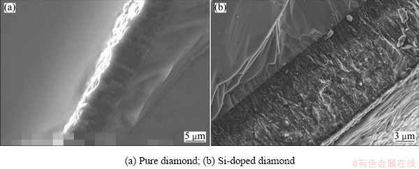
Fig. 5 Cross-sectional SEM images of diamond films
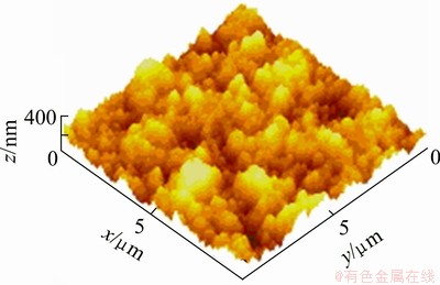
Fig. 6 Surface AFM image of Si-doped SFGD film
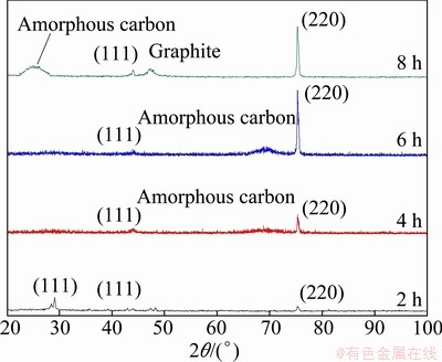
Fig. 7 XRD patterns of Si-doped diamond films at Si to C ratio of 1% with different growth time
Figure 7 shows the XRD pattern of the Si-doped diamond films at Si to C ratio of 1% with different growth time. As exhibited, for the Si-doped diamond film grown for 2 h, the peak at 2�� value of 28.5�� is attributed to the (111) silicon substrate, which can be observed because of the insufficient thickness of the sample. With the increase of growth time, the peak of diamond (220) plane becomes intense. In contrast, the peak of diamond (111) plane remains rather weak. Moreover, it can be observed that the content of amorphous carbon in the diamond films obviously increases with the growth time.
From SEM micrographs of Si-doped diamond films grown with different Si concentration and growth duration, it is observed that Si doping can affect the orientation of crystalline grains: undoped diamond film is dominated by pyramidal facets, while with the increase of Si concentration, the Si-doped diamond tends to be dominated by hexagonal or rhombic facets. Meanwhile, XRD spectra of Si-doped diamond show the inhibition of (111)-oriented facet formation. Therefore, it can be concluded from SEM and XRD analyses that Si doping can inhibit the formation of (111) oriented facets. WILD et al [17] systematically investigated the growth rate of facets and dominated orientation during CVD diamond deposition. According to their study, deposition temperature and reactant gas concentration have great influence on the growth rate of crystalline facet. Si doping may change the chemical groups in the growth atmosphere and affect the adsorption and diffusion of active groups of carbon grains during deposition.
Figures 8(a)-(f) show the Raman spectra of Si-doped diamond films with different Si concentrations.
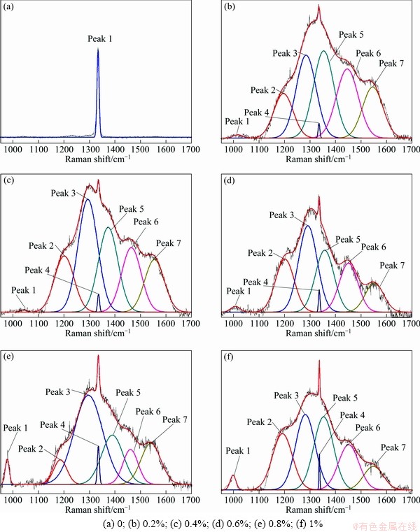
Fig. 8 Raman spectra of Si-doped diamond films with different Si to C ratios
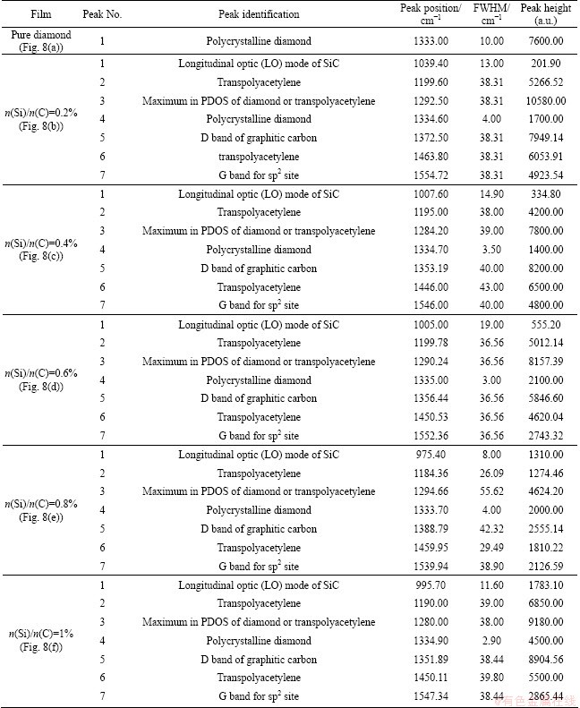
These Raman spectra have been deconvolved and analyzed by multi-Gaussian peak fitting. The results are summarized in Table 2. Each Gaussian is defined by its centre wavenumber, full-width-half-maximum (cm-1) and height. The proposed identification of the peaks in Table 2 is based on Refs. [18-20]. For undoped diamond film, the sharp and intense peak at 1333.53 cm-1, which represents the sp3-bonded carbon, indicates high phase-purity polycrystalline diamond. As for Si-doped diamond films, however, rather high proportion of non-diamond (sp2-bonded) carbon phase can be obviously observed, which suggests the decrease of diamond film quality, as shown in Figs. 8(b)-(f) and Table 2. Moreover, it can be detected that a Raman band around 1000 cm-1 appears and becomes more intense with the increase of Si concentration, which can be ascribed to SiC signal [18]. This may prove the existence of Si��C bonds in Si-doped diamond. Also, the wave numbers of the diamond peak in Raman spectra of Si-doped diamond are all slightly blue-shifted with respect to the corresponding peak in the pure CVD diamond (1333 cm-1), which means greater residual stress in Si-doped diamond films.
Table 2 Results of multi-peak fitting Raman spectra of CVD diamond films
The above results of Raman spectra can be interpreted from the following two aspects. On one side, the atomic size of Si is almost 50% larger than that of carbon. Its accommodation at a regular diamond lattice is likely to cause lattice distortion and dilatation, and thus cause compressive stress. When the lattice strain energy reaches or exceeds the defect formation energy, the stress will release and defects will come into being, which can capture more Si impurity in turn. This process causes the increase of defects and sp2 phase in Si-doped diamond. On the other side, due to Si doping, the grain size of Si-doped diamond film is smaller than that of pure diamond film, which leads to higher grain boundary density. This can produce increasing graphite-like sp2 bonded components and amorphous carbon at the grain boundaries. With the increasing proportion of non-diamond carbon phase, the internal film stress also increases. Consequently, the Si doping can promote the formation of non-diamond carbon phase (mainly amorphous carbon and graphite) and increase residual stress in polycrystalline diamond.
There are two crucial factors that contribute to the occurrence of the fine-grained crystals in the Si-doped diamond films. One is to control the crystal grain size and avoid overgrowth; the other is to increase the nucleation density during the nucleation stage. On one hand, Si doping can avert the overgrowth of crystallites. The atom mass of Si is much larger than that of carbon; so on average the particle with Si atoms carries more energy than ordinary hydrocarbon in the reaction chamber. Consequently, the particles with Si atoms bombard substrate and supply more energy to surface than particles of ordinary hydrocarbon. It is difficult for diamond grain to overgrow on the occasion of the more and stronger bombardment [21]. Also, Si doping has induced the presence of Si��C bonds in the films, which can weaken the adjacent C��C bonds and contribute to the sp2-bonded carbon phase. This also constrains the over growth of diamond crystallites. On the other hand, as noted earlier, in the reaction chamber the substrate is bombarded by the particles with Si atoms and receives more energy. The adsorbed particles with Si atoms on the substrate become more active and promote the ratio of the secondary formation of nuclei [21]. Moreover, the Si doping can greatly promote the formation of amorphous carbon in the diamond films, which can be the perfect site for diamond nucleation [22,23]. Therefore, it can be concluded that Si doping can make significant contributions to the increase of nucleation density. The above mentioned are the reasons to form the refined crystallites in Si-doped diamond films. The crystalline grain size can be greatly affected by Si concentration and growth duration. In this work, the most refined grains, i.e. SFGD crystallites, are achieved at n(Si)/n(C) ratio of 1% with growth duration of 8 h.
As for the reason large scale of the secondary nucleation occurs only after 6 h growth for the Si-doped diamond film with doping level of 1%, the followings are the reasons. The Si doping can greatly promote the formation of defects and non-diamond carbon phase in the diamond film, which can constrain the overgrowth of diamond crystals. Meanwhile, as the growth time goes on, the defects and non-diamond carbon phase, like amorphous carbon, constantly increase. As mentioned above, the amorphous carbon can be perfect site for diamond nucleation. Consequently, after 6 h deposition high quantity of non-diamond carbon phase has accumulated at the diamond grain boundaries and induced large scale of secondary nucleation. The fine grains generated from the secondary nucleation cover the initial micro diamond crystals and then SFGD film is formed.
Figure 9 shows the surface profiles and surface roughness of diamond films. The surface roughness of Si-doped diamond films is obviously smaller than that of pure diamond film, which is attributed to the relatively smaller grain size. The surface of Si-doped diamond film at n(Si)/n(C) ratio of 1% is smoother than other Si-doped diamond films. This is due to its remarkably refined crystallites.
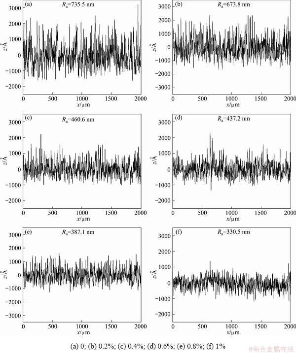
Fig. 9 Surface profiles of diamond films with different Si to C ratios
4 Conclusions
1) Si doping in the diamond films results in the change in the surface morphology from (111) facets to rhombic shaped facets, i.e. (110) facets. XRD analysis shows that Si doping dramatically inhibits the formation of (111) oriented facets, which accords with SEM study.
2) Si doping can reduce crystallite size and enhance grain refinement. When n(Si)/n(C) ratio rises to 0.6%, the second nucleation appears and the thin film ultimately attain SFGD crystallites at n(Si)/n(C) ratio of 1%. Consequently, Si-doped diamond film has lower surface roughness than pure diamond film (Ra=735.5 nm). Due to its fine-grained crystalline surface, the Si-doped diamond film grown at n(Si)/n(C) ratio of 1% has the minimum roughness (Ra=330.5 nm).
3) Si doping enhances the formation of defects and non-diamond phase in the films, which is of great importance to the secondary nucleation. Moreover, Si doping promotes Si��C bonds formation in the films. Si doping and Si��C bonds also play a role in restricting the over growth of crystallites. These are the reasons to attain grain refinement and fabricate SFGD film by Si doping.
References
[1] FAN W D, WU H, JAGANNADHAM K, GORAL B C. Wear resistant diamond coatings on alumina [J]. Surface and Coatings Technology, 1995, 72(1): 78-87.
[2] SUN Fang-hong, ZHANG Zhi-ming, CHEN Ming, SHEN He-sheng. Improvement of adhesive strength and surface roughness of diamond films on Co-cemented tungsten carbide tools [J]. Diamond and Related Materials, 2003, 12(3-7): 711-718.
[3] CHEN Ming, JIAN Xiao-gang, SUN Fang-hong, HU Bing, LIU Xue-shen. Development of diamond-coated drills and their cutting performance [J]. Journal of Materials Processing Technology, 2002, 129(1-3): 81-85.
[4] CHEN Ming, SUN Fang-hong, JIAN Xiao-gang, ZHANG Zhi-ming. Development of diamond-coated drills for high-speed machining SiC particles reinforced aluminum-matrix composite [J]. Key Engineering Materials, 2003, 259: 853-857.
[5] EINAGA Y, KIM G S, PARK S G, FUJISHIMA A. A study of the crystalline growth of highly boron-doped CVD diamond: Preparation of graded-morphology diamond thin films [J]. Diamond and Related Materials, 2001, 10(3): 306-311.
[6] KARABUTOV A V, KONOV V I, PEREVERZEV V G, VLASOV I I, ZAVEDEEV E V, PIMENOV S M, LOUBNIN E N. Competition of nitrogen doping and graphitization effect for field electron emission from SFGD films [J]. Journal of Vacuum Science & Technology B, 2004, 22: 1319-1326.
[7] LI Rong-bin. Study of the stress in doped CVD diamond films [J]. Acta Physica Sinica, 2007, 56(6): 3428-3434.
[8] OHANA T, SUZUKI M, NAKAMURA T, TANAKA A, KOGA Y. Tribological properties and characterization of DLC and Si-DLC films in aqueous environment [J]. New Diamond and Frontier Carbon Technology, 2004, 14(4): 207-216.
[9] REISEL G, DOMER-REISEL A, WIELAGE B. Silicon doped diamond like carbon as substitute for lubrication in spin-extrusion [J]. Diamond and Related Materials, 2005, 14(11-12): 1810-1814.
[10] CHOI J, NAKAO S, IKEYAMA M, KATO T. Effect of oxygen plasma treatment on the tribological properties of Si-DLC coatings [J]. Physica Status Solidi C, 2008, 5(4): 956-959.
[11] HARADA M. Structure analysis of silicon-doped diamond-like carbon films by X-ray and neutron reflectivity measurements [J]. Radioisotopes, 2010, 59(7): 451-457.
[12] ZHAO Fei, LI Hong-xuan, JI Li, QUAN Wei-long, ZHOU Hui-di, CHEN Jian-min. Preparation and characterization of Si-doped diamond-like carbon films [J]. China Surface Engineering, 2010, 23(4): 11-14.
[13] ER K H, SO M G. The mechanical and structural properties of Si-doped diamond-like carbon prepared by reactive sputtering [J]. Journal of Ceramic Processing Research, 2011, 12(2): 187-190.
[14] LAN Hui-qing, CUI Jun-hao, KATO T. Tribological property of Si-doped diamond-like-carbon films [J]. Journal of Vacuum Science and Technology, 2011, 31(1): 61-66.
[15] MUSALE D V, SAINKAR S R, KSHIRSAGAR S T. Raman, photoluminescence and morphological studies of Si- and N-doped diamond films grown on Si(100) substrate by hot-filament chemical vapor deposition technique [J]. Diamond and Related Materials, 2002, 11(1): 75-86.
[16] BARJON J, RZEPKA E, JOMARD F, LAROCHE J M, BALLUTAUD D, KOCINIEWSKI T, CHEVALLIER J. Silicon incorporation in CVD diamond layers [J]. Physica Status Solidi A, 2005, 202(11): 2177-2181.
[17] WILD C, KOHL R, HERRES N,  W, KOIDL P. Oriented CVD diamond films: Twin formation, structure and morphology [J]. Diamond and Related Materials, 1994, 3(4): 373-381.
[18] WEISHART H, HEERA V, EICHHORN F, PECZ B, TOTH L, SKORUPA W. Diamond formation by carbon implantation into cubic silicon carbide [J]. Diamond and Related Materials, 2004, 13(4-8): 627-632.
[19] FERRARI AC, ROBERTSON J. Resonant Raman spectroscopy of disordered, amorphous, and diamond like carbon [J]. Physical Review B, 2001, 64(7): 075414.
[20] FERRARI AC, ROBERTSON J. Origin of the 1150 cm-1 Raman mode in nanocrystalline diamond [J]. Physical Review B, 2001, 63(12): 121405.
[21] WANG Tao, XIN Hai-wei, ZHANG Zhi-ming. The fabrication of nanocrystalline diamond films using hot filament CVD [J]. Diamond and Related Materials, 2004, 13(1): 6-13.
[22] SINGH J, VELLAIKAL M. Nucleation of diamond during hot filament chemical vapor deposition [J]. Journal of Applied Physics, 1993, 73(6): 2831-2834.
[23] MORRISH A A, PEHRSSON PEHR E. Effect of surface pretreatment on nucleation and growth of diamond films on a variety of substrates [J]. Applied Physics Letters, 1991, 59(4): 417-419.
�����CVD���ʯ��Ĥ
������1���Ž���1���﷽��1, 2, ��־��1, 2
1. �Ϻ���ͨ��ѧ ��е�붯������ѧԺ���Ϻ� 200240��
2. ���ݽ������׳�Ӳ��Ĥ����˾������ 215000
ժ Ҫ���о�����Ӷ�CVD���ʯ��Ĥ��ò���ṹ���Ժͳɷֵ�Ӱ�졣ͨ�����ͪ�м���������������Ϊ��Ӧ���壬�ڹ�����ϳ��������CVD���ʯ��Ĥ�����ʯ��Ĥ�ı�����ò������֯�ɳ�����羵���������ʯ��Ĥ�ijɷ�ͨ����������X��������(XRD)�����о�����Ĥ�ı���ֲڶ��ɱ����������������������������ӻή�;����ߴ磬�ٽ�����ϸ����������������ò��XRD�о�������(111)����ľ����������١����������о�����������ӻ�ٽ���Ĥ�й�̼�����γ��Լ��ǽ��ʯ������ࡣ�ڹ�̼Ũ�ȱ�Ϊ1%ʱ�������õ��⻬��ϸ�������ʯ��Ĥ��
�ؼ��ʣ�����ӣ���˿��ѧ��������������ʯ��Ĥ
(Edited by Hua YANG)
Foundation item: Project (51275302) supported by the National Natural Science Foundation of China; Project (BC2012124) supported by Technical Innovation Funds for the Sci-Tech Enterprise of Jiangsu Province, China
Corresponding author: Fang-hong SUN; Tel: +86-21-34206557; Fax: +86-21-62932610; E-mail: sunfanghong@sjtu.edu.cn
DOI: 10.1016/S1003-6326(13)62821-6
Abstract: The effects of Si doping on morphology, components and structure characteristics of CVD diamond films were studied. Si-doped CVD diamond films were deposited on Si substrate by adding tetraethoxysilane (TEOS) into acetone as source of reactant gas. The morphology and microstructure of diamond films were characterized by scanning electron microcopy (SEM). The crystalline quality of diamond films was studied by Raman spectroscopy and X-ray diffractometry (XRD). The surface roughness of the films was evaluated with surface profilometer. The results suggest that Si doping tends to reduce the crystallite size, enhance grain refinement and inhibit the appearance of (111) facets. Raman spectra indicate that Si doping can enhance the formation of sp2 phase in diamond films. Moreover, Raman signal of SiC was detected, which suggests the existence of Si in the diamond films. Smooth fine-grained diamond (SFGD) film was synthesized at Si to C ratio of 1%.
