
���±�ţ�1004-0609(2007)03-0390-06
����0.10%Ce��Sn-0.7Cu-0.5Ni������Cu��������IMC��Ӱ��
¬ ������ԣ��� �ۣ��컪ΰ�����ܺ�
(���ϴ�ѧ ���Ͽ�ѧ�빤��ѧԺ����ɳ 410083)
ժ Ҫ��
�о�Sn-0.7Cu-0.5Ni-xCe(x=0��0.1)������ͭ�����543 Kǥ���Լ�453 K����ʱЧ�Խ�������仯����(IMC)���γ���������Ϊ��Ӱ�졣�����������Sn-0.7Cu-0.5Ni���ϺϽ�������0.10%Ce�������Ƶ���ʱЧ�����н���IMC���γ�����������������γɵĽ���IMCΪCu6Sn5��ʱЧ10 d��Sn-0.7Cu-0.5Ni��Sn-0.7Cu-0.5Ni-0.10Ce��2�ֺ����о���Cu3Sn�γɣ���Sn-0.7Cu-0.5Ni/Cu������ȣ�Sn-0.7Cu-0.5Ni-0.10Ce/Cu����IMC���Ϊƽ�����ý���IMC���γ�������������ɢ���ƣ���Ҫȡ����Cuԭ�ӵ���ɢ������ϡ��Ԫ��Ce������Cuԭ�ӵ���ɢ��Sn-0.7Cu-0.5Ni��Sn-0.7Cu-0.5Ni-0.10Ce�������IMC����������ʷֱ�Ϊ6.15��10-18��5.38��10-18 m2/s��
�ؼ��ʣ�
��Ǧ���������淴Ӧ������ʱЧ��IMC����������
��ͼ����ţ�TG 425.1���� ���ױ�ʶ�룺A
Effect of 0.10% Ce on intermetallic compounds at Sn-0.7Cu-0.5Ni/Cu interface
LU Bin, WANG Juan-hui, LI Hui, ZHU Hua-wei, JIAO Xian-he
(School of Materials Science and Engineering, Central South University, Changsha 410083, China)
Abstract��Intermetallic compound(IMC) formation and growth of Sn-0.7Cu-0.5Ni solder with addition 0.1% Ce were studied for Cu-substrate during soldering at 543 K and isothermal aging at 453 K. The results show that addition of 0.1% Ce into Sn-0.7Cu-0.5Ni solder inhibits the excessive formation and growth of intermetallic compounds during the soldering reaction and thereafter under aging condition. The intermetallic compound layer formed firstly at the interface is Cu6Sn5, after 10 d of aging a thin Cu3Sn layer is also observed for both solders. After several days of aging, Sn-0.7Cu-0.5Ni-0.1Ce solder gives comparatively planar intermetallic layer at the solder-substrate interface than Sn-0.7Cu-0.5Ni solder. The formation of intermetallic compounds during aging for both solders follows the diffusion control mechanism. Intermetallic growth rate constants for Sn-0.7Cu-0.5Ni and Sn-0.7Cu-0.5Ni-0.1Ce solder are 6.15��10-18 and 5.38��10-18 m2/s, respectively, which has significant effect on the growth behavior of intermetallic compounds during aging.
Key words: lead-free solder; interfacial reaction; isothermal aging��IMC; growth rate
Ŀǰ��Sn-Pb�Ͻ��Ϲ㷺Ӧ�����ִ�����װ���С�Ȼ����Pb�ж����Ի��������ǵ����彡����������Ӱ�죬����������û�������Ǧ���������溬Ǧ����[1]���ڲ��庸���У�Sn-Cu��������(Sn-0.7Cu������������%����ͬ)����Ϊ������ϣ���������Sn-Pb���ϵ���Ǧ����[2-3]����Sn-3.5Ag��Sn-3.8Ag-0.7Cu������ȣ�Sn-0.7Cu�������ϱ���Ϊ��һ�ָ������ڵ�װ���ӵĺ���[4]��Ȼ�����ú��ϵ���ʪ����Խϲ�������ܺܺõغ��ӣ���Լ���ڵ���ӡˢ��·��(PCB)�Ȳ��庸���е�Ӧ�á�����������Ҫ��ͨ������Ag��Ni��P���������ɿ���[5-7]���о��������[7]����Sn-0.7Cu���ϺϽ��У�����NiԪ�ص�Ч����ã�Ni�����ܸı����ں����н����仯����(IMC)����״�����⺸��ʱ���ֺ���������ȱ�ݣ����ҵ�Ni���������ߴ�0.5%ʱ�����ϻ����кõ��������ܺ���俹����
��ǥ�������У��ۻ��ĺ�������巴Ӧ����ǥ�����洦�γɽ��������������(IMC)��IMC���γ�һ�������ǥ�������ɿ���������ͨ������巴Ӧ�γɽϱ���IMC�������ڻ�����õ�ұ���ϣ���һ���棬��IMC��̫������������Ч��[8-9]����ϡ��Ԫ��Ce��ϸ��Sn-Ag-Cu���ϺϽ���֯���������ƺ��ϺϽ���Cu������IMC������[10]�����������ǥ�������Ŀɿ��ԡ�Ŀǰ����δ��ϡ��Ԫ��Ce��Sn-0.7Cu-Ni���ϺϽ���Cu������IMC���γɺ�������Ӱ��ı������ڴˣ�����������Sn-0.7Cu-0.5Ni���ϺϽ�Ϊ�о�����̽��ϡ��Ԫ��Ce��Sn-0.7Cu-0.5Ni/Cuǥ����ͷIMC���γ��Լ�����ʱЧ������IMC������Ӱ�죬����Ϊ�о�ϡ��Ԫ������Ǧ�����е������ṩʵ�����ݡ�
1��ʵ��
ʵ����ԭ����Ϊ���ȸ���99.9%�ĵ��ʽ���Sn��Sn-10%Cu��Sn-4.7%Ni�Լ�Sn-3.7%Ce���м�Ͻ𡣰�Sn-0.7Cu-0.5Ni-xCe(x=0, 0.1)����ɷ���ú�����ո�Ӧ����¯�������������¶�Ϊ873~923 K��
ǥ������ߴ�Ϊ15 mm��3 mm��15mm(W��D��L)������Ϊ99.9%��CuƬ�����������5% NaOH��Һ������ˮ��ϴ�������������Ϊ5% HClˮ��Һ��ϴ��Ȼ��������ˮ��ϴ����ͭƬ��Ϳ��һ���������������(RMA)������������������Sn-0.7Cu-��0.5Ni-xCe(x=0��0.1)������Ʒ������Cu�����ϣ�����������м��ȣ���543 K����5 min����������Ʒ�ۻ����ǥ��̬��Ʒ��������2�ֳɷֵ�ǥ��̬��Ʒ�������ʿ��и�ɳߴ�Ϊ3 mm��3 mm��8 mm(W��D��L)����Ʒ���ֱ����������н���ʱЧ������������Ŀ��¾���Ϊ��1 K��ǥ��̬��Ʒ����453 K�ֱ����ʱЧ5��10��20 d��ȡ�����䡣Ϊ�˱��ڽ���IMC���о�����Ʒ����Ƕ�ڻ�����֬���ĥ���⣬��ʴ����ʴҺΪ95% C2H5OH+5% HCl���Һ����KYKY2800ɨ���������(SEM)�Ϸ���IMC������֯�����������ȡ���ÿ����Ʒ����30�Σ�ȡ��ƽ��ֵ��
2�����������
2.1�����������֯�ı仯
ͼ1��ʾΪSn-0.7Cu-0.5Ni-xCe(x=0��0.1)����/Cu�����543Kǥ��̬�����ͷ����֯��SEM��Ƭ�����Կ�����������Cu����������γ�IMC�㡣EDX�����������������/Cu��������IMCΪCu6Sn5�ࡣ���⣬���۲쵽����IMC��Ļ������γ�һЩ�ִ��Cu6Sn5�࣬�������Sn-0.7Cu-0.5Ni/Cu��ϵ���ԣ�Sn-0.7Cu-0.5Ni-0.1Ce/Cu������ϵ�Ļ��������γɵ�Cu6Sn5�����������(��ͼ1��2)���������������Sn-0.7Cu-0.5Ni-xCe(x=0��0.1)/Cu��ǥ������Cu6Sn5���ȷֱ�Ϊ1.95 ��m(x=0)��1.73 ��m(x=0.1)����ǥ�������У������е�Cuԭ������ɢ��ʽͨ������Cu6Sn5������ۻ��ĺ��ϻ����С���Cuԭ�����ۻ������еĸ���������ijһ��С�ٽ�ֵʱ��������Cuԭ�Ӿͻ��뺸�ϻ����е�Snԭ�ӷ�Ӧ����Cu6Sn5��������ǥ�����渽���ĺ��ϻ������γ�һЩ�ִ��Cu6Sn5�ࡣʵ����������ϡ��Ԫ��Ce������Cuԭ����Sn-0.7Cu-0.5Ni����/Cu����Ľ���IMC������ɢ��

ͼ1 543 Kǥ������/Cu�����۽ṹ��SEM��Ƭ
Fig.1 SEM images of solder/Cu interfaces after soldering at 543 K: (a) Sn-0.7Cu-0.5Ni solder; (b) Sn-0.7Cu-0.5Ni-0.10Ce solder

ͼ2 543 Kǥ�����ϻ�����IMC���γ�
Fig.2 Formation of intermetallic compound in bulk of solder after soldering at 543 K: (a) Sn-0.7Cu-0.5Ni solder; (b) Sn-0.7Cu- 0.5Ni-0.10Ce
ͼ3��ʾΪSn-0.7Cu-0.5Ni-xCe(x=0��0.1)/Cuǥ�����澭��180 ��/ʱЧ5 d��ı�ɢ��SEM��Ƭ�����Կ���������453 K/5 dʱЧ����IMC�ĺ�ȷֱ�����3.26 ��m(x=0)��2.98 ��m(x=0.1)�������ڵ��ȱ���IMC�ȵף�IMC�������ٶȸ��ڷ嶥�������ٶȣ�����Lee��[11]�����Ľ����һ�¡�ʱЧ5 d����IMC����̬��������ȱ�״(��ͼ1)���Ϊƽ����ƽ��״ת��(��ͼ3)�����⣬ʱЧ5 d��δ�ڽ���IMC�з���Cu3Sn�࣬��������������Sn-Pb��������/Cu�����о���ȴ���Է�����Cu3Sn�γ�[12]���������ǥ����ͷ��Ӧ����߲�����Cu3Sn�dz�������С�йأ�����ʵ����δ���ֽ���IMC���е�Cu3Sn�ࡣ

ͼ3 453 K/5 dʱЧ����/Cu��ͷ����֯��SEM��Ƭ
Fig.3 SEM images showing solder/Cu interfaces after 5 d of aging: (a) Sn-0.7Cu-0.5Ni solder; (b) Sn-0.7Cu-0.5Ni- 0.10Ce
��һ�����ӵ���ʱЧʱ�䣬������Cu6Sn5�������Cu������ֲ�״��Cu3Sn�ࡣͼ4��5��ʾ�ֱ�Ϊ453 KʱЧ10 d��20 d��ı�ɢ��SEM��Ƭ�����Կ���������/Cu����IMC�����ֳ�Cu6Sn5��Cu3Sn�ĸ���ṹ����Sn-0.7Cu- 0.5Ni/Cu��IMC����ò��Sn-0.7Cu-0.5Ni-0.10Ce/Cu�IJ���ò�ֲںͲ�ƽֱ��EDX�������֤ʵ��IMC���е�Cu6Sn5������ϲ࣬Cu3Sn���Cu���ײࡣ����Sn��Cu6Sn5���е���ɢϵ������Cu��Cu6Sn5���е���ɢϵ��������ͨ������Cu6Sn5���Sn���٣������е�Cu��IMC������ɢ������Cu6Sn5������Ӧ���ڽ���Cu6Sn5�������γ�Cu3Sn��(��ͼ4(b)��5(b))������Tu��[13]�ı���������Ǻϡ����⣬EDX�����������ʾ������Cu6Sn5���к���һ����Ni(��ԭ�ӷ���Ϊ4.3%)������(Cu,Ni)6Sn5��ѧ��ȣ�˵���ý���Cu6Sn5��ӦΪ(Cu,Ni)6Sn5�Ͻ��࣬(Cu,Ni)6Sn5��NiԪ��Ӧ���Ժ����С����ں����к��нϸߵ�Ni(��������Ϊ0.5%)���ڷ�Ӧ��ʼ�Σ�Sn-Cu-Ni�����е�Niԭ����Sn��Cu6Sn5���е���ɢһ���������Cu6Sn5����ɢ���ҿɲ�����淴Ӧ�γɺϽ�IMC���ڻ���ѭ�������У�Zhang��[14]Ҳ����Ni�ܹ���ɢ���������Ͻ�ͷ���γ�(Cu,Ni)6Sn5��Ԫ�ࡣ
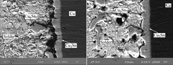
ͼ4 453 KʱЧ10 d����/Cuǥ����ͷ����֯��SEM��Ƭ
Fig.4 SEM images showing the solder/Cu interfaces after aged at 453 K for 10 d: (a) Sn-0.7Cu-0.5Ni sloder; (b) Sn-0.7Cu- 0.5Ni-0.10Ce
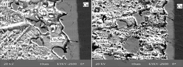
ͼ5 53 K/20 dʱЧ����/Cu��ͷ����֯��SEM��Ƭ
Fig.5 SEM images showing solder/Cu interfaces after aged at 453 K for 20 d: (a) Sn-0.7Cu-0.5Ni solder; (b) Sn-0.7Cu- 0.5Ni-0.10Ce
��ͼ4��5�������IMC��ȡ��������������ʱЧʱ������ӣ���������IMC������������10 d����ʱЧ����IMC���ܺ�ȷֱ�����4.34 ��m(x=0)��3.97 ��m(x=0.1)����20 d����ʱЧ����IMC���ܺ�ȷֱ�����5.21 ��m(x=0)��4.78 ��m(x=0.1)��
2.2 ����ʱЧ�����к���/Cu�����IMC������
��ʱЧ�����У����γɵĽ���IMC�ĺ����ʱЧʱ��Ĺ�ϵ�����������������ʽ��������

Kim��[15]��Ϊ���ڹ�̬ʱЧʱ������IMC������һ����ѭ���Ի��������߹��ɱ仯�����������ܵ������ط��ķ�Ӧ���ʿ���ʱ��IMC��������ѭֱ�߹��ɡ���֮��IMC�������ܵ���ɢ����ʱ����ѭ�����߹��ɡ���������ɢ���ƵĹ��̣�����IMC���������Ӧ����ѭʱ���ƽ�����Ķ���ѧ���ۣ����ҿ��Ա���ΪY=kt0.5����ʱʱ��ָ��nΪ0.5[16]��
ͼ6��ʾΪSn-0.7Cu-0.5Ni-xCe(x=0��0.1)/Cuǥ������IMC����ܺ����ʱЧʱ���ƽ�����ĺ�����ϵ�����Կ�����IMC���ȵ�������ʱЧʱ���ƽ�������Ƴ�ֱ�߹�ϵ����Sn-0.7Cu-0.5Ni/Cu������ϵ��IMC����������ʸ���Sn-0.7Cu-0.5Ni-0.10Ce/Cu������ϵ���������ʡ�ͼ����ʾ����2�ֺ�����ϵ��IMC�����������ѭ�������������ɣ���IMC��������Ϊ����ɢ���̿���[17-19]��

ͼ6 IMC�ܺ����ʱЧʱ���ƽ�����Ĺ�ϵ
Fig.6 Thickness of intermetallic compound layer as function of square root of aging time
Ϊ�˽�һ���˽�Sn-0.7Cu-0.5Ni-xCe(x=0��0.1)/Cu������ϵ��IMC��������Ϊ����Y��Ӧt0.5�Ĺ�ϵ���ɶ�Ԫ���Իع������������������k��ͼ6��ʾΪSn-0.7Cu-0.5Ni-xCe(x=0��0.1)/Cuǥ������IMC�ܺ����ʱЧʱ��ƽ�����Ĺ�ϵ��ͼ����ʾ������б�ʼ�ΪSn-0.7Cu-0.5Ni/Cu��Sn-0.7Cu-0.5Ni-0.10Ce/Cu������ϵ�е�k���ֱ�Ϊ6.15��10-18 m2/s��5.38��10-18 m2/s���ɼ����ں���ʱЧ�����У�Sn-0.7Cu-0.5Ni/Cu���ϺϽ���ϵ��IMC���������Ը���Sn-0.7Cu-0.5Ni-0.10Ce/Cu������ϵ�������ʡ��ɴ�Ҳ���Կ�������ϡ��Ce�������ƽ���IMC���������á����Իع�ϵ��R2������ƽ�����ܺ������Իع��ƽ�����ܺ͵ı��ʣ���ֵ��Sn-0.7Cu-0.5Ni/Cu��Sn-0.7Cu-0.5Ni-��0.10Ce/Cu��ϵ�зֱ�Ϊ0.990 0��0.990 3���˱�����2�ֺ�����ϵ��IMC���γɽ�����ѭ��ɢ���ɡ�
�ں���ʱЧ�����У���IMC�����йص�ʱ��ָ��n������ʽ����[20]��
ʽ(2)�Ķ�������ʽΪ
![]()
ͼ7��ʾΪln(Yt-Y0)��lnt�Ĺ�ϵ�������ߵ�б�ʿɵõ�Sn-0.7Cu-0.5Ni-xCe(x=0��0.1)/Cu���ϺϽ���ϵ��n�ֱ�Ϊ0.55��0.54��n������ɢ���̵�Ӱ��ܴӶ�ҲӰ��Sn-0.7Cu-0.5Ni-xCe(x=0��0.1)/Cu������ϵ��IMC���γɡ��������õ�IMC�������ʵ�ƽ��ֵk2���������ϵ��R2��ʱ��ָ��n����1��

ͼ7 ln(Y�CB)�� lnt�Ĺ�ϵ
Fig.7 Relationship between ln(Y�CB) and lnt
��1 �������õ�IMC�������ʵ�ƽ��ֵk2���������ϵ��R2��ʱ��ָ��n
Table 1 Calculated square of growth rate constants (k2), linear correlation coefficients (R2) and time exponent n

�ɱ�1��֪�� IMC����ȡ����Cuԭ�ӵ���ɢ���̣���Cu��Sn-0.7Cu-0.5Ni/Cu��ϵ�е���ɢ�ٶ�Ҫ����Sn-0.7Cu-0.5Ni-0.10Ce/Cu��ϵ����ɢ�ٶȡ���ǥ����Ӧ�������ڻ����е�Cuԭ���뺸�ϻ����е�Snԭ�ӷ�Ӧ�����ں�������Ľ����Լ����ϻ������γ�IMC��Cuԭ��ͨ��IMC������ɢ��������ˣ����淴Ӧ��û�п쵽����������ɢ����Cuԭ�ӣ�����û�з�Ӧ���Cuԭ��������ɢ�����ϻ�����ڲ���Sn��Ӧ����Cu6Sn5�ࡣ��ˣ����Ż�����Cuԭ�ӵļ��٣������и����Cuԭ�����ϻ�������ɢ�����⣬��������Cuԭ�ӵ��ܽ�Ƚ���ʱ��Cu6Sn5����������Ѿ��γɵ�IMC���������������IMC�������ӡ�
3 ����
1) ��ǥ����ͷ���淴Ӧ�У�����ʱЧʱ����ӳ������淴Ӧ������Cu6Sn5������Cu6Sn5+Cu3Sn˫��IMCת�䣬�Ҹ�2�ֺ��Ͻ���IMC����Ҳ���������ӣ�����Sn-0.7Cu-0.5Ni���ϺϽ�/Cu��ϵ���γɵ�IMC����Դ���Sn-0.7Cu-0.5Ni-0.10Ce���Ϻ� ��/Cu��ϵ�ĺ�ȡ�
2) Sn-Cu����IMC���γɺ�����ȡ����Cuԭ�Ӵӻ�����������е���ɢ������ϡ��Ԫ��Ce�ܽ���Sn-0.7Cu-0.5Ni/Cu�н���IMC�������ʣ�����IMC��������Sn-0.7Cu-0.5Ni����������Ϊk2��6.15��10-18��m2/s��Sn-0.7Cu-0.5Ni-0.10Ce����������Ϊk2��5.38��10-18��m2/s��
REFERENCES
[1] �¹�������С�࣬��־ͦ. ������Ǧ���ϺϽ�Sn-Zn-Ga���о�[J]. ϡ�н��������빤�̣�2004��33(11)��1222.
CHEN Guo-hai, LI Xiao-yan, GENG Zhi-ting. The study on the new type lead-free solder alloys Sn-Zn-Ga[J]. Materials and Engineering of Rare Metal, 2004, 33(11): 1222.
[2] Chen W T, Lee S W, Yip M C. Mechanical properties and intermetallic compound formation at the Sn/Ni and Sn-0.7wt.%/Ni joints[J]. Journal of Electronic Materials, 2003, 32(11): 1284-1289.
[3] Zeng K, Tu K N. Six cases of reliability study of Pb-free solder joints in electronic packaging technology[J]. Mater Sci Eng R, 2002, 38(2): 55-105.
[4] Yoon J W, Kim S W, Jung S B. Interfacial reaction and mechanical properties of eutectic Sn-0.7Cu/Ni BGA solder joints during isothermal long-term aging[J]. Journal of Alloys and Compounds, 2005, 391: 82-89.
[5] ����������. ���ӷ�װ��Ǧ��������չ[M]. ӡˢ��·��Ѷ��2004(3)��52-59.
TIAN Min-bo, MA Peng-fei. The Summarization of Lead-Free Technology in Electronic Packing[M]. Printed Circuit Board Information, 2004(3): 52-59.
[6] �� �£����������ż���, ��. һ�ָ�����ʵ����Sn-Cu��Ǧ����ǥ��[J]. ����Ԫ�������, 2004��24(4)��54-56.
YAN Yong, JIANG Xiao-hu, ZHANG Ji-zhong, et al. High performances Sn-Cu electronic lead-free solder[J]. Electronic Components and Materials, 2004, 24(4): 54-56.
[7] Huh S H, Kim K S, Suganuma K. Effect of Ag addition on the microstructure and mechanical properties of Sn-Cu eutectic solder[J]. Materials Transactions, 2001(42): 739-744.
[8] Yoon J W, Lee Y H, Kim D G, et al. Intermetallic compounds layer growth at the interface between Sn-Cu-Ni solder and Cu substrate[J]. Journal of Alloys and Compounds, 2004, 381: 51-157.
[9] ���ڽܣ��Ͻ�����Ѧ�ɰ�. �뵼�弤����ǥ��Sn-Ag-Cu��������֯[J]. ���ϴ�ѧѧ������Ȼ��ѧ�棬2006, 37(2): 229-234.
HAN Zong-jie, JU Jin-long, XUE Song-bai. Microstructures of Sn-Ag-Cu lead-free soldered joints with diode-laser soldering[J]. J Cent South Univ: Science and Technology, 2006, 37(2): 229-234.
[10] Wu C M L, Yu D Q, Law C M T, et al. Properties of lead-free solder alloys with rare earth element additions[J]. Mater Sci Eng, 2004, 44: 1-44.
[11] Lee T Y, Choi W J, Tu K N. Morphology kinetics and thermodynamics of solid-state aging of eutectic Sn-Pb and Pb-free solders (Sn-3.5Ag,Sn-3.8Ag-0.7Cu,Sn-0.7Cu) on Cu[J]. Journal of Materials Research, 2002, 17(2): 291-301.
[12] Hwang C W, Lee J G, Suganuma K, Mori H. Interfacial microstructure between Sn-3Ag-xBi alloy and Cu substrate with or without electrolytic Ni plating[J]. Journal of Electronic Materials, 2003, 32(2): 52-62.
[13] Tu K N, Thompson R D. Kinetics of interfacial reaction in bimetallic Cu-Sn thin films[J]. Acta Materialia, 1982, 30(5): 947-952.
[14] Zhang F, Li M, Chum C. Influence of substrate metallization on diffusion and reaction at the under-bump metallization/solder interface in flip-chip packages[J]. Journal of Materials Research, 2002, 17(11): 2757-2760.
[15] Kim D G, Jung S B. Interfacial reaction and growth kinetics for intermetallic compounds layer between In-Sn solder and bare Cu substrate[J]. Journal of Alloys and Compounds, 2005, 386: 151-156.
[16] Lee C Y, Lin K L. Preparation of solder bumps incorporating electroless nickel-boron deposit and investigation on the interfacial interaction behavior and wetting kinetics[J]. Journal of Materials Science, 1997, 8(6): 377-383.
[17] Vianco P T, Xilgo A C, Grant R. Intermetallic compound layer growth by solid state reactions between 58Bi-42Sn solder and copper[J]. Journal of Electronic Materials, 1995, 24(10): 1493-1505.
[18] Chen C C, Lin A H, Luo G L, Kao C R. Long-term aging study on the solid-state reaction between 58Bi-42Sn solder and copper[J]. Journal of Electronic Materials, 2000, 29(5): 1200-1206.
[19] Rizvi M J, Chan Y C, Bailey C, et al. Effect of adding 1wt% Bi into the Sn-Ag-Cu solder sally on the intermetallic formations with Cu-substrate during soldering and isothermal aging [J]. Journal of Alloys and Compounds, 2006, 407: 208-214.
[20] Vianco P T, Rejent J A. Properties of ternary Sn-Ag-Bi solder alloys: thermal properties and micro structural analysis [J]. Journal of Electronic Materials, 1999, 28(10): 1127-1137.
������Ŀ������ʡ�Ƽ��ص㹥����Ŀ(01YJJ2056)
�ո����ڣ�2006-08-25�������ڣ�2006-11-19
ͨѶ���ߣ�¬�����ڣ��绰��0731-8836319��E-mail��luoffice@mail.csu.edu.cn
[1] �¹�������С�࣬��־ͦ. ������Ǧ���ϺϽ�Sn-Zn-Ga���о�[J]. ϡ�н��������빤�̣�2004��33(11)��1222.
[5] ����������. ���ӷ�װ��Ǧ��������չ[M]. ӡˢ��·��Ѷ��2004(3)��52-59.
[6] �� �£����������ż���, ��. һ�ָ�����ʵ����Sn-Cu��Ǧ����ǥ��[J]. ����Ԫ�������, 2004��24(4)��54-56.
[9] ���ڽܣ��Ͻ�����Ѧ�ɰ�. �뵼�弤����ǥ��Sn-Ag-Cu��������֯[J]. ���ϴ�ѧѧ������Ȼ��ѧ�棬2006, 37(2): 229-234.
