
Trans. Nonferrous Met. Soc. China 25(2015) 4008-4017
Effect of Ba0.5Bi0.5Fe0.9Sn0.1O3 addition on electrical properties of  thick-film thermistors
Yun YANG1, Chang-lai YUAN1, Guo-hua CHEN1, Tao YANG1, Ying LUO2, Chang-rong ZHOU1
1. School of Materials Science and Engineering, Guilin University of Electronic Technology, Guilin 541004, China;
2. School of Information and Communication, Guilin University of Electronic Technology, Guilin 541004, China
Received 6 January 2015; accepted 30 August 2015
Abstract:
Thick-film thermistor with negative temperature coefficient (NTC), low room-temperature resistivity and modest thermistor constant was screen-printed on the alumina substrate by the combination of  with Ba0.5Bi0.5Fe0.9Sn0.1O3. The electrical properties of the thick films were characterized by a digital multimeter, a Keithley 2400 and an impedance analyzer. The results show that with the Ba0.5Bi0.5Fe0.9Sn0.1O3 content increasing from 0.05 to 0.25, the values of room-temperature resistivity, thermistor constant and peak voltage of the thick films increases and are in the ranges of 1.47-26.5 ����cm, 678-1345 K and 18.9-47.0 V, respectively. The corresponding current at the peak voltage of the thick films decreases and is in the range of 40-240 mA. The impedance spectroscopy measurement demonstrates that the as-prepared thick films show the abnormal electrical heterogeneous microstructure, consisting of high-resistive grains and less resistive grain boundary regions. It can be concluded that the addition of Ba0.5Bi0.5Fe0.9Sn0.1O3 into improves the thermistor behavior and but also deteriorates the current characteristics.
Key words:
NTC thick films; ; Ba0.5Bi0.5Fe0.9Sn0.1O3; electrical property;
1 Introduction
Negative temperature coefficient (NTC) thermistors have been widely used in modern electronic industry as temperature compensation devices, temperature sensor devices, surge protection devices, self-heating application, and infrared detecting bolometers in bulk and thick films [1-4]. Bulk thermistor materials are gradually fading away from the electronic market due to the large size. Thick-film thermistors are the current trend due to being satisfactory for the need of small-size devices in highly integrated microelectric circuits and low-cost preparation technology in the thick-film producing processes. But problems with low linearity between the reciprocal of absolute temperature and logarithmic resistance, and high-cost conductive phase of the sensor due to the use of ruthenate occur. Simultaneously, most of the thick films without the addition of ruthenate own high room-temperature resistance, limiting the application range in electronic devices. It is well known that Mn-Ni-O thermistor thick-film system with spinel structure of a general formula AB2O4 has been extensively studied for a long time [5-7]. In current literatures, NiMn2O4-LaNiO3 nanocomposite thick films show good thermistor characteristics with the room temperature resistivity (��25) of 35 k����cm and thermistor constant (��25/85) of 5000 K, where NiMn2O4 is the resistive phase and LaNiO3 acts as the conductive phase [8]. In conventional Mn-Co- Ni-O spinel system, the ��25 of the thick films was in the range of 23-7450 k����cm and the ��25/85 was in the range of 1492-4335 K [9]. Other addition such as Fe, Al, Zn, Mg and Cu in Mn-Ni-O and Mn-Co-Ni-O film systems can also tune the values of ��25 and ��25/85 based on the practical need in industrial application [10�C13]. However, the added elements can��t decrease the room-temperature resistivities of the thick films and partly give rise to the increase of ��25 value. It is very necessary to add the high-conductive Ru-based oxides/compounds into the thermistor phase for the reduction of the room- temperature resistivities of thick films [14]. It was reported that the Mn1.85Ni0.8Co0.35O4 thermistor films containing 42% RuO2 (out of the total functional phase of the paste) showed low room-temperature sheet resistance (~1 k����cm) and modest thermistor constant (~1260 K) [15]. However, it was also observed that most of the thick-film NTC thermistors containing higher RuO2 content illustrated weak linearity between the logarithmic resistance/resitivities (lg R/lg ��) and the reciprocal of absolute temperature (1/T) [16]. This denoted that Ru-based oxides/compounds were not a good conductive agent for the preparation of thick-film NTC thermistor with low room-temperature resistivities. Currently, it still needs to obtain thick-film NTC thermistors with low room-temperature resistivities, modest thermistor constant and perfect lg R-1/T linearity.
Therefore, a Ru-free thick-film NTC thermistors composed of perovskite resistive phase Ba0.5Bi0.5- Fe0.9Sn0.1O3 [17] and high conductive  [18] were fabricated by screen- printing procedures. The microstructures, electrical properties and impedance characteristics of the thick films were evaluated and discussed in terms of the resulting properties of thick-films.
2 Experimental
2.1 Preparation of thick films
(abbreviated as BCCB) source powder was produced by mixing, grinding and firing the precursors BaCO3, Bi2O3 and Co3O4. The mixtures were fired at 700 ��C for 2 h. Ba0.5Bi0.5- Fe0.9Sn0.1O3 (abbreviated as BBFS) source powder was produced by firing the precursors BaCO3, Bi2O3, Fe2O3 and SnO2 at 1050 ��C for 4 h. The thermistor pastes (ink) were prepared by mixing the desired amounts of produced and Ba0.5Bi0.5Fe0.9- Sn0.1O3 ((1-x)�CxBa0.5Bi0.5Fe0.9- Sn0.1O3, where x represents the molar ratio) source powders with the organic vehicle in order to obtain printable pastes (as shown in Table 1). The organic vehicle was a solution of ethyl cellulose, lecithin and 2-(2-butoxy ethoxy-ethyl) acetate. The mass ratio of inorganic to organic was kept at 7:3. The resultant thick-film thermistor pastes were screen-printed onto a 96% alumina substrate using a stainless screen of 58 ��m, then settled down and dried under IR lamp for 10-15 min. This printing process was repeated ten times and the thickness of each printing was 4-6 ��m. The printed patterns were fired in a muffle furnace at moderate temperatures (as shown in Table 1) with a dwell time of 60 min. All the organic components were decomposed after printing the films during the sintering process of thick films.
2.2 Characterizations of thick films
The samples were routinely characterized by X-ray diffraction (XRD) and scanning electron microscopy (SEM) equipped with energy disperse spectroscopy (EDS). The thickness of the fired films was ~50 ��m as measured by an XP-100 high resolution stylus-type surface profilometer. The DC electrical resistance of thermistor films was measured using a digital multimeter (Fluke 45) from 25 to 180 ��C with a step of 20 ��C. I-U characteristics of the thick films were measured by a Keithley 2400. For all the thick films, impedance spectra were taken at room temperature using an Agilent (4294A) Impedance Analyzer with computer controlled automated data collection, which increased the frequency logarithmically from 40 Hz to 50 MHz.
3 Results and discussion
3.1 Microstructures
Figure 1(a) shows the XRD patterns of the BCCB-BBFS composite thick films at room temperature. The thick films adopt the pure monoclinic and cubic Ba0.5Bi0.5Fe0.9Sn0.1O3 phases. No any secondary phase forms, which indicates that no any chemical reaction occurs. With increasing the mole ratio of composition (x), the intensities of diffraction peaks ascribed to BBFS phase show slight increase, which is in well agreement with the predesigned compositions shown in Table 1.
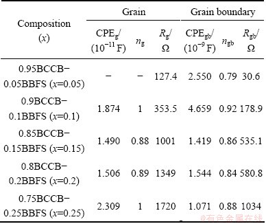
Table 1 Sintering temperatures and values of ��25, ��25/85, Ea, Um, I0 and p for various thick films
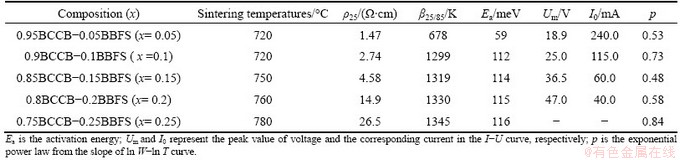
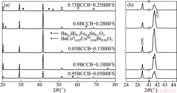
Fig. 1 XRD patterns of screen-printed thick films at 2�� of 20��-80��(a) and 25��-45��(b)
As for the diffraction intensities of (200) and (220) crystal indices for BCCB phase, the intensity of (200) crystal index decreases with increasing the BBFS content with the x value in the range of 0.05-0.15, as compared with that of (220) in Fig. 1(b). This suggests that the preferential growth orientation of the BCCB phase shifts to the (220) crystal index from the (200) face with the rise of BBFS content. The further addition of BBFS up to x=0.20 induces the abrupt rise of peak intensity of (200) relative to that of (220). It is confirmed that when the content of BBFS is relatively low, the BCCB phase is sufficient to grow along the (220) face with no limitation during the processes of grain growth. However, when the content of BBFS is high, the BBFS grains have the chance to grow by itself and therefore hinder the continuing crystal growth of BCCB grains along the initial orientation. But more detailed investigation should be conducted to confirm the above deduction for abnormal orientation behavior of BCCB phase.
Figure 2 shows the SEM images of BBFS and BCCB powders and the thick film surfaces, and the enlarged SEM image of the composition with x=0.25. From Figs. 2(a) and (b), it can be seen that the grain size of BCCB powder is comparatively larger than that of BBFS powder. It is also found that the abnormal grains and unclear grain boundaries exist in each of the composite films, due to the fact that the BBFS phase is completely or partly melted by low-melting point BCCB phase. When the BBFS content is lower, the BBFS phase is approximately melted by BCCB phase and many large molten grains containing the BCCB and BBFS phases form. With further increasing the BBFS content in the thick films, the large molten grains tend to reduce and small grains begin to occur, as illustrated in Fig. 2(h). This is due to the fact that the individual BBFS grain tends to independently grow at higher BBFS content and then acts as a grain growth inhibitor of low-melting BCCB phase.
3.2 R-T characteristics
The logarithmic resistivity (lg ��) of the BCCB- BBFS composite films as a function of the reciprocal of absolute temperatures are plotted in Fig. 3. The logarithmic resistivity of all the thick films increases linearly with increasing the reciprocal of temperature, which confirms that the as-sintered films follow the Nernst-Einstein relation. The most important characteristic parameters for practical application such as room-temperature resistivity (��25), thermistor constant (��25/85) and activation energy (Ea) are summarized in Table 1. The values of ��25/85 and Ea are calculated by Eqs. (1) and (2) as follows:
��25/85=(ln ��1-ln ��2)/(1/T1-1/T2) (1)
where ��1 and ��2 are the resistivities measured at the absolute temperatures of T1 (298 K) and T2 (358 K), respectively.
Ea=��25/85��kB (2)
where kB is the Bolzman constant. The room-temperature resistivity of the as-sintered films is 1.47 ����cm and it increases to 26.5 ����cm as the BBFS content increases up to x=0.25. The activation energies of the as-sintered films with compositions x=0.05, 0.1, 0.15, 0.2 and 0.25, are 59, 112, 114, 115 and 116 meV, respectively. Accordingly, the thermistor constants are 678, 1299, 1319, 1330 and 1345 K, respectively. The reasons for the rise of thermistor constant and activation energy following increasing the BBFS content are difficult to be clearly elucidated but are presumably related to the transformation toward high crystallinity of BBFS grains and the expanded film area of grain boundaries as observed in Figs. (1) and (2). It is known that the crystallinity of BBFS compound acting as high-resistive phase tends to increase with increasing the BBFS content in composite films and then the barrier height of thick films also rises, resulting into a significant increase of room-temperature resistivity of the thick-film thermistors.
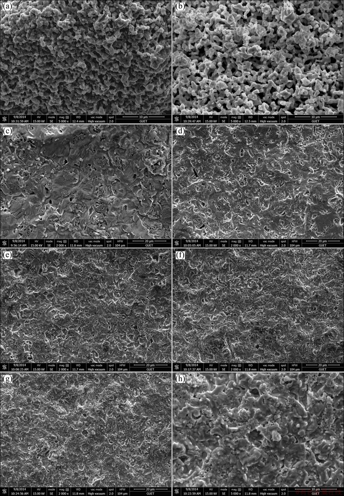
Fig. 2 SEM images of BBFS powders (a), BCCB powders (b), and surfaces of thick films with compositions of x=0.05 (c), x=0.10 (d), x=0.15 (e), x=0.20 (f) and x=0.25 (g, h)
To determine and elucidate the character of hopping motion, the ��-T data were analyzed following a procedure described by SHKLOVSKII and EFROS [19], where it is possible to determine the exponential power law (p) from the slope of a plot of ln W versus ln T, and W is defined as follows:
 (3)
(3)
where T0 is a characteristic temperature.
This is a powerful technique to elucidate the character of hopping motion. All the ln W�Cln T slope curves of the thick films are shown in Fig. 4 and the p values for all the thick films are listed in Table 1. It is found that most of the data in the slope curves in Fig. 4 are very scattering. This is due to the fact that it is a differentiation method and therefore sensitive to the scatter in the original ��-T data. The p values of composite films containing compositions with x=0.05, 0.15 and 0.2 are close to 0.5, and those of the films with x=0.1 and 0.25 are within the range of 0.5-1. For conventional VRH (Variable-Range Hopping), 0.25 VRH. It is well known that VRH motion can be further divided into Mott-VRH (p=1/3) and ES (Efros- Shklovskii)-VRH (p=1/2) [17]. For the conduction of the films with x=0.05, 0.15 and 0.2, it is more accurate to be described by ES-VRH. Considering that the p values of composite films containing compositions with x=0.1 and 0.25 are rather high exponents for general ES-VRH, here it is deduced that the hopping type might be a transition from ES-VRH to NNH.
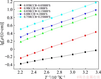
Fig. 3 Relationship between lg �� and reciprocal of absolute temperature for composite NTC thick films
3.3 I-U characteristics
Current-voltage (I-U) behavior is one of the most interesting properties in NTC thermistors, which is an indicative of the voltage drop ��U�� as the increase of DC current ��I�� through the device. Figure 5 illustrates the typical I-U curves of the thick-film NTC thermistors at 25 ��C. The curves were obtained after sufficient time remaining in the thermistors to arrive at a steady state. In Fig. 5, the peak values of voltage occur at some currents where the thermistor body temperature must be above the ambient, and the further increase of current causes so much self-heating that the resulting dropping resistance causes the fall of voltage. The peak values of voltage (Um) and the corresponding current (I0) in the I-U curves are also listed in Table 1. It is observed that the peak value of voltage increases and the corresponding peak-voltage current decreases with increasing the compositions (x). This is in well agreement with the trend of room temperature resistivity of the thick films listed in Table 1. In order to elucidate the conduction mechanism, the I-U curves are further plotted by logarithmic I-U, as shown in Fig. 6. For the I-U region from the initial current to I0, it is observed that the slope (S) of the curves approximately equals to 1 (S1��1) and therefore the region is believed to be an Ohmic behavior. With the further increase of current, the slope is very small (both S21 and S22 are lower than 0.5). But the low-slope region is still dominated by Ohmic conduction. This decrease of slope of logarithmic I-U curves results from the fact that the self-heating developed in the thermistor begins to emerge by the action of current through the thermistor body. The further increase of DC current leads to the rise of slope (S3) and denotes that the conduction is again controlled by normal Ohmic mechanism.
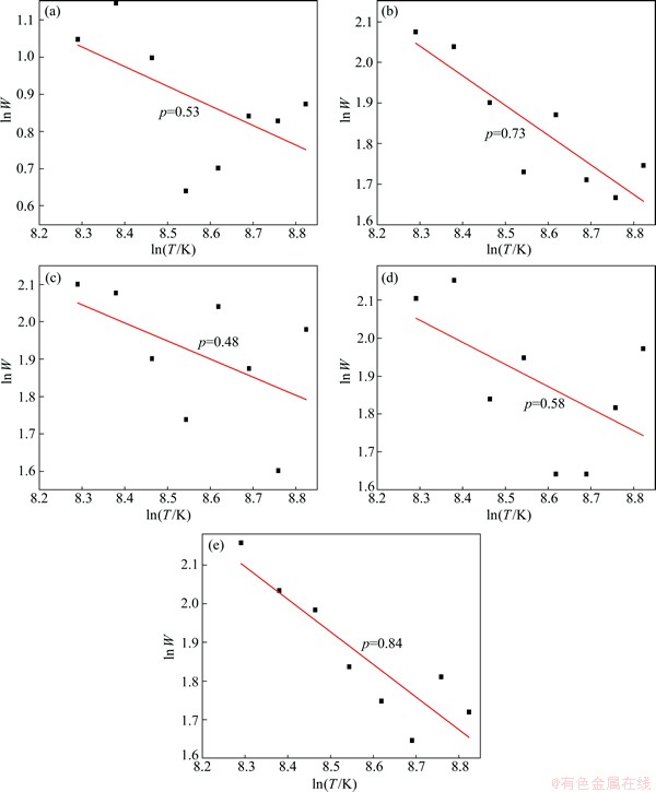
Fig. 4 ln W vs ln T plots for composite NTC thick films with x=0.05 (a), x=0.1 (b), x=0.15 (c), x=0.2 (d) and x=0.25 (e)
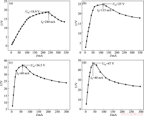
Fig. 5 Current�Cvoltage (I-U) characteristics of thick films at room temperature with x=0.05 (a), x=0.1 (b), x=0.15 (c) and x=0.2 (d)
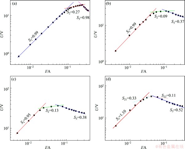
Fig. 6 Logarithmic I-U curves of thick films at room temperature with x=0.05 (a), x=0.1 (b), x=0.15 (c), and x=0.2 (d)
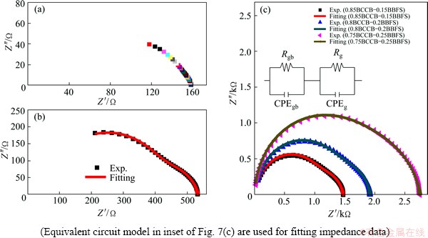
Fig. 7 Complex impedance spectroscopies of thick films at room temperature with x=0.05 (a), x=0.1 (b) and x=0.15-0.25 (c)
3.4 Impedance characteristics
Impedance spectroscopy is a powerful tool to analyze the conduction contribution for bulk materials [20-22]. Thus, it is also used to characterize the electrical properties in thick films. The complex impedance spectroscopies of the thick films at room temperature are plotted in Fig. 7. Where Z' and Z" denote the real and imaginary parts of impedance, respectively. For x=0.05, the Z"-Z' plot shows the incomplete circular due to lower room temperature resistance of the thick film. With the further increase of composition (x), a small arc at low frequencies and an incomplete large arc at high frequencies are observed in the Z"-Z' plots shown in Fig. 7(b). In Fig. 7(c), the Z"-Z' plots for the compositions with x=0.15, 0.2 and 0.25 exhibit more pronounced behavior and are clearly separated into two semicircular components. These characteristic electrical impedances can be well reproduced by an equivalent circuit with two CPE-R parallel circuits, as shown in the inset of Fig. 7(c), where CPE (Constant Phase Element) represents the non-ideal capacitance and R is the electrical resistance. The semicircle at the low frequency side corresponds to a contribution from circuit CPEgb-Rgb (Paralleling of CPEgb and Rgb), while that at the high frequency side corresponds to the contribution from circuit CPEg-Rg, where the subscripts ��gb�� and ��g�� represent the grain boundaries and grains, respectively. Hereinafter, the impedance responses in all samples are decomposed into two components and the fitted results are illustrated in Table 2. Interestingly, the grain response shows higher electrical resistance than the grain-boundary response. The obvious difference in the electrical response may be associated with the differences in the compositions and/or the microstructures for each of thick-film samples. When BBFS with high melting point is added into the low-melting BCCB material, the BBFS grain is firstly encaged by low-melting BCCB phase during the sintering process and then an approximate core-shell structure for the film grains may form in the composite films. According to the core-shell structures, the grain boundaries or the contacting interfaces between two grains are mainly composed of conductive BCCB phase with low melting point. Thus, the grains containing high-resistance BBFS phase show high electrical resistance, while the grain boundaries of thick films show low electrical resistance.
Table 2 Fitted parameters from grains and grain boundaries of thick films
The interior information obtained from grains may be better understood by comparing M" (Imaginary part of electric modulus) and Z" spectroscopic plots shown in Fig. 8. In Fig. 8, all the Z" spectra show one peak and one inflexion point but the M" spectra only show one peak. The single Z" inflexion point corresponds to the grain boundary relaxation behavior. The associated capacitance of the lower frequency M" peak is too large to be detected easily in the M" spectroscopic plot. At higher frequency region, the only peak in M" and Z" spectra is attributed to the contribution of grains. However, it is found that the peak position in M" and Z" spectra is not in the same frequency. This denotes that a weak composition difference in the grain surface occurs and the grains should be further divided into two parts of grain shells (gs) and grain cores (gc). However, it is very difficult to distinguish between grain shells and grain cores by Z-view software due to the weak difference. A further investigation needs to be made in the future.
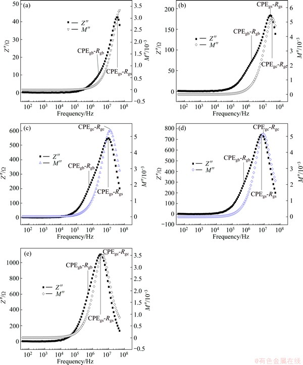
Fig. 8 Combined Z", M" spectroscopic plots of thick films at room temperature with x=0.05 (a), x=0.1 (b), x=0.15 (c), x=0.2 (d) and x=0.25 (e)
4 Conclusions
1) All thick-film compositions adopt the simple perovskite phases of cubic Ba0.5Bi0.5Fe0.9Sn0.1O3 and monoclinic .
2) With the increase of Ba0.5Bi0.5Fe0.9Sn0.1O3 content, the room temperature resistivities, activation energies and thermistor constants of the as-sintered films are in the ranges of 1.47-26.5 ����cm, 59-116 meV and 678-1345 K, respectively.
3) The conduction hopping type could be described by ES-VRH for the thick films with compositions x=0.05, 0.15 and 0.2, and that of the composite films with x=0.1 and 0.25 may be a transition from ES-VRH to NNH.
4) With the increase of the Ba0.5Bi0.5Fe0.9Sn0.1O3 content, the peak values of voltage show the increasing trend within the range of 18.9-47.0 V and the corresponding peak-voltage current decreases to 40 mA.
5) The thick films are composed of grains and grain boundaries and the electrical resistance of grains are larger than that of grains boundaries at various compositions.
References
[1] Macklen E D. Thermistor [M]. Ayr, Scotland: Electrochemical Publications Ltd., 1979.
[2] Prudenziati M. Handbook of thick film sensors [M]. Amsterdam, Holland: Elsevier, 1994.
[3] Jagtap S, Rane S, Gosavi S, Amalnerkar D. Study on I-V characteristics of lead free NTC thick film thermistor for self-heating application [J]. Microelectronic Engineering, 2011, 88(1): 82-86.
[4] Karanth S, Sumesh M A, Shobha V, Shanbhogue H G, Nagendra C L. Infrared detectors based on thin film thermistor of ternary Mn-Ni-Co-O on micro-machined thermal isolation structure [J]. Sensors and Actuators A, 2009, 153(1): 69-75.
[5] Schmidt R, Brinkman A W. Electrical properties of screen-printed NiMn2O4+�� [J]. Journal of the European Ceramic Society, 2005, 25(12): 3027-3031.
[6] Ryu J, Kim K Y, Choi J J, Hahn B D, Yoon W H, Lee B K, Park D S, Park C. Highly dense and nanograined NiMn2O4 negative temperature coefficient thermistor thick films fabricated by aerosol-deposition [J]. Journal of the American Ceramic Society, 2009, 92(12): 3084-3087.
[7] Schmidt R, Stiegelschmitt A, Roosen A, Brinkman A W. Screen printing of co-precipitated NiMn2O4+�� for production of NTCR thermistors [J]. Journal of the European Ceramic Society, 2003, 23(10): 1549-1558.
[8] Kang J E, Ryu J, Han G, Choi J J, Yoon W H, Hahn B D, Kim J W, Ahn C W, Choi J H, Park D S. LaNiO3 conducting particle dispersed NiMn2O4 nanocomposite NTC thermistor thick films by aerosol deposition [J]. Journal of Alloys and Compounds, 2012, 534: 70-73.
[9] Kanade S A, PURI V. Electrical properties of thick-film NTC thermistor composed of Ni0.8Co0.2Mn2O4 ceramic: Effect of inorganic oxide binder [J]. Materials Research Bulletin, 2008, 43(4): 819-824.
[10] JADHAV R, KULKARNI D, PURI V. Structural and electrical properties of fritless Ni(1-x)CuxMn2O4 (0��x��1) thick film NTC ceramic [J]. Journal of Materials Science: Materials in Electronics, 2010, 21(5): 503-508.
[11] KANADE S A, PURI V. Properties of thick film Ni0.6Co0.4FeyMn2-yO4: (0��y��0.5) NTC ceramic [J]. Journal of Alloys and Compounds, 2009, 475(1-2): 352-355.
[12] ALEKSIC O S, NIKOLIC M V, LUKOVIC M D, NIKOLIC N, RADOJCIC B M, RADOVANOVIC M, DJURIC Z, MITRIC M, NIKOLIC P M. Preparation and characterization of Cu and Zn modified nickel manganite NTC powders and thick film thermistors [J]. Materials Science and Engineering B, 2013, 178(3): 202-210.
[13] Liang Sen, Zhang Xiao, Bai Yu, Han Zhi-hai, Yang Jian-feng. Study on the preparation and electrical properties of NTC thick film thermistor deposited by supersonic atmospheric plasma spraying [J]. Applied Surface Science, 2011, 257(23): 9825-9829.
[14] Jagtap S, Rane S, Gosavi S, Amalnerkar D. Preparation, characterization and electrical properties of spinel-type environment friendly thick film NTC thermistors [J]. Journal of the European Ceramic Society, 2008, 28(13): 2501-2507.
[15] JAGTAP S, RANE S, GOSAVI S, AMALNERKAR D. Low temperature synthesis and characterization of NTC powder and its ��lead free�� thick film thermistors [J]. Microelectronic Engineering, 2010, 87(2): 104-107.
[16] Jagtap S, Rane S, Aiyer R, Gosavi S, Amalnerkar D. Study of microstructure, impedance and dc electrical properties of RuO2�Cspinel based screen printed ��green�� NTC thermistor [J]. Current Applied Physics, 2010, 10(4): 1156-1163.
[17] Yuan Chang-lai, Luo Ying, Zhou Xiu-juan, Zhou Chang-rong, Yang Yun, Liu Xin-yu. Microstructures and electrical properties of Ba1-xBixFe0.9Sn0.1O3 thermistor ceramics [J]. Advances in Applied Ceramics, 2013, 112(6): 322-330.
[18] YUAN Chang-lai, LIU Xin-yu, ZHOU Chang-rong, XU Ji-wen, LI Bo. Electrical properties of lead-free thick film NTC thermistors based on perovskite-type BaCoIIxCoIII2xBi1-3xO3 [J]. Materials Letters, 2011, 65(5): 836-839.
[19] Shklovskii B I, Efros A L. Electronic properties of doped semiconductors [M]//Berlin: Springer-Verlag, 1984.
[20] RAMESH S, JAMES RAJU K C, VISHNUVARDHAN REDDY C. Preparation and characterization of Ce1-xDyx-ySryO2-�� system [J]. Transactions of Nonferrous Metals Society of China, 2014, 24(2): 393-400.
[21] RAMESH S, RAJU K C J, REDDY C V. Properties of Al2O3-Sm2O3-CeO2 electrolyte [J]. Transactions of Nonferrous Metals Society of China, 2012, 22(6): 1486-1494.
[22] ZHANG D H, GUO H B, GONG S K. Impedance spectroscopy study of high-temperature oxidation of Gd2O3-Yb2O3 codoped zirconia thermal barrier coatings [J]. Transactions of Nonferrous Metals Society of China, 2011, 21(5): 1061-1067.
Ba0.5Bi0.5Fe0.9Sn0.1O3���Ӷ� ������Ĥ��ѧ���ܵ�Ӱ��
�� ��1��Ԭ����1���¹���1���� ��1���� ӱ2���ܲ���1
1. ���ֵ��ӿƼ���ѧ ���Ͽ�ѧ�빤��ѧԺ������ 541004��
2. ���ֵ��ӿƼ���ѧ ��ϢͨѶѧԺ������ 541004
ժ Ҫ������˿ӡ�������������Ʊ����е����µ����ʡ��������������ĸ��¶�ϵ�� / Ba0.5Bi0.5Fe0.9Sn0.1O3����������Ĥ���������ֶ��ñ�����ʱ��2400���迹�����Ƕ�������Ĥ�ĵ�ѧ���ܽ��б������������������Ba0.5Bi0.5Fe0.9Sn0.1O3������0.05������0.25����Ĥ�����µ����ʡ����������ͷ�ֵ��ѹ�����������ҷֱ���1.47~26.5 ����cm��678~1345 K��18.9~47.0V��Χ�ڣ���Ĥ��ֵ��ѹ��Ӧ�ĵ���Ҳ���������Ҵ���40~240 mA��Χ���迹�ײ��Ա�������Щ������Ĥ���ֳ������������ʵ�ѧ�ṹ��Ϊ���ɸ���̬�ľ����ͽϵ͵���̬�ľ������ɡ��ɴ˿�֪����������Ba0.5Bi0.5Fe0.9Sn0.1O3������������Ϊ��Ҳ���˵�������.
�ؼ��ʣ����¶�ϵ��������Ĥ����Ba0.5Bi0.5Fe0.9Sn0.1O3����ѧ����
(Edited by Mu-lan QIN)
Foundation item: Projects (51102055, 51462005) supported by the National Natural Science Foundation of China
Corresponding author: Chang-lai YUAN; Tel: +86-773-2291434; Fax: +86-773-2295903; E-mail: Yclguet@yahoo.com
DOI: 10.1016/S1003-6326(15)64050-X
Abstract: Thick-film thermistor with negative temperature coefficient (NTC), low room-temperature resistivity and modest thermistor constant was screen-printed on the alumina substrate by the combination of with Ba0.5Bi0.5Fe0.9Sn0.1O3. The electrical properties of the thick films were characterized by a digital multimeter, a Keithley 2400 and an impedance analyzer. The results show that with the Ba0.5Bi0.5Fe0.9Sn0.1O3 content increasing from 0.05 to 0.25, the values of room-temperature resistivity, thermistor constant and peak voltage of the thick films increases and are in the ranges of 1.47-26.5 ����cm, 678-1345 K and 18.9-47.0 V, respectively. The corresponding current at the peak voltage of the thick films decreases and is in the range of 40-240 mA. The impedance spectroscopy measurement demonstrates that the as-prepared thick films show the abnormal electrical heterogeneous microstructure, consisting of high-resistive grains and less resistive grain boundary regions. It can be concluded that the addition of Ba0.5Bi0.5Fe0.9Sn0.1O3 into improves the thermistor behavior and but also deteriorates the current characteristics.
