
Article ID: 1003-6326(2005)03-0519-05
Surface morphology and photoluminescence properties of ZnO thin films obtained by PLD
FAN Xi-mei(��ϣ÷)1, 2, LIAN Jian-she(������)1,
GUO Zuo-xing(������)1, JIANG Qing(�� ��)1
(1. Key Lab of Automobile Materials, Ministry of Education,
College of Materials Science and Engineering, Jilin University, Changchun 130025, China;
2. College of Materials Engineering, Southwest Jiaotong University,
Chengdu 610031, China)
Abstract:
ZnO thin films on Si(111) substrate were deposited by laser ablation of Zn target in oxygen reactive atmosphere, Nd-YAG laser with wavelength of 1064nm was used as laser source. XRD and FESEM microscopy were applied to characterize the structure and surface morphology of the deposited ZnO films. The optical properties of the ZnO thin films were characterized by photoluminescence. The UV and deep level (yellow-green) light were observed from the films. The UV light is the intrinsic property and deep level light is attributed to the existence of antisite defects (OZn). The intensity of UV and deep level light depends strongly on the surface morphology and is explained by the surface roughness of ZnO film. A strongly UV emission can be obtained from ZnO film with surface roughness in nanometer range.
Key words:
ZnO; pulsed laser deposition; UV photoluminescence; film CLC number: TN304.2 ; ; ; ; ; ; ; ; ; ; ; ; ;Document code: A;
1 INTRODUCTION
One important advantage of ZnO is that it is a ��-�� semiconductor of wurtzite structure with a wide direct-band-gap of 3.3eV at room temperature[1]. The most unique property of ZnO is its large exciton binding energy of 60meV, which is much larger than those of GaN (24meV), ZnSe (19meV) and ZnS (39meV)[2]. Because of this large binding energy, the exciton is stable at room temperature even in bulk crystals. Owing to these properties, ZnO is considered a promising material for light-emitting devices and semiconductor lasers with low thresholds in the UV region, such as light-emitting diodes and laser diodes[3-5]. ZnO films with high intensity emission have been deposited by using several growth techniques, such as metal-organic chemical vapour deposition (MOCVD)[6], molecular beam epitaxy (MBE)[7], sol-gel deposition[8], rf magnetron sputtering[9] and reactive DC sputtering[10], oxidation of metal zinc film[11], pulse laser deposition (PLD)[12]. Pulse laser deposition (PLD) technique is more useful in obtaining high quality thin films of metal oxide materials compared with other techniques, because of its advantage of simple hardware, atomic-layer control obtained by adjusting the laser energy density, the pulse duration and repetition rate. For these practical reasons, PLD technique has been widely applied for the formation of the high quality thin films.
In consideration of low-cost preparation of ZnO film, in the present work, we applied a very common laser apparatus (Nd-YAG laser of 1064nm) and a Zn target (which is much cheaper than ZnO target) to deposit ZnO thin films at different substrate temperatures by laser (wavelength of 1064nm) ablation of Zn target in oxygen active atmosphere. The influence of temperature on the surface morphology and photoluminescence property was studied.
2 EXPERIMENTAL
Si(111) substrates were used as the underlay. Si substrates were rinsed three times in acetone with ultrasonic vibration for 15min each time, and then rinsed in ethanol for 15min before it was put into the deposition chamber. The experiments were performed in a deposition system. Before deposition, the vacuum chamber of the deposition system was evacuated by turbo-molecular pump down to 5��10-4Pa and then filled with oxygen (99.99% purity ) at a working pressure. The laser energy density was measured to be about 31J/cm2. Zn (99.99% purity) targets were ablated by a Nd-YAG laser (wavelength of 1064nm, with pulse duration of 100ns, frequency of 10Hz). The target-substrate distance was kept at 2.5cm. The deposition time of 20min was maintained. The film thickness measured by the cross section image of SEM was 0.8-1.3��m, which depended on the substrate temperature. In the present experiment, the heater block temperature was considered the substrate temperature. ZnO thin films were deposited at the substrate temperature of 300, 400, 500�� with oxygen pressure of 11Pa. After deposition, the film crystal structure was investigated by X-ray diffraction (XRD, Rigaku Dymax) with a Cu target and a mono-chronmator at 50kV and 300mA. FESEM (JSM-6700F) was used to characterize the surface morphology of the film. The optical properties of the ZnO thin films were characterized by photoluminescence with an Ar ion laser as a light source using an excitation wavelength of 325nm. All spectra were measured at room temperature.
3 RESULTS AND DISCUSSION
3.1 Structure of ZnO film
Fig.1 shows the XRD patterns of the ZnO thin films on Si(111) substrate obtained by laser ablation of Zn target in oxygen reactive atmosphere at different substrate temperatures (300, 400 and 500��) with a fixed oxygen pressure of 11Pa. Three main diffraction peaks of ZnO thin films appear at 2��=31.81��, 34.46�� and 36.27��, which are corresponding to the (100) plane, (002) plane and (101) plane of ZnO thin films, respectively. In order to evaluate the average grain size of the films, we adopted the Scherrer formula using the full width at half maximum (FWHM) value of the XRD diffraction peaks. The Scherrer formula is d=0.94��/(Bcos��), where d, ��, ��, and B are the mean grain size, the X-ray wavelength of 0.154�@, Bragg diffraction angle, and the FWHM of the diffraction peak of ZnO film, respectively. The calculated mean grain sizes are 14.1, 16.5 and 20.2nm for the ZnO films deposited at the substrate temperature of 300, 400 and 500��, respectively. That is, nanocrystalline grained ZnO films were obtained. It is observed that the films obtained at the substrate temperature of 300�� and 400�� have random polycrystalline structure without preferred orientation. However, when the substrate temperature is increased to 500��, only two diffraction peaks of (002) and (101) exist and (002) peak has the maximum diffraction intensity. This shows that a structure with main (002) orientation or c-axis growth forms at substrate temperature of 500��.
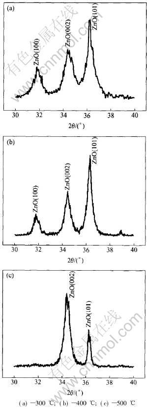
Fig.1 XRD patterns of ZnO thin films on Si(111) grown by PLD at different substrate temperatures
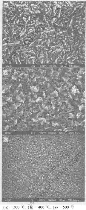
Fig.2 FESEM micrographs of ZnO thin films on Si(111) grown by PLD at different substrate temperatures
Fig.2 shows the FESEM micrographs of the ZnO films obtained at different substrate temperatures corresponding to Fig.1. It is found that there is great difference in surface morphology among the ZnO films deposited at different substrate temperatures. ZnO film deposited at 300�� (Fig.2(a)) has a petal-like surface morphology and a large surface roughness. The size of most clusters(petals) is 200-300nm. Both the surface roughness and the cluster size (100-250nm) of ZnO film deposited at 400�� (Fig.2(b)) are somewhat less than those deposited at 300��. In contrast, the ZnO film deposited at 500�� has very small clusters (40-60nm) and surface roughness (Fig.2(c)).
From the above results, it is known that the surface of ZnO film with (002) preferred orientation is relatively smooth. During PLD, the kinetics of atomic arrangement is mainly influenced by the substrate temperature and the energy of deposition atoms. It was reported that the (002) orientation had the lowest surface energy among these orientations[13]. Therefore, at a relatively high temperature, atoms on the surface have high mobility. There should be enough time for adatoms to move on surface to look for the lowest energy sites before the adatoms are covered by the next layer of atoms. The homogeneous growth results in a smooth surface structure. However, at relative low growth temperature (for example, 300��), random growth results in more rough surface structure.
3.2 Photoluminescence characteristics of film
Fig.3 shows the room temperature photoluminescence (PL) spectra obtained from the ZnO thin films on Si(111) substrate deposited at different substrate temperatures (300, 400 and 500��) with a fixed oxygen pressure of 11Pa. The PL spectra of ZnO film consist of a UV emission centering about 378-394nm and a yellow-green emission centering about 515-525nm. It can be seen that the intensity of narrow UV emission peak increases markedly with the increase of the substrate temperature in the range of 300-500��. As to the yellow-green emission of PL spectra, the main center of these peaks is about 518nm, or 2.386eV.
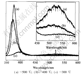
Fig.3 Room temperature (298K) PL spectra of ZnO thin films on Si(111) grown by PLD at different substrate temperatures
FAN et al[14] had calculated the energy levels of the intrinsic defects in ZnO by applying the full-potential linear muffin-tin orbital method. The calculated energy level for the UV emission is 3.18eV, and the calculated energy interval from the bottom of the conduction band to the antisite oxygen OZn is 2.38eV. Therefore, the experimental UV emission at 375-395nm (or 3.27-3.14eV) of PL spectra of ZnO films approximates the theoretically calculated value of 3.18eV of UV emission, and the deep level emission observed in our experiment (2.39eV) is in coincidence with the calculated energy interval of electronics transition from the bottom of the conduction band to the antisite oxygen OZn defect. That is, the UV emission is the intrinsic property of ZnO film, and the deep level emission of yellow-green light is attributed to antisite oxygen OZn defects[15].
It is observed from Fig.3 that both the intensities of UV emission and deep level emission of ZnO film depend strongly on the substrate temperature during the deposition. This can be explained by the cluster size or surface roughness of ZnO film formed at different substrate temperatures(see Fig.2). Fig.4 shows the plot of both the UV peak and deep level peak intensities varying with the average cluster size (the surface roughness can be considered to be the same or similar level as the cluster size). It is observed that the intensity decreases as the average cluster size increases. For ZnO film deposited at 500��, an even surface with the average cluster size or roughness less than 50nm is obtained, the UV emission with wavelength about 385nm (or deep level emission with wavelength about 518nm) of PL spectra from the ZnO crystals on top surface and on valley surface have the similar phases. The interference enhancement of light with similar phases can be achieved and a strong UV (or deep level) emission is obtained from the ZnO film deposited at 500��. For the case that ZnO film deposited at 300��, the phase difference between the light emitted from the valleys surface and the light emitted from the top surface approaches to half wavelength (about 190nm for the UV light and 260nm for the deep level emission light). The weakening of light through the interference of them is possible and low intensity emission of UV and deep level light is observed from ZnO film deposited at this temperature. The interference strengthening of light is usually
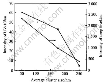
Fig.4 Variation of UV and deep level intensity with surface cluster size of ZnO film
observed from the nano-crystalline material surface obtained from electro-deposition method, for example, a mirror-like surface was observed from the electroplating nano-crystalline Ni-Fe with nanometer sized surface roughness (from 22.7nm to 64.9nm)[16].
4 CONCLUSIONS
ZnO film on Si substrate was obtained by ablation of Zn target in oxygen atmosphere, with a Nd-YAG laser of 1064nm wavelength as the pulse laser source. The influences of the substrate temperature on the structure and optical properties of ZnO film were studied.
1) The ZnO films obtained at the substrate temperatures of 300�� and 400�� have random polycrystalline structure and sub-micrometer rough surface, and the ZnO film formed at the substrate temperature 500�� has mainly (002) texture and even surface with nanometer roughness.
2) All samples show UV emissions and deep level emissions (yellow-green light) in PL spectra. The UV emission is the intrinsic property of ZnO film and the deep level emission is attributed to the electron transitions from the bottom of the conduction band to the antisite oxygen OZn defects level.
3) The intensity of PL light increases with the increasing of the deposited substrate temperature of ZnO films. This is explained by the surface roughness or cluster size of ZnO film. ZnO film which has nanometer sized surface roughness emits intense UV light due to the interference strengthening of light with similar phases.
Acknowledgements
The authors would like to thank Prof. Y.C.Liu for many supports at optical experiment in Northeast Normal University.
REFERENCES
[1]Berger L I. Semiconductor Materials[M]. New York: CRC Press, 1997.
[2]Yamamoto A S, Miyajima K S, Goto T. Biexciton luminescence in high-quality ZnO epitaxial thin films[J]. J Appl Phys, 2001, 90(10): 4973-4976.
[3]Zu P, Tang Z K, Wong G K L. Ultraviolet spontaneous and stimulated emissions from ZnO microcrystallite thin films at room temperature[J]. Solid State Commun, 1997, 103(8): 459-463.
[4]Hayamizu S, Tabata H, Tanaka H. Preparation of crystallized zinc oxide films on amorphous glass substrates by pulsed laser deposition[J]. J Appl Phys, 1996, 80(2): 787-791.
[5]Sun X W, Kwok H S. Optical properties of epitaxially grown zinc oxide films on sapphire by pulsed laser deposition[J]. J Appl Phys, 1999, 86(1): 408-411.
[6]Kashiwaba Y, Sugawara K, Haga K. Characteristics of c-axis oriented large grain ZnO films prepared by low pressure MO-CVD method[J]. Thin Solid Films, 2002, 411(1): 87-90.
[7]Ko H J, Chen Y F, Zhu Z. Photoluminescence properties of ZnO epilayers grown on CaF2(111) by plasma assisted molecular beam epitaxy[J]. Appl Phys Lett, 2000, 76(26): 1905-1907.
[8]Natsume Y, Sakata H. Zinc oxide films prepared by sol-gel spin-coating[J]. Thin Solid Films, 2000, 372(1-2): 30-36.
[9]Kim K K, Song J H, Jung H J, et al. The grain size effects on the photoluminescence of ZnO/��-Al2O3 grown by radio-frequency magnetron sputtering[J]. J Appl Phys, 2000, 87(8): 3573-3575.
[10]ZHANG G B, SHI C S, HAN Z F. Photoluminescent properties of ZnO films deposited on Si substrates[J]. Chin Phys Lett, 2001, 18(3): 441-442.
[11]CHEN X J, LIU Y C, MA J G. High-quality ZnO thin films prepared by two-step thermal oxidation of the metallic Zn[J]. Journal of Crystal Growth, 2002, 240(3-4): 467-472.
[12]Jin B J, Im S, Lee S Y. Violet and UV luminescence emitted from ZnO thin films grown on sapphire by pulsed laser deposition[J]. Thin Solid Films, 2000, 366(1-2): 107-110.
[13]Bae S H, Lee S Y, Kim H Y. Comparison of the optical properties of ZnO thin films grown on various substrates by pulsed laser deposition[J]. Applied Surface Science, 2000, 168(1-4): 332-334.
[14]FAN X M, LIAN J S, GUO Z X, et al. Microstructure and photoluminescence properties of ZnO thin films grown by PLD on Si(111) substrates [J]. Applied Surface Science, 2005, 239: 176-181.
[15]Lin B, Fu Z, Jia Y. Green luminescent center in undoped zinc oxide films deposited on silicon substrates[J]. Appl Phys Lett, 2001, 79(7): 943-945.
[16]Czerwinski F, Szpunar J A. Structural and magnetic characterization of nano-crystalline Ni-20%Fe permalloy films[J]. Journal of Materials Science, 2000, 11(1-2): 243-251.
(Edited by YUAN Sai-qian)
Foundation item: Project (2004CB619301) supported by The National Basic Research Program of China
Received date: 2004-12-09; Accepted date: 2005-04-08
Correspondence: LIAN Jian-she, Professor; Tel: +86-431-5095875; Fax: +86-431-5095876; E-mail: lianjs@jlu.edu.cn
