

Simulation and prediction in laser bending of silicon sheet
WANG Xu-yue, XU Wei-xing, XU Wen-ji, HU Ya-feng, LIANG Yan-de, WANG Lian-ji
Key Laboratory for Precision and Non-traditional Machining Technology of the Ministry of Education,
Dalian University of Technology, Dalian 116024, China
Received 21 April 2010; accepted 10 September 2010
Abstract:
The laser bending of single-crystal silicon sheet (0.2 mm in thickness) was investigated with JK701 Nd:YAG laser. The models were developed to describe the beam characteristics of pulsed laser. In order to simulate the process of laser bending, the FEM software ANSYS was used to predict the heat temperature and stress-strain fields. The periodic transformation of temperature field and stress-strain distribution was analyzed during pulsed laser scanning silicon sheet. The results indicate that the mechanism of pulsed laser bending silicon is a hybrid mechanism in silicon bending, rather than a simple mechanism of TGM or BM. This work also gets silicon sheet bent after scanning 6 times with pulsed laser, and its bending angle is up to 6.5?. The simulation and prediction results reach well agreement with the verifying experiments.
Key words:
laser bending; silicon sheet; pulsed laser; simulation;
1 Introduction
Single-crystal silicon as major semiconductor materials is widely used in various fields. The reason lies not only on silicon having excellent electronic properties, but also good mechanical properties[1-5]. Plastic reshaping at room temperature, commonly used in metal processing, is not possible in the case of silicon reshaping because of its brittleness. Only when the temperature is over 790 K, the transition from brittle to ductile behavior is followed and the forming plastic deformation becomes easy at temperature higher than 920 K[5-6]. In micro-electro-mechanical systems (MEMS), three-dimensional microstructural elements of silicon are mainly prepared by anisotropic etching, so they are lying inside the wafer plane. But with its plastic reshape, the microstructure can be created outside the wafer. On the other hand, silicon forming needs furnace heating the whole wafer to the ductile temperature and mold or force rod[6-7]. Then the manufacture of mold and the heating methods could take more time, also the forming shapes were influenced most by these methods[8].
There are two mechanisms for laser bending, including the temperature gradient mechanism (TGM) and buckling mechanism (BM) that depends on the geometry and the physical properties of the target material properties. In the local laser treatment, the heat flux to the neighboring material is minimized and the beam can be applied through windows of glass[8-9].
The stress-strain and temperature changing in the process of laser bending are very complicated. With the help of numerical simulation, the bending process can be reproduced, including bending direction and change of temperature, stress-strain and angle during scanning [10-12]. In this work, the meshing of elements is optimized and a physical model of pulsed laser is built, according to its character in optical space-time. The numerical simulation is based on the performance of thermo-physical and thermo-dynamic parameter on (110) face of single-crystal silicon. This research gets the characteristics of stress-strain and temperature field, and analyzes the laser bending deformation mechanism.
2 Modeling of laser beam
2.1 Laser beam model
Laser beam can be divided into longitudinal mode and transverse mode, according to different oscillation modes in the resonator. Fundamental mode is the basic mode of transverse mode. Its optical field distribution is not only axial symmetry, but also rotational symmetry.
The intensity of beam wave is proportional to its electric vector amplitude. A laser beam spreading along the z-direction is expressed as[10]:
![]() ���� ��(1)
���� ��(1)
where P is the laser power; w(z) is the spot radius at z cross-section.
The intensity distribution of basic mode can be described by the law of smooth decline from center to outside in arbitrary cross-section. The spot radius w(z) is defined as beam intensity drop to the 1/e2 times that of the center. It contains 86.5% of the total beam energy and the intensity of center is 2P/[��w2(z)].
2.2 Pulsed laser models both in space and time
The characteristic of pulsed laser is that the laser beam is exported continuously as an optical pulse in a certain cycle. In each cycle, it is accompanied with a laser process and a spacing process. In a laser pulse, the output beam energy is uneven and there exist two obvious processes, the declining stage and the rising stage (see Fig.1). For a beam pulse[9]:
 ���� (2)
where Ep is the beam pulse energy and tp is the pulse duration. And there is
 (3)
(3)
Then, we have
 (4)
(4)
where I0(t) is the center spot beam intensity at t moment. Fitting Eq.(1) and Eq.(4) together, the temporal and spatial distribution formula within the laser beam pulse can be obtained as follows:
 (5)
(5)
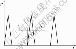
Fig.1 Model in time series of pulsed laser
It is evident that the nearer the spot center is, the greater the beam intensity is and the faster the spot is warmed during the laser irradiation to the workpiece surface. This should be paid attention to modeling and meshing.
2.3 Modeling
The computer simulation of laser bending is a complicated process because it involves many variables such as heat flux of the laser beam, temperature distribution in the elements, factor changes in material properties and influence of thermal strains on the deformations. The process generally includes three distinct components: the modeling of laser beam, the transfer of heat from the laser beam to the plate and the response of the plate. Finite element analysis software ANSYS has powerful nonlinear analysis capabilities that enable multiple physical field mutual coupling with the simulation process based on ANSYS Parametric Design Language (APDL). In order to calculate the thermal structure coupled field with large plastic deformation, an indirect coupled field analysis was performed.
Firstly, the geometric modeling is built and element SOLID70 (eight-node 3-D thermal solid with thermal conduction, convection and material non-linearity) for thermal analysis is chosen. Then meshing of the model is carried out and is optimized according to the initial temperature field. After that, the thermo-physical parameters of silicon, load equivalent heat flow calculated by the spatial and temporal characteristics of pulsed laser beam intensity are input, and temporal and spatial temperature fields are simulated.
In the structural analysis, the structure element SOLID45 (eight-node 3-D solid with extra shape functions, large elastoplastic deformation, and geometric and material non-linearity) will be used instead of SOLID70. After inputting the thermodynamic parameters, the temperature field will be reloaded as force for simulating the process of stress and strain in laser bending.
3 Temperature field simulation and analysis
3.1 Single pulse processing
As shown in Fig.2, for the simulation of laser bending silicon, the geometric model dimensions of 2 mm��10 mm��100 ��m, single-pulse laser energy of 0.04 J, pulse width of 2 ms, frequency of 30 Hz, spot radius of 0.4 mm, and scanning speed of 100 mm/min are selected. The pulsed laser beam scans between A and B, where points P1, P2, P3 are on the scanning line and points P4, P5, P6 are the corresponding points below the scanning line.
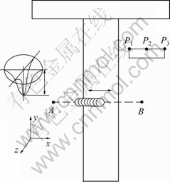
Fig.2 Laser scanning path
Figure 3 shows the distribution of temperature along the scanning path at laser pulsed point P2. It is clear that for each beam pulse, the effect point is accompanied by a rapid warming and cooling process. In this whole process, the hot spot area is small and does not exceed the basic beam spot, which is consistent with the experimental phenomenon.
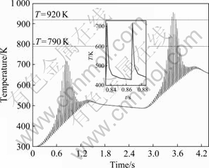
Fig.3 Transient temperature distribution along scanning path at laser pulsed point P2
3.2 Multiple scanning characteristics
Figure 4 shows the temperature change of point P2, during the previous twice laser scanning. The temperature of point P2 is periodically jumping, with the laser beam moving. The more the spot center near the point P2 is, the greater the temperature fluctuations is; when it affects the point P2, the temperature reaches the highest. With the subsequent away from the spot, the jumping is decreased, but the temperature of point P2 relatively rises after each pulse.
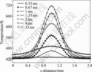
Fig.4 Temperature distribution at point P2
3.3 Laser bending mechanism
Laser-induced bending with continuous wave (CW) occurs with three principal mechanisms, the temperature gradient mechanism (TGM), the buckling mechanism (BM) and the upsetting mechanism (UM)[13-15]. The principle mechanism activated is mainly dependent on the laser processing parameters, and the workpiece thickness and the material properties.
Figure 5 shows the temperature distribution on the cross section at the laser pulsed point P2 with a pulse cycle at the time of 0.33, 1, 2 ms. Temperature gradient exists obviously along the thickness direction under the pulse laser action. This is typically the TGM. But, when a pulse completes and the next one does not come at the heat diffusion process stage, there is no apparent temperature gradient along the thickness direction. It is attributed to BM. Therefore, the mechanism of pulsed laser bending of silicon is not a simple principle of the TGM or BM. But, the hybrid results of the two bending mechanism act together.
4 Stress-strain simulation and prediction
Based on the thermo-dynamic properties of (110) plane of the single-crystal silicon, the simulation results of temperature field were reloaded on the model for the stress-strain simulation[16-20]. The process of the pulse laser induced a dramatic complexity change on stress and strain for its violent jumping of the temperature.
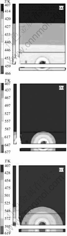
Fig.5 Transient temperature distribution of section at laser pulsed point P2: (a) t=0.33 ms; (b) t=1 ms; (c) t=2 ms
Figure 6 shows the thermal stress and strain distribution along y-direction in a pulse cycle, perpendicular to the scanning path at point P2, when the pulse laser first passes the point P2. In comparison with Fig.3, the thermal stress of the hot spot area keeps increasing with increasing the temperature. When the optical pulse works for 1.33 ms in a cycle, the thermal stress comes to the highest of 740 MPa. The temperature at the spot center is 720 K which is below the plastic temperature. So the pulsed laser induces no plastic deformation, and only lead to a certain degree of elastic fluctuation, and the brittle feature of silicon appears still. After that, the thermal stress and strain begin decreasing with the increase of temperature, and reduce to zero at the time about 33 ms.
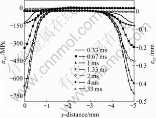
Fig.6 Stress-strain distribution along y-direction at laser pulsed point P2
Figure 7 shows the displacement related bending angle of the free-end at the previous two scans. When the optical pulses act on the workpiece, the temperature increases, leading to higher temperature gradient and anti-bending at the action area resulting from the thermal stress. Then the free-end begins to have the displacement, but the following gradual spread of the temperature makes temperature gradient reduce and the free-end starts rebound. Compared with the previous two scannings, it can be seen when the laser first passes point P2, the temperature of the work area is below the plastic temperature and the free-end rebounds to the original position, which belongs to elastic deformation; when the second laser passes point P2, the temperature of the work area is higher than 800 K, the final position of the free-end cannot return to the original state at the plastic situation, then the bending toward the laser beam irradiation belongs to plastic deformation.
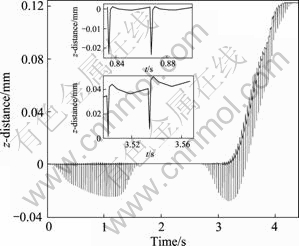
Fig.7 Displacements of free-end
Therefore, we can describe the pulsed laser bending of silicon as follows: every laser pulse causes free-end fluctuating when the temperature of the work area is lower than that of the plastic point, and all the fluctuations are elastic vibration; when temperature is higher than that of plastic point, the pulsed laser causes plastic deformation too. The prediction of bending angle is up to 6.4?.
5 Verifying experiments
Experiments for pulsed laser bending were performed with the single-sided polished (110) wafer of silicon. Nd:YAG laser (1.064 ��m) was used in welding mode with a single pulse energy of 0.04 J, pulse width of 2 ms, output frequency of 30 Hz, defocusing amount of 16 mm (spot radius of 0.4 mm). At the same time, the test samples were prepared to 5 mm-width, 10 mm- length and 200 ��m-thickness.
Figure 8 shows the finally bending effects after scanning 6 times along the path with the speed of 100 mm/min. The bent angle is up to 6.5?. Figure 9 shows the records of the experiments at each scan and the corresponding numerical simulation results. From the second scan, the silicon sheet is obviously curve bent, and bending angle increases nearly linearly with scanning times. The bending angle apart from the second scan is a bit higher than the experimental bending angle. All experiments are consistent with the simulation and prediction results.
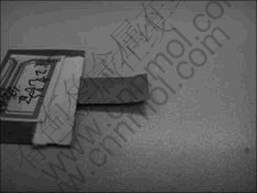
Fig.8 Bended sample after 6 scans
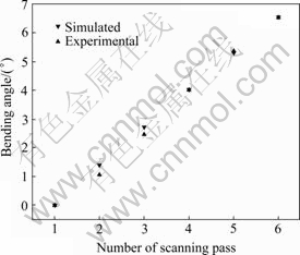
Fig.9 Relationship between scanning pass and bending angle
6 Conclusions
1) The scanning area is accompanied with dramatic heating and cooling process in each pulse acting cycle, and the temperature of the workpiece of scanning area increases. The temperature distribution on the cross sections indicates that the mechanism of the pulsed laser bending of silicon obeys a hybrid mechanism, rather than a simple mechanism of TGM or BM.
2) For brittle material, such as silicon, each optical pulse causes a front-back bending process in scanning area. If the temperature lowers the plastic point, this process belongs to elastic deformation and it does not produce bending effects. When the temperature is higher than plastic point, the bending is accompanied with plastic deformation and the final position departs from the original location. Since then, the silicon sheets are gradually bent along with the deformation fluctuations.
3) The bending experiment makes silicon bend clearly and the workpiece bending angle is 6.5? after 6 scans. Laser bending simulation and predictions reach well agreement with the experiments. The numerical simulation of laser bending is also suitable for other materials when bending temperature changes, considering the in thermo-physical and thermo- dynamics properties of material.
References
[1] PETERSEN K. E. Silicon as a mechanical material [J]. Proceedings of the IEEE, 1982, 70(5): 420-457.
[2] CUI Jian-feng, ZHAO Jing, FAN Zhong-wei, ZHAO Chun-hua, ZHANG Jing, NIU Gang, SHI Zhao-hui, PEI Bo, ZHANG Guo-xin, XUE Yan, BI Yong, QI Yan. Study on LD-pumped Nd:YAG laser cutter for silicon wafer [J]. Opt Precison Eng, 2006, 14(5): 829-834. (in Chinese)
[3] WU Dong-jiang, XU Yuan, WANG Xu-yue, KANG Ren-ke, SIMA Yuan, HU Li-zhong. Experimental and theoretical study on laser cleaning Al2O3 particle on silicon wafer surface [J]. Opt Precison Eng, 2006, 14(5): 764-770. (in Chinese)
[4] WANG Xu-yue, XU Wei-xing, SIMA Yuan, WU Dong-jiang, KANG Ren-ke, GUO Dong-ming. Evaluation of efficiency for silicon wafer cleaning by image processing [J]. Opt Precison Eng, 2007, 15(8): 1263-1268. (in Chinese)
[5] JOACHIM F, EVA G, ERHANRD J. Silicon as a plastic material [J]. J Micromech Microeng, 1999, 9: 305-312.
[6] EXNER H, L?SCHNER U. Contactless laser bending of silicon microstructures [C]// Proc of SPIE. Maspalomas, 2003, 5113: 383-392.
[7] WANG Xu-yue, WANG Jing-song, XU Wei-ji, CHENG Li-fang, WU Dong-jiang. Parameter prediction of bending of aluminum alloy sheet induced by laser prompt heating [J]. Opt Precision Eng, 2007, 15(6): 915-921. (in Chinese)
[8] YANG Chao-jun, ZHOU Jian-zhong, ZHANG Yong-kang, ZHANG Fang. Study on calculation of minimum laser energy of sheet metal deformation by laser shock forming [J]. Opt Precison Eng, 2006, 14(3): 396-401. (in Chinese)
[9] ZHANG X R, CHEN G. Numerical simulation of pulsed laser bending [J]. Journal of Applied Mechanics, 2002, 69: 254-260.
[10] LI J C. Laser diffraction and thermal calculation [M]. Beijing: Science Press, 2003: 220-222. (in Chinese)
[11] CHEN Yan-bin, LI Li-qun, LIN Shang-yang. The FEM simulation of the temperature field in laser forming [J]. Applied Laser, 2002, 22(2): 145-149. (in Chinese)
[12] XU X F, SONG K H. Phase change phenomena during high power laser-materials interaction [J]. Materials Science and Engineering A, 2000, 292(2): 162-168.
[13] CORRERA L, BENTINI G.G. Thermal profiles and thermal stresses introduced on silicon during scanning line shaped beam annealing [J]. J Appl Phys, 1983, 54(8): 4330-4337.
[14] SHEN H, SHI Y J, YAO Z Q. Numerical simulation of the laser forming of plates using two simultaneous scans [J]. Computational Materials Science, 2006, 37(3): 239-245.
[15] ZHANG X R, XU X F. High precision microscale bending by pulsed and CW lasers [J]. Journal of Manufacturing Science and Engineering, 2003, 125(3): 512-518.
[16] WIDMER A E, REHWALD W. Thermoplastic deformation of silicon wafers [J]. J Eelectrochem Soc, 1986, 133(11): 2403-2409.
[17] YI T, KIM C J. Measurement of mechanical properties for MEMS materials [J]. Meas Sci Technol, 1999, 10: 706-716.
[18] NAKAO S, ANDO T, SHIKIDA M, SATO K. Mechanical properties of a micron-sized SCS film in a high-temperature environment [J]. J Micromech Microeng, 2006, 16: 715-720.
[19] WALTERS D S, SPEARING S M. On the flexural creep of single-crystal silicon [J]. Scripta Mater, 2000, 42(8): 769-774.
[20] MINOR A M, LILLEODDEN E T, JIN M, STACH E A, CHARZAN D C, MORRIS J W Jr. Room temperature dislocation plasticity in silicon [J]. Philosophical Magazine, 2005, 85(2-3): 323-330.
(Edited by YANG Hua)
Foundation item: Projects (50975041, 50775019) supported by the National Natural Science Foundation of China; Projects (20062181, 2008S054) supported by Liaoning Province��s Government Science Fund, China
Corresponding author: XU Wen-ji; Tel: +86-411-84708422; E-mail: wenjixu@dlut.edu.cn
