
����BeO����Ķ����ս�
��С��1, 2�����ճ�2������Ⱥ2����־��2
(1. ���ϴ�ѧ ұ���뻷��ѧԺ������ ��ɳ��410083��
2. ���ϴ�ѧ ���Ͽ�ѧ�빤��ѧԺ������ ��ɳ��410083)
ժ Ҫ��
�ľ������������ö����ս᷽���о�����BeO������սᡣ����2�������ս�ʵ��ȷ��ÿ���ս���¶ȷ�Χ֮���о�����BeO����Ķ����սṤ�գ�ͨ��ɨ�����������ͼ����������о��ս����������֯�ṹ�ı仯�����ü�����Dz��Բ��ϵ��ȵ��ʣ�����������BeO����Ķ����ս���ơ��о������������1�����ս��¶�(t1)��ΧΪ1 450 ���C.rsity, Changsha 410083, Chi8na;, Central South t1��1 500 �棻��2�����ս��¶�(t2)��ΧΪ1 300 ���t2��1 400 �棻�Ϻ��ʵĶ����սṤ��Ϊ��(1 450 �棬1 min)+(1 400 �棬25 h)���ù����������մɵ�����֯�ṹ�Ͼ��ȣ����ܶȺ��ȵ��ʾ��ϸߣ��ֱ�Ϊ96.6%��237 W/(m��K)��������BeO����Ķ����ս�����У�������ɢ������ɢ���������ܻ��Ļ�������Ҫ���á�
�ؼ��ʣ�
�����ս�������BeO���ս�������ȵ�����
��ͼ����ţ�TF123 ���ױ�־�룺A ���±�ţ�1672-7207(2014)04-1043-09
Two-step sintering of BeO nanopowder
WANG Xiaofeng1, 2, WANG Richu2, PENG Chaoqun2, WANG Zhiyong2
(1. School of Metallurgy and Environment, Central South University, Changsha 410083, China;
2. School of Materials Science and Engineering, Central South University, Changsha 410083, China)
Abstract: In order to control the grain growth during the final stage of sintering, two-step sintering method was employed to consolidate BeO nanoparticles. Experiments were conducted to determine the appropriate temperatures for each step, and then the two-step sintering process of BeO was studied. The two-step sintering regimes were also analyzed. The results show that temperature ranges for the first step sintering (t1) and the second step sintering (t2) are 1 450-1 500 �� and 1 300-1 400 ��, respectively, the optimized two-step sintering process is (1 450 ��, 1 min)+(1 400 ��, 25 h), BeO ceramic with well-proportioned microstructure and comfortable relative density (96.6%) is achieved and its thermal conductivity is 237 W/(m��K), and the sintering mechanism of nano-BeO is grain boundary diffusion and volume diffusion.
Key words: two-step sintering; nano-BeO; sintering mechanism; thermal conductivity
BeO�մ�������и��ȵ��ʡ������Ľ�����ܺ����õĹ�����Ӧ�Եȵ��ӷ�װ���ԣ�һֱ���Ʊ��ߵ���Ԫ�����������մɲ���[1-3]������BeO���۵�ߴ�(2 570��20) ��[1]��������ͨ�������Ʊ�BeO�մɵ��ս��¶Ⱥܸߣ����Խ��ѻ�ø����ܵ���������IJ���[1, 3]����ˣ�Ϊ�˽����ս��¶ȣ�Wang��[4]����������BeO�������Ʊ��մɲ��ϡ����ǣ��������ڳ����ս�����м����������γɽ϶�Ŀ������Ի�õIJ��ϵ�����ܶ�Ҳ���ߣ��ȵ��ʽ�Ϊ186.6 W/(m��K)[5]��Ϊ���������������ս�����еĿ���������Chen��[5]�����һ�������սṤ�գ��������սᡣ��ν�Ķ����սἴ�Ƚ������������Ʊ����������µ��ϸߵ��¶�(t1)��Ȼ����ٽ������ϵ��¶�(t2)����ʱ�䱣�¡��ڸù��չ����У��Ծ����������ϴ�ľ���Ǩ�Ʊ����Ƶ�����С�ľ�����ɢ��Ȼ�ܹ����У����ͨ�������ս��ܹ���������մɡ�Chen��[5]�������ս���������Y2O3������սᣬ����þ����ߴ�Ϊ60 nm���ҵ������մɡ�Ŀǰ�������ս��ѳ�Ϊ�������ս���о��ȵ㣬���㷺����Y2O3[6]��Al2O3[7-8]��ZrO2[9-10]��ZnO[11-12]��Si3N4[13]��HAP[14]��BaTiO3[15]�ȷ��塣Ϊ�����ս����������֯�ṹ�ı仯�����ϸ�����ܵ��մɣ����������о�����BeO����Ķ����սᡣ����ͨ��2������ʵ��ȷ����������ܶȺ;����ߴ����ս��¶�֮��Ĺ�ϵ���ó��ʺϽ�������BeO��������Ķ����ս��¶�t1��t2�ķ�Χ��Ȼ���ڸ÷�Χ���ƶ������սṤ�ս���ʵ�飬������ɨ��羵�ͼ�����Ƿ�����Ʒ������֯�뵼�����ܣ�����������BeO������ս������
1 ʵ����������
ʵ��ԭ��Ϊ��ʵ���Ҳ��þ۱�ϩ�����������Ʊ�������BeO����[4]��ƽ������Ϊ22 nm��������BeO������þ���ϩ��(PVA)��������200 MPa�½��и�ģ��ѹ���ͣ�ѹ��ѹ��Ϊ200 MPa����ѹʱ��Ϊ30 s������ߴ�(ֱ�������)Ϊ10.5 mm��3 mm��
������ս�ֱ���ڸ���¯�ڽ��С������ս�ʱ����������Ϊ10 ��/min�������ս�ʱ����������Ϊ15 ��/min����������Ϊ50 ��/min��Ϊȷ�������սṤ�գ���ͨ��2�������ս�ʵ���о���������ܶȺ�����֯�ṹ�����ս��¶Ⱥ�ʱ��ı仯�������1��ʵ��Ϊ������BeO�����������1 300~1 450 ����¶������·ֱ��ս�0.5~4.0 h����2��ʵ��Ϊ��������1 000~1 680 ����¶ȷ�Χ�ڷֱ���1 min�����ݳ����ս�ʵ�������ƶ��Ķ����սṤ�����1��ʾ��
���÷��������ֹ�˾�����ij�����ɨ��羵(FE-SEM, Sirion 2000)�۲�BeO�ս��������֯�ṹ��ͨ����������ɨ��羵��Ƭ�еľ����ߴ磬�Ӷ��õ��ս����ƽ�������ߴ硣ÿ�β����ľ�����������50�������ݰ�����ԭ����������ˮ������������ܶȣ�������������ܶȡ�BeO�������ܶ�Ϊ3.01 g/cm3[1]�����ü������巨(���ⷨ��Flash Method)������������������ɢ�ʲ�����õ��������ȵ��ʣ���������ΪJR-3������ǡ�
��1 BeO�Ķ����սṤ��
Table 1 Processes for two-step sintering of BeO
2 ���������
2.1 �����ս��¶ȷ�Χ��ȷ��
�ڶ����ս�����У���1���ս����ҪĿ���ǻ�ýϸ��ܶȵ����壬����2�����DZ����������ܻ����е�ͬʱ�����ߴ粻����������ˣ���2���ս���̾����ս��¶��кܴ��ϵ��Chen��[5, 14]��������Y2O3�����ս���о�����������1���ս�����������ܶȸ���75%֮�������ڲ��Ŀ����ڲ��ȶ���״̬���������������ơ�����Li��[7]���о�����Al2O3�Ķ����ս�ʱ���֣��������ܶȵ���82%����ô�����ڵ�2���ս�����������ս�ʱ�������ܻ�������塣Dur��n��[11]������Ϊ����ZnO��������徭����1���ս�������ܶ�Ӧ����92%������Ϊ�ս��¶�t1Ӧ���㹻�ߡ����ǵ�����BeO��������Ѹ��[16]���ص㣬������ܶ�Ϊ92%�������У��պϿ��ܿ����Ѿ��γɣ�����Ҳ�Ѿ����ýϴ���ˣ�����������ܶȸ���75%��Ϊѡ��t1�ı���
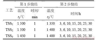
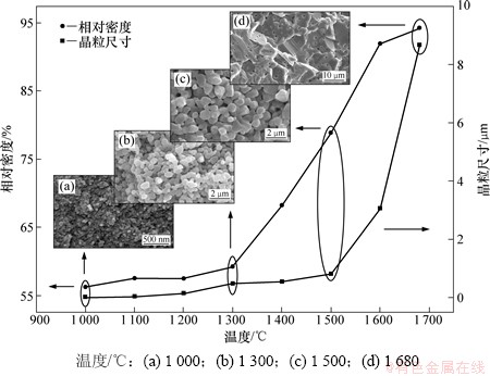
ͼ1��ʾΪ�ڲ�ͬ�¶ȵ��ս������BeO ��������ܶȵı仯�������ͼ1�ɼ��������ս�ʱ����ӳ�������ܶ������ӣ��������ս���ڽ����ܻ��ٶȽϿ졣������1 450 ���ս�0.5 h֮�������ܶ�Ϊ79.6%���Ը����жϱ�75%����ˣ�����BeO��������ս�ʱ��1�����¶�t1Ӧ�ø���1 450 �档
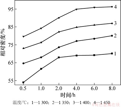
ͼ2��ʾΪ�ڲ�ͬ�¶ȵ��ս������BeO ����ƽ�������ߴ�ı仯�������ͼ2�ɼ�������ͬ�����£������ս��¶ȵ����ߣ������ߴ������ӡ����ս��¶�Ϊ1 300 ��ʱ�������ߴ�ʼ��С��1 ��m�������ս��¶�Ϊ1 450 ��ʱ�������ʼʱ�̵ľ����ߴ��Ѿ�����1 ��m��Ϊ1.77 ��m��������ѧ���ۿ�֪���ս᱾��������DE(��ʣ������)�뾧��(����)�ߴ�d֮��������¹�ϵ[17]��
ͼ1 �ڲ�ͬ�¶����ս�BeO ���������ܶ���ʱ��ı仯
Fig. 1 Relative density of specimens as a function of sintering time at various temperatures
 (1)
(1)
ʽ�У���svΪ��-�������ܣ�J/m2��WmΪĦ��������g/mol��SpΪ�ȱ��������thΪ�����ܶȡ������ߴ�Խϸ���ȱ����Խ�����ս����ܻ�������ҲԽ����ˣ�Ϊ�˱�֤��2�����ս����ܻ��������������ߴ�Ӧ�ý�ϸ�������¶�t1Ӧ�ýϵ͡�
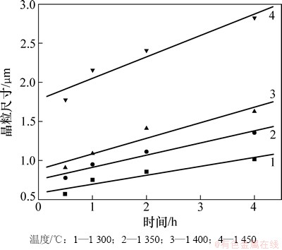
���⣬�ս��¶ȶԾ�����ò���кܴ��Ӱ�졣ͼ3��ͼ4��ʾ�ֱ�ΪBeO �����ڲ�ͬ�¶����ս�0.5��2 h���ɨ��羵��Ƭ���ɼ��������ս��¶ȵ����ߣ�������ò�ɱ�ԵԲ������������ת��Ϊ���������״�����������������������������������������ܻ����������ӡ�Ҳ����˵���ڶ����ս�ĵ����ս���ӳ��ս�ʱ�䣬�������ľ�����״Խ��������ôҲ������������մɡ���˴Ӿ�����ò����������1���ս�ҲӦ���ڽϵ��¶��½��С�
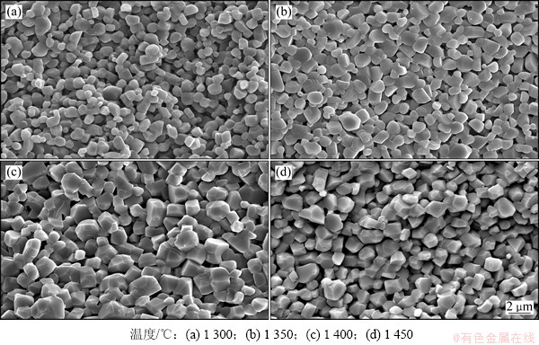
ͼ5��ʾΪ����BeO �����ڲ�ͬ�¶����ս�
1 min�������ܶȡ������ߴ������֯�ṹ���ɼ��������ս��¶ȵ����ߣ�����ľ����ߴ������ӣ�ͬʱ���ſ��������ٵ��պϿ��������ӣ��Ӷ�����ܶ�Ҳ�����ӡ����ս��¶�Ϊ1 000 ��ʱ�����徧���ߴ������ܶȷֱ�Ϊ0.045 ��m��56.3%�������ս��¶�200 �棬���徧���ߴ������ܶȷֱ�������0.5 ��m��59.3%�����ս��¶ȸ���1 300 ��֮�����徧���ߴ���������С������ߣ��������ܻ����ʼ������ߡ����ս��¶�����1 500 ��ʱ�����徧��Ϊ�������ҳߴ�Ϊ0.835 ��m��ͬʱ����ܶ�Ϊ78.9%���Ѹ���75%���˺��������ս��¶ȣ������ߴ���������Ҳ�ϴ���ȵ���ߡ����ԣ������屣�ָ��������ܻ���ͬʱ�������ߴ�Ҳ�Խϸߵ��������ӡ����ս��¶�����1 680 ��ʱ����������ܶȴﵽ94.3%�������ߴ�����8.67 ��m�����Ǿ����ڲ����ںܶ������ˣ�Ϊ�����㾭����1���ս����������ܶȸ���75%�Ҿ�����ϸ��Ҫ��t1Ӧ����1 500 �档�ɼ����Բ�������BeO�����Ʊ���������ж����ս�ʱ����1�����ս��¶�t1��ΧΪ1 450 ���t1��1 500 �档
ͼ2 �ڲ�ͬ�¶����ս�BeO ����ľ����ߴ���ʱ��ı仯
Fig. 2 Grain size of specimens as a function of sintering time at various temperatures
ͼ3 BeO �����ڲ�ͬ�¶����ս�0.5 h������֯�ṹ
Fig. 3 Microstructures of specimens sintered for 0.5 h at various temperatures
ͼ4 BeO �����ڲ�ͬ�¶����ս�2 h������֯�ṹ
Fig. 4 Microstructures of specimens sintered for 2 h at various temperatures
ͼ5 �ڲ�ͬ�¶����ս�1 min����Ʒ������ܶȡ������ߴ������֯�ṹ
Fig. 5 Relative densities, grain sizes and microstructure of specimens sintered at various temperatures for 1 min
��ͼ2����֪���������ս��¶������£������ߴ���ʱ������Թ�ϵ�������е����ݽ���������Ͽ�֪[18]��1 300��1 350��1 400��1 450 ����¶ȵľ�����������(б��)�ֱ�Ϊ0.115��0.155��0.198��0.274 ��m/h���������������ʹ������������������γɱպϵľ��ڿף��������Ի��ϸ���������մɣ���������BeO��������ս�ʱ��2�����¶�t2Ӧ�ýϵ͡�����t2����Ҳ���ܻ�������մ�[12]����ˣ��ۺϿ��Ǿ�����ò�뾧���������ʣ�ȷ��t2�ķ�ΧΪ������1 400 �档
���⣬��ͼ5����֪�����ս��¶Ƚϸ�ʱ�������屣�ָ��������ܻ���ͬʱ�������ߴ�Ҳ�Խϸߵ��������ӡ��ر��ǣ����ս��¶ȸ���1 300 ��ʱ�����徧���ߴ���������С������ߣ��������ܻ����ʼ������ߡ���ˣ�Ϊ�˴ﵽ���徧���������ʽϵ������ܻ����ʽϸߵ�Ŀ�ģ�t2Ӧ����1 300~1 500 ��֮�䡣
2.2 ����BeO����Ķ����ս�
���������о�����ƶ����µĶ����սṤ��(��ΪTSS1)���Ƚ�������15 ��/min����������1 500 ��(t1)������1 min(Ϊȷ��¯���¶��ѵ�����¶�)��Ȼ����50 ��/min�����ʽ���1 350 ��(t2)������ڸ��¶���30 h���ڵ����ս��30 h�ڣ�ÿ���һ��ʱ���¯��ȡ��һ����Ʒ����ȷ�����ս�ʱ��ֱ�Ϊ3��6��10��15��20��25��30 h��
ͼ6��ʾΪ���ն����սṤ��TSS1����ʱBeO�����ƽ������ܶȺ;����ߴ�ı仯�������ͼ6�ɼ��������ս�Ľ��У������ߴ������Ӳ������ս����(15 h֮��)����1.6 ��m֮���Էdz��������������ӡ�ͬʱ������ܶ��������ӣ���������ϵͣ�ֱ���ӳ��ս�ʱ����30 hʱ�Ÿմﵽ90%�����ԣ��ڶ����սṤ��TSS1�Ľ��й����У���Ȼ���������������ƣ�����BeO���������ܶ�ʼ�սϵ͡��������������ԭ������ǵ�2���ս��¶�t2������ɵġ���ˣ��������������������£����������սṤ�ս�t2���ߵ�1 400 ��(��ΪTSS2)��
ͼ7��ʾΪ���յ�����Ķ����սṤ��TSS2����ʱ����ܶȺ;����ߴ�ı仯�������ͼ7�ɼ����������ս�����У�����ܶȺ;����ߴ�ı仯���ƻ�����ͬ�����ս�ǰ��(ǰ10 h֮��)�����߾��ԽϿ���������ӣ������ս�ʱ�䳤��10 h֮�������ּ��仺�������ӡ��ر��ǵ��ս�ʱ��Ϊ25~30 hʱ������ܶ�94.5%�������ֲ��䣬�������ߴ���ά����2.25 ��m���ҡ�������Ϊ���ս��ʼʱ�̾����ߴ���Խϴ��ս���������Խϵ�(ʽ(1))���Ӷ�������֧�ֳ�ʱ��ĵ�2���սᣬ�������ս��������ܶȺ;����ߴ���dz����������������䡣��ˣ��ڶ����սṤ��TSS2�Ļ����ϣ����������սṤ�ս�t1��Ϊ1 450 ��(��ΪTSS3)��
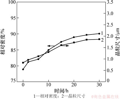
ͼ6 ���ö����սṤ��TSS1�ս����Ʒ������ܶȺ;����ߴ�
Fig. 6 Relative densities and grain sizes of specimens sintered by TSS1 process
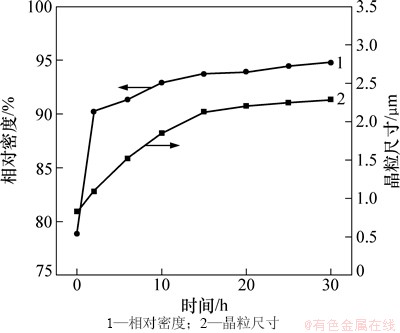
ͼ7 ���ö����սṤ��TSS2�ս������BeO ���������ܶȺ;����ߴ�
Fig. 7 Relative densities and grain sizes of nano-BeO specimens sintered by TSS2 process
ͼ8��ʾΪTSS3����������ܶȺ;����ߴ�ı仯�������ͼ8�ɼ����������ս�����У�����ܶ��ش�73.7%������96.6%�������ߴ�Ҳ�����ӣ�����������Ϊ�Ƚ�����Ȼ��Ͽ죬����ֽ�����Wang��[6, 14]���ս�������巢�����ܻ��������ߴ�仯����Ľγ�Ϊ�������ڡ�(induction time)����Ϊ��2���ս���¶Ƚϵͣ��¶ȵļ������ò��������Ծ������ἱ�糤���ڴ�ǰ���£����ս���ڣ����������ܶ���Խϵ�(��϶�ʽϸ�)�����������Ծ����ƶ����ڶ������ã���˾����Ժ��������ʳ������ս����ڣ����巢�����ܻ��������������٣��Ӷ��������ü�������˾����������ʽϿ죻���ս�ĩ�ڣ���Ȼ����ܶȽϸߣ����������ú��������ߴ�ϴ�ľ������Լ�������[12]����Ȼ������ܶȺ;����ߴ�ı仯������ս�����йء�
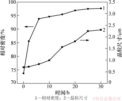
ͼ8 ���ö����սṤ��TSS3�ս����Ʒ������ܶȺ;����ߴ�
Fig. 8 Relative densities and grain sizes of specimens sintered by TSS3 process
2.3 BeO�մɵ�����֯�뵼������
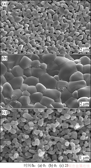
ͼ9��ʾΪ��2���ս�ʱ��Ϊ0��6��25 h��ɨ��羵��Ƭ����ͼ9��֪����TSS3�ĵ�2���ս��ʼʱ��(0 h)��������òΪ�����Σ������ս�6 h����֮���ѻ���Ӵ��������ھ��紦�����������ף�����2���ս�ʱ��Ϊ25 hʱ�������紦������������֮�⣬���弸����ȫ�ս����ܣ���ƽ�������ߴ�Ϊ2.25 ��m��
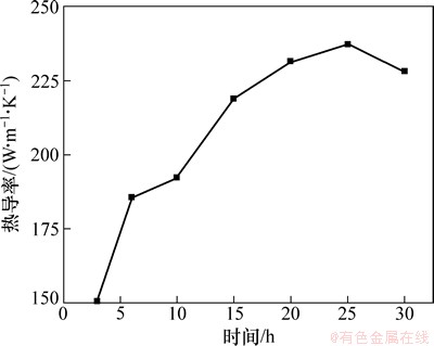
ͼ10��ʾΪ���ö����սṤ��TSS3�ս����Ʒ���ȵ��ʡ���ͼ10�ɼ����ȵ������ŵ�2���ս�ʱ����ӳ��������ӡ���ǰ������BeO�մɵĵ��Ȼ���Ϊ���Ӵ�����������Ʒ����ܶ���Ӱ���ȵ��ʵ���Ҫ���ء�������ܶ����Ŷ����սṤ��TSS3�Ľ�������(ͼ8)������ȵ��ʴ�����ͬ�ı仯���ơ���ͼ10����֪��ʵ������BeO�մɵ�����ȵ���Ϊ237 W/(m��K)����ֵԶ������ͬ����ܶ�(96.6%)��BeO�մɵ������ȵ���300 W/(m��K)����ԭ��Ϊ���Ĵ���ʹ�մɵ��ȵ����½���Enloe��[19]����AlN�մɵ��о������������ʸ���2%ʱ����ȵ��ʵ�Ӱ��ܴ���������֮�⣬BeO�մɵľ���Ҳ����Ҫ�����á�����ͨ������ʱ����ɢ��������ˣ����Ӵ������ʽ��ͣ��ȵ����½���Buhr��[20]���о�Ҳ������������Ĵ��ڻή���մɵ��ȵ��ʡ����ǹ��ھ�����ȵ��ʵ�Ӱ�컹���ڷ��硣Watari��[21-22]��Ϊ��������(�����ߴ�)���ȵ��ʵ�Ӱ�첻��
ͼ9 �������սṤ��TSS3�ս���Ʒ��ͬʱ�������֯�ṹ
Fig. 9 Microstructures of specimens sintered by TSS3 process for different times
ͼ10 �������սṤ��TSS3�ս����Ʒ���ȵ���
Fig. 10 Thermal conductivities of samples sintered by TSS3 process
2.4 ����BeO������ս����
�ս�����[6, 12, 17]�����������ս�����д���6����Ҫ���ս���ƣ�(1) ������ɢ���ơ������ɿ��������������Ǩ�ơ�(2) ����ɢ���ơ�(3) �����ۼ����ơ�����(ԭ��)�ɿ�����������ͨ�����е�����Ǩ�Ʋ������ھ��������档(4) ������ɢ���ơ�����ͨ�����������ɢǨ�ơ�(5) ����Ǩ�ƻ��ơ�����ֱ�ӽ���Ǩ�ơ�(6) �����Ǩ�ƻ��ơ��ս�����г��ֵĶ��澧��������߶������Ľ����ֱ�ӷ���Ǩ�ơ����У������Ǩ�ƻ�����һ������������ԭ����ק����Ч���ƾ��������Ļ���[23-25]��Czubayko��[24]���о��ߴ�пʱ�۲쵽���ֻ��ƣ����Ƿ��֣����¶Ƚϵ�ʱ������ק�Ŷ����С��120������Ǿ��罻����ƶ��������¶Ƚϸ�ʱ����Ǵ���120������Ǿ��罻���Ծ����ƶ�����ק���úܵ͡�
�ս�����и����ս���ƶ�����һ�������ã����Ǻ��ֻ�������Ҫ������������ս�ʱ�ں��ս��������йء����ս����(�ر��ǵ���������ܶȽϵ�ʱ)������ɢ�������������ã��������ս�ĩ�ھ�����ɢΪ��Ҫ�ս����[26]�����ս��¶Ƚϸ�ʱ���ȼ������ý�ǿ������Ǩ�ƻ��ƺͽ����Ǩ�ƻ���������[6]������ս��¶�����ʹ���ʲ�������������ѹ����ô�����ۼ�����������[27]��Mazaheri��[12]���о����������¶ȸ���1 100 ��֮������ZnO���ս����Ϊ�����ۼ����ơ�ʵ���ϣ������ս��������Ҫ���������伤���ܾ����ġ�ͼ11��ʾΪ�����ܲ�ͬ�ĸ����Ƶİ�������˹���ߣ����У�vΪ����Ǩ���ٶȣ�TΪ����ѧ�¶ȡ�
������BeO������г����ս�ʱ�����ս����(�����϶�ʽϸ߾�����������)��������ɢ��������������[17]���������սᾱ����Ǩ�ƣ��սᾱ�����ҽ�С�������ٳ����Ǹù��̶����ܻ�����û�й���[27]�������ս�Ľ��У������ɢ���ƺ;�����ɢ���Ƶ�������ͻ�������巢�����ܻ������������������γɲ��ֱպ�����(�����������ʲ�ͬ���)��ͬʱ�����������ӣ����ս�ĩ�ڣ�����Ǩ�ƻ���Ҳ�������ã��Ӷ��������ܻ���ͬʱ���������������õ�����֯����Ϊ�����ߴ�ϴ��������ߴ��쳣���ڴ��ڴ����պ�����(ͼ5(d))[4]��Wang��[4]��ǰ���о�Ҳ���������ս��¶Ƚϸ�ʱ����Ǩ�ƻ��Ƶȼ��پ�������Ļ�����������ø�Ϊͻ�������������ս��¶�Ҳ���ܽ�����⡣��ˣ����ó��湤���ս�����BeO������ѻ�������մɡ�
Ϊ���ϸ�������մɣ�������ɢ������Ǩ�ƺͽ����Ǩ�Ƶ����ھ��������Ļ��Ʊ��뱻���ƣ�ͬʱ������ɢ������ɢ���������ܻ��Ļ��ƻ�������ڡ�ͼ11���������ս��¶Ƚϵ�ʱ��������ɢ���ƺ�����ɢ��������Ҫ���á���ǰ����������������ܶȽϸ�(�ս�ĩ��)ʱ������ɢ��������ɢ�����档��ˣ���������ʼ����ܶȿɽ��ͱ�����ɢ�����á������Ƕ����ս����ڵ�1���ս��Ҫ����������ܶȸ���75%����Ҫԭ��֮һ��Wang��[6]���о�Ҳ��������ܶȸ���ijһ�ٽ�ֵ֮���ս���Ʒ���ת�䡣ͼ11�����������ս��¶ȹ��ߣ���Ǩ�ƺͽ����Ǩ�ƵȻ������ױ������ˣ������ս��еĵ�2���սṤ���ں��ʵ��¶�(t2)�½���ʱ������������Ϊ������ɢ������ɢ�Ȼ��ơ�
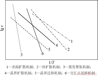
ͼ11 ���ֻ��Ƶİ�������˹����ʾ��ͼ[6, 27]
Fig. 11 Schematic representation of Arrhenius plot for sintering mechanisms[6, 27]
�����ս������֯�ṹ�仯�����볣���ս�IJ�ͬ���ڶ����ս�����У����徭��Ԥ�ȴ���(��1���ս�)������ܶ�����֮�⣬��С�������Ѿ�����(���еľ����ߴ����Ӷ����Ա�����������ʲ�һ�¶�����մ��ھ����ߴ�ֲ�������)�������Ӵ���(���ױ�Ե)�Ѿ����Բ��[28]�����⣬������ק����Ǩ�ƵĽ����Ҳ�Ѿ��γɣ��ҽϸ��¶�(t1)���γɵĽ����ļ����ܽϸߣ�������ڽϵ��¶�(t2)�¶Ծ���Ķ������ý�ǿ[23-26, 28]���ڵ�2���ս�����У���Ϊ�ս��¶�(t2)�ϵͣ���ɢ���ʽϵ�(ͼ11)��ͬʱ���硢���ױ����ͽ����ȵط���ȱ����Ҫ�ϳ���ʱ����ܹ��ﵽƽ�⣬���Ե�2���ս�ij�����Ȼ����ܶ����ӵ������ߴ�仯���������ʮ�ֻ����������ڡ������ڡ�(TSS3��ͼ8)���������ܶȼ������ӣ������ڽ�������ק����������þ���ϸС�������մɡ�ͼ12��ʾΪ�����ս�������ս������֯�ṹ�ݱ�ʾ��ͼ��
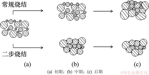
ͼ12 �����ս�������ս������֯�ṹ�ݱ�ʾ��ͼ
Fig. 12 Schematic diagram illustrating microstructure evolvement during conventional sintering and two-step sintering
3 ����
(1) ����BeO��������ս���¶ȷ�ΧΪ����1���ս��¶�t1��1 450 ���t1��1 500 �棬��2���ս��¶�t2��1 300 ���t2��1 400 �档
(2) �������������Ʊ�BeO�մɽϺ��ʵĶ����սṤ��Ϊ��(1 450 �棬1 min)+(1 400 �棬25 h)���ù����������մɵ�����֯�ṹ�Ͼ��ȣ����ܶȺ��ȵ��ʾ��ϸߣ��ֱ�Ϊ96.6%��237 W/(m��K)��
(3) ������BeO����Ķ����ս�����У�������ɢ������Ǩ�ƺͽ����Ǩ�Ƶ����ھ��������Ļ��Ʊ����ƣ�������ɢ������ɢ���������ܻ��Ļ�������Ҫ���á�
�ο����ף�
[1] ��¤��. �������մ�[M]. ����: ұ��ҵ������, 2006: 1-8.
GAO Longqiao. BeO ceramic[M]. Beijing: Metallurgical Industry Press, 2006: 1-8.
[2] Sommer M, Jan A, Henniger J. Beryllium oxide as optically stimulated luminescence dosimeter[J]. Radiation Measurements, 2008, 43(2/3/4/5/6): 353-356.
[3] �ӳ�ΰ, �ӳ�λ, ������, ��. �ߴ��ߵ���BeO �մɲ����սṤ���о�[J]. ѹ��������, 2007, 29(6): 726-728.
ZHONG Chaowei, ZHANG Shuren, LI Zhigang, et al. Studies on the sintering process of high pure BeO ceramics with high thermal conductivity[J]. Piezoel Ectectrics & Acoustooptics, 2007, 29(6): 726-728.
[4] Wang X Y, Wang R C, Peng C C, et al. Synthesis and sintering of BeO nanopowders[J]. Progress in Natural Science-Materials International, 2010, 20(1): 81-86.
[5] Chen I W, Wang X H. Sintering dense nanocrystalline ceramic without final-stage grain growth[J]. Nature, 2000, 404: 168-171.
[6] Wang X H, Chen P L, Chen I W. Two-step sintering of ceramics with constant grain-size, I: Y2O3[J]. Journal of the American Ceramic Society, 2006, 89(2): 431-437.
[7] Li J, Ye Y. Densification and grain growth of Al2O3 nanoceramics during pressureless sintering[J]. Journal of the American Ceramic Society, 2006, 89(1): 139-143.
[8]  P, Galusek D, et al. Two-stage sintering of alumina with submicrometer grain size[J]. Journal of the American Ceramic Society, 2007, 90(1): 330-332.
[9] Binner J, Annapoorani K, Paul A, et al. Dense nanocrystructured zirconia by two stages conventional/hybrid microwave sintering[J]. Journal of the European Ceramic Society, 2007, 28(5): 973-976.
[10] Mazaheri M, Valefi M, Hesabi Z R, et al. Two-step sintering of nanocrystalline 8Y2O3 stabilized ZrO2 synthesized by glycine nitrate process[J]. Ceramics International, 2009, 35(1): 13-20.
[11]  P, Capel F, Tartaj J, et al. A strategic two-stage low temperature thermal processing leading to fully dense and fine-grained doped-ZnO varistors[J]. Advance Materials, 2002, 14(2): 137-141.
[12] Mazaheri M, Zahedi A M, Sadrnezhaad S K. Two-step sintering of nanocrystalline ZnO compacts: Effect of temperature on densification and grain growth[J]. Journal of the American Ceramic Society, 2008, 91(1): 56-63.
[13] Kim H D, Han B D, Park D S, et al. Novel two-step sintering process to obtain a bimodal microstructure in silicon nitride[J]. Journal of the American Ceramic Society, 2002, 85(1): 245-252.
[14] Mohammadhossein E, Mohammadhossein F, Mahdi A. The effect of the two-step sintering process on consolidation of fluoridated hydroxyapatite and its mechanical properties and bioactivity[J]. International Journal of Applied Ceramic Technology, 2014, 11(1): 47-56.
[15] Huan Y, Wang X, Fang J, et al. Grain size effects on piezoelectric properties and domain structure of BaTiO3 ceramics prepared by two-step sintering[J]. Journal of the American Ceramic Society, 2013, 96(11): 3369-3371.
[16] Wang X, Wang R, Peng C, et al. Growth of BeO nanograins synthesized by polyacrylamide gel route[J]. Journal of Materials Science and Technology, 2011, 27(2): 147-152.
[17] ������. ��ĩ�ս�����[M]. ����: ұ��ҵ������, 2002: 15.
GUO Shiju. Powder sintering principles[M]. Beijing: Metallurgical Industry Press, 2002: 15.
[18] Wang C J, Huang C Y, Wu Y C. Two-step sintering of fine alumina-zirconia ceramics[J]. Ceramic International, 2009, 35(4): 146-1472.
[19] Enloe J H, Rice R W, Lau J W, et al. Microstructural effects on the thermal conductivity of polycrystalline aluminum nitride[J]. Journal of the American Ceramic Society, 1991, 74(9): 2214-2219.
[20] Buhr H, M��ller G. Microstructure and thermal conductivity of AlN(Y2O3) ceramics sintered in different atmospheres[J]. Journal of the European Ceramic Society, 1993, 12(4): 271-277.
[21] Watari K, Ishizaki K, Fujikawa T. Thermal conduction mechanism of aluminium nitride ceramics[J]. Journal of Materials Science, 1992, 27(10): 2627-2630.
[22] Virkar A V, Jackson T B, Cutler R A. Thermodynamic and kinetic effects of oxygen removal on the thermal conductivity of aluminum nitride[J]. Journal of the American Ceramic Society, 1989, 72(11): 2031-2042.
[23] Chen P L, Chen I W. Grain growth in CeO2: Dopant effects, defect mechanisms, and solute drag[J]. Journal of the American Ceramic Society, 1996, 79(7): 1793-1800.
[24] Czubayko L, Sursaeva V G, Gottstein G, et al. Influence of triple junctions on grain boundary motion[J]. Acta Materialia, 1998, 46(16): 5863-5871.
[25] Gottstein G, Shvindlerman L S. Triple junction dragging and von Neumann�CMullins relation[J]. Scripta Materialia, 1998, 38(10): 1541-1547.
[26] Kingery W D, Berg M. Study of initial stages of sintering solid by viscous flow, evaporation-condensation and self-diffusion[J]. Journal of Apply Physicals, 1955, 26 (10): 1205-1212.
[27] Rahaman M N. Ceramic processing and sintering[M]. New York: Marcel Dekker, 1995: 540-619.
[28] Lin F J T, Jonghe L C D, Rahaman M N. Microstructure refinement of sintered alumina by a two-step sintering technique[J]. Journal of the American Ceramic Society, 1997, 80(9): 2269-2277.
(�༭ ����ƽ)
�ո����ڣ�2013-05-25�������ڣ�2013-09-10
������Ŀ������������Ȼ��ѧ����������Ŀ(51202296)�����ϴ�ѧ��ʿ�����������Ŀ(2012��)
ͨ�����ߣ����ճ�(1965-)���У��㶫��Դ�ˣ���ʿ�����ڣ�����ˮ�������������Ϻ͵��ӷ�װ�մɵ��о����绰��0731-88836638��E-mail��wrc@csu.edu.cn
ժҪ��Ϊ�����ս���ڵľ������������ö����ս᷽���о�����BeO������սᡣ����2�������ս�ʵ��ȷ��ÿ���ս���¶ȷ�Χ֮���о�����BeO����Ķ����սṤ�գ�ͨ��ɨ�����������ͼ����������о��ս����������֯�ṹ�ı仯�����ü�����Dz��Բ��ϵ��ȵ��ʣ�����������BeO����Ķ����ս���ơ��о������������1�����ս��¶�(t1)��ΧΪ1 450 ���C.rsity, Changsha 410083, Chi8na;, Central South t1��1 500 �棻��2�����ս��¶�(t2)��ΧΪ1 300 ���t2��1 400 �棻�Ϻ��ʵĶ����սṤ��Ϊ��(1 450 �棬1 min)+(1 400 �棬25 h)���ù����������մɵ�����֯�ṹ�Ͼ��ȣ����ܶȺ��ȵ��ʾ��ϸߣ��ֱ�Ϊ96.6%��237 W/(m��K)��������BeO����Ķ����ս�����У�������ɢ������ɢ���������ܻ��Ļ�������Ҫ���á�
