

Effects of annealing temperature on microstructure and ferroelectric properties of Bi0.5(Na0.85K0.15)0.5TiO3 thin films
GONG Yue-qiu(��Ծ��)1, ZHENG Xue-jun(֣ѧ��)1, 2, GONG Lun-jun(����)1, MA Yin(�� ӱ)1,
ZHANG Da-zhi(�Ŵ�־)1, DAI Shun-hong(��˳��)1, LI Xu-jun(�����)1
1. Faculty of Materials, Optoelectronics and Physics, Xiangtan University, Xiangtan 411105, China;
2. Key Laboratory of Low Dimensional Materials and Application Technology of Ministry of Education,
Xiangtan University, Xiangtan 411105, China
Received 23 November 2009; accepted 21 January 2010
Abstracts: Bi0.5(Na0.85K0.15)0.5TiO3 (BNKT15) thin films were synthesized by metal-organic decomposition (MOD) at annealing temperatures of 650, 680, 710 and 740 ��C, and the effects of annealing temperature on the microstructure, dielectric properties, remnant polarization (2Pr) and leakage current density were studied with X-ray diffractometer, atomic force microscope, precision impedance analyzer, ferroelectric analysis station and semiconductor parameter tester. The results show that the thin film annealed at 710 ��C exhibits a typical perovskite structure without predominant orientation and a smooth surface with evenly distributed grains. 2Pr value (67.4 ��C/cm2 under 830 kV/cm) and the leakage current density (1.6��10-6 A/cm2 at 170 kV/cm) for BNKT15 thin film annealed at 710 ��C are better than those for thin films annealed at other temperatures.
Key words:
BNKT15 thin film; metal-organic decomposition; annealing temperature; remnant polarization; leakage current density;
1 Introduction
Bi0.5Na0.5TiO3 (BNT), discovered by SMOLENSKY et al in 1960, is one of the most important lead-free ferroelectric materials with perovskite crystal structure[1]. BNT ceramics show a remnant polarization (2Pr) value of 16 ��C/cm2 at 116 ��C and a high Curie temperature of 320 ��C[2], and BNT single crystal shows 2Pr value of 20 ��C/cm2 under 70 kV/cm[3]. BNT modified with Bi0.5K0.5TiO3 (BKT) shows higher 2Pr value (39.8 ��C/cm2 under 40 kV/cm) due to the corresponding rhombohedral tetragonal morphotropic phase boundary[4]. Bi0.5(Na0.85K0.15)0.5TiO3 (BNKT15) thin film annealed at 700 ��C shows 2Pr value of 27.6 ��C/cm2 under 1 000 kV/cm[5]. As mentioned above, the 2Pr values of the BNT-based materials are in the range of 16-39.8 ��C/cm2. In our previous work, we determined the best annealing temperature of 700 ��C to obtain the high remnant polarization, good fatigue endurance and retention for Bi3.25Eu0.75Ti3O12 thin film[6]. We naturally associate whether the change of annealing temperature can improve ferroelectric properties and lessen leakage current density of BNKT15 thin films. In this work, in order to find the best annealing temperature for the BNKT15 thin films with large 2Pr value, we prepared these films by metal-organic decomposition (MOD) at annealing temperatures of 650, 680, 710 and 740 ��C, respectively. The effects of annealing temperature on the microstructure, dielectric, ferroelectric properties and leakage current density of the films were investigated. The results are expected to offer useful guidelines to the ferroelectric properties design of BNT-based lead-free thin films, because the films with large 2Pr value have potential applications in nonvolatile ferroelectric random-access memories (FeRAM)[7] and micro- electromechanical systems (MEMS)[8].
2 Experimental
The BNKT15 thin films were grown on Pt/Ti/SiO2/Si(100) substrate by the metal-organic decomposition (MOD) method using a repeated coating-drying cycle. Sodium nitrate (NaNO3), potassium nitrate (KNO3), bismuth nitrate (Bi(NO3)3?5H2O) and tetrabutyl titanium (Ti(OC4H9)4) were used as starting materials for the preparation of BNKT15 precursor solution with concentration of 0.25 mol/cm3. Acetic acid (CH3COOH) and 2-methoxyethanol (CH3OCH2CH2OH) with volume ratio of 1:1 were chosen as the co-solvent. During the preparation, the tetrabutyl titanium was first dissolved in acetylacetone (CH3COCH2COCH3) in order to prevent the hydrolysis of tetrabutyl titanium caused by the moisture in air. 10% excess amount of bismuth nitrate was added to compensate for possible bismuth loss during high temperature annealing. Then, the mixture was constantly stirred for about 24 h until a transparent and stable yellow precursor solution was obtained. The precursor solution was spun on the substrate and pyrolyzed at 400 ��C for 180 s to remove residual organic ingredients. The coating-drying cycle was repeated six times to gain the desired film thickness (about 300 nm). Since the high remnant polarization and dielectric performance can be obtained by sol-gel method for BNT thin film annealed at 650 ��C[9] and BKT thin film annealed at 740 ��C[10], the annealing temperatures of 650, 680, 710 and 740 ��C were chosen. After six cycles, the prebaked thin film was annealed at the above-mentioned temperatures to promote crystallization by rapid thermal annealing process.
Phase identification and crystalline orientation of BNKT15 thin film were characterized with an X-ray diffractometer (XRD, D/Max 2550 VB, Rigaku, Japan) with Cu K�� radiation. Surface morphology, grain size and surface roughness of the thin film were identified by an atomic force microscopy (AFM, Nanoscope Multimode NS-3D, DI, USA). In order to measure ferroelectric and dielectric properties, the circular Pt top electrode with radius of 0.1 mm was deposited on the thin film using a shadow mask by DC magnetron sputtering. The polarization-electric field (P-E) hysteresis loops were measured with a ferroelectric tester (Precision Workstation, Radiant Technologies, USA) under the various applied voltages in the range from -25 to 25 V. The dielectric constant and dielectric loss were measured at the frequency range of 100 -1��106 Hz with an impedance analyzer (HP4294A, Hewlett Packard, USA). Leakage current density was measured at applied voltage of 5 V with semiconductor parameter analyzer (4200-SCS, Keithly, USA). All of the measurements were performed at room temperature.
3 Result and discussion
XRD patterns of BNKT15 thin films annealed at 650, 680, 710 and 740 ��C are given in Fig.1. The thin film annealed at 650 ��C shows mixed perovskite polycrystalline phase and pyrochlore intermediate phase. With the increase of annealing temperature, the typical intermediate phase Bi2Ti2O7 located at about 2��=30��[11] continuously transforms into the perovskite compound, and disappears at 740 ��C. All the diffraction peaks of the thin film annealed at 650 ��C are low and broad, indicating poor crystallinity. As the annealing temperature increases from 650 to 710 ��C, the diffraction peaks of the thin films become sharper and stronger, indicating improved crystallization[12]. The film annealed at 710 ��C shows a single phase of perovskite structure. When the annealing temperature increases to 740 ��C, a peak located at about 33�� is ascribed to the peak of Si (200)[13]. The volatilizations of bismuth, potassium or sodium elements at high temperature lead to the appearance of the peak of Si (200), and the similar experimental result was observed for Bi3.25La0.75Ti3O12 thin films[14]. Additionally, according to Ref.[15], the bismuth element is the main volatile elements in the BNT-base materials. We will just discuss the volatilization of bismuth in the later.

Fig.1 XRD patterns of BNKT15 thin films annealed at different annealing temperatures
AFM images of BNKT15 thin films annealed at different annealing temperatures are shown in Fig.2. The scanning area is 1 ��m �� 1 ��m, and the roots mean square (RMS) and crystallite sizes (CS) are also shown in this figure. There is fewer porosity or voids (denoted by the symbols ����) in Fig.2(b) than in Fig.2(a), which indicates that the surface quality of the thin film annealed at 680 ��C is better than that annealed at 650 ��C. At the annealing temperature of 650 ��C, the film contains fine grains but the grain boundaries cannot be distinguished easily. For films annealed at 680 ��C, the grain boundaries can be distinguished clearly[16]. In Fig.2(c), the thin film annealed at 710 ��C has a smooth surface with evenly distributed grains. The grain sizes of the BNKT15 thin films annealed at 650, 680, 710 and 740
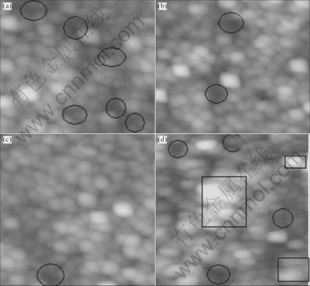
Fig.2 AFM images of BNKT15 thin films annealed at different annealing temperatures: (a) 650 ��C, RMS: 8.08 nm, CS: 94 nm; (b) 680 ��C, RMS: 8.56 nm, CS: 98 nm; (c) 710 ��C, RMS: 8.89 nm, CS: 105 nm; (d) 740 ��C, RMS: 4.79 nm, CS: 140 nm
��C are 94, 98, 105 and 140 nm, respectively. However, at the annealing temperature of 740 ��C, the crystal grains become partially agglomerated (denoted by the symbols ������) because the thin film is over-sintered, as shown in Fig.2(d). With the increase of annealing temperature, an increase of surface mobility occurs. By the growth of grains and decrease of grain boundary area, the film lowers its total energy, which leads to the increase of the grain sizes[17]. The roughness of the film surface is represented by the RMS value, which is calculated by using the equipment software routine of AFM. The RMS of the BNKT15 thin films annealed at 650, 680 and 710 ��C is 8.08, 8.56 and 8.89 nm, respectively. The roughness of the film surface increases in the annealing temperature range of 650-710 ��C, because the average crystallite size increases from 94 to 105 nm (see Figs.2(a)-2(c)). At the same time, the film becomes more granular which also results in increased surface roughness. For the thin film annealed at 740 ��C, the decrease of the RMS (4.79 nm) is the result of the partial agglomeration of grains.
The dielectric constants and dielectric losses of the BNKT15 thin films annealed at different temperatures of 650, 680, 710 and 740 ��C are described as functions of frequency in the range from 40 Hz to 1 MHz, as shown in Fig.3. The dielectric constants of the films are
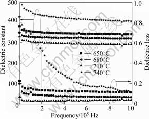
Fig.3 Dielectric constants and dielectric losses as functions of frequency for the BNKT15 thin films annealed at different temperatures
300, 325, 350 and 435, respectively, at 200 kHz, and they gradually increase with increasing annealing temperature due to larger grain size (see Fig.2) and better crystallinity (see Fig.1). As the grain size increases, the dielectric constant increases, because the large grain size will in turn result in larger polarization density[18]. Meanwhile, the dielectric loss decreases from 0.136 to 0.026 for the BNKT15 thin film annealed at 650 ��C and 710 ��C respectively, then increases to 0.500 (for the BNKT15 film annealed at 740 ��C) at 200 kHz. The decease of the dielectric loss is the result of the improvement of the microstructure, as shown in the AFM images. However, when the annealing temperature reaches 740 ��C, the exacerbated dielectric loss may be related to the diffusion and rough interface between the BNKT15 film and the bottom electrode, and thus the more charged defects are presented at the BNKT15/Pt interface[19].
In Fig.4(a), the polarization-electric field (P-E) loop of BNKT15 thin film annealed at 710 ��C is relatively saturated, while others are not saturated. The 2Pr values of BNKT15 thin films annealed at 650, 680, 710 and 740 ��C are 11.2, 16.8, 67.4 and 31.2 ��C/cm2 under 830 kV/cm of applied electric field, respectively. In order to understand the dependence of remnant polarization on annealing temperature, a function of 2Pr values with the annealing temperature is described as shown in Fig.4(b). It is obvious that the 2Pr values increase rather steeply from 680 ��C to 710 ��C because of the improved crystallization of BNKT15 thin film[7], and it is also consistent with the XRD results shown in Fig.1. Because there are intermediate phase Bi2Ti2O7 or bottom electrode (Si) in the thin films annealed at 650, 680 or 740 ��C, the P-E curves of these thin films are relatively slim. However, the 2Pr value of BNKT15 thin film annealed at 740 ��C decreases to 31.2 ��C/cm2 because Bi evaporates from the samples surface and diffuses into the bottom electrode at high annealing temperature[7]. The insufficient Bi in the prepared BNKT15 thin film results in many nonstoichiometric structural defects, leading to a degradation of the ferroelectric property[10]. Obviously, 2Pr (67.4 ��C/cm2 under 830 kV/cm) for the BNKT15 thin film annealed at 710 ��C is better than the value for the thin films annealed at other temperatures, and the enhancement of 2Pr value

Fig.4 P-E hysteresis loops of BNKT15 thin films (a), and 2Pr of BNKT15 thin films as function of annealing temperature (insert)
can increase the memory density of FeRAM[20] .
Fig.5 shows the leakage current densities of BNKT15 thin films at annealing temperatures of 650, 680, 710 and 740 ��C, and the leakage current densities are 1.2��10-3��7��10-4��1.6��10-6 and 4.4��10-3 A/cm2 at 170 kV/cm��respectively. The entire leakage current density curve has a relatively saturated planar curve before its breakdown. The film annealed at 710 ��C demonstrates the smallest leakage current density, indicating the relatively good insulating properties[21]. Because the film annealed at 710 ��C has pure and high crystallinity as shown in Fig.1, the improvement of crystallinity lessens the grain boundary effect on the resistance and leads to a small leakage current density while the intermediate phase deteriorates the leakage current densities seriously[22]. However, the leakage current density increases from 1.6��10-6 to 4.4��10-3 A/cm2 when the annealing temperature is raised from 710 to 740 ��C, and the structural defects as discussed in the P-E curve shown in Fig.4 lead to this sharp increase.
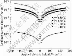
Fig.5 Leakage current density vs applied electric field of BNKT15 thin films
4 Conclusions
1) Annealing temperature has a great effect on the properties of BNKT15 thin films deposited on Pt/Ti/SiO2/Si(100) substrates. With the increase of annealing temperature, the film crystallinity increases, and it exhibits a single phase of perovskite structure at annealing temperature of 710 ��C.
2) 2Pr (67.4 ��C/cm2 under 830 kV/cm) and the leakage current density (1.6��10-6 A/cm2 at 170 kV/cm) for BNKT15 thin film annealed at 710 ��C are better than those for the thin films annealed at other temperatures.
References
[1] ISUPOV V A. Ferroelectric Na0.5Bi0.5TiO3 and K0.5Bi0.5TiO3 perovskites and their solid solutions [J]. Ferroelectrics, 2005, 315: 123-147.
[2] SMOLENSKII G A, ISUPOV V A, AGRANOVSKAYA A I, KRAINIK N N. New ferroelectrics of complex composition [J]. Soviet Phys-Solid State, 1960, 2: 2651-2654.
[3] PARK S E, CHUNG S J. Nonstoichiometry and the long-range cation ordering in crystals of (Na1/2Bi1/2)TiO3 [J]. J Am Ceram Soc, 1994, 77: 2641-2647.
[4] SASAKI A, CHIBA T, MAMIYA Y, OTSUKI E. Dielectric and piezoelectric properties of (Bi0.5Na0.5)TiO3-(Bi0.5K0.5)TiO3 systems [J]. Jpn J Appl Phys, 1999, 38: 5564-5567.
[5] YU T, KWOK K W, CHAN H L W. The synthesis of lead-free ferroelectric Bi0.5Na0.5TiO3-Bi0.5K0.5TiO3 thin films by sol-gel method [J]. Mater Lett, 2007, 61: 2117-2120.
[6] ZHENG X J, HE L, TANG M H, MA Y, WANG J B, WANG Q M. Enhancement of fatigue endurance and retention characteristic in Bi3.25Eu0.75Ti3O12 thin films [J]. Mater Lett, 2008, 62: 2876-2879.
[7] HE H Y, HUANG J F, CAO L Y. Effects of annealing schedule on orientation of Bi3.2Nd0.8Ti3O12 ferroelectric film prepared by chemical solution deposition process [J]. Mat Sci Eng B, 2006, 133: 132-135.
[8] CHENG C P, TANG M H, YE Z, ZHOU Y C, ZHENG X J, ZHONG X L, HU Z S. Ferroelectric properties of dysprosium-doped Bi4Ti3O12 thin films crystallized in various atmospheres [J]. Transaction of Nonferrous Metals Society of China, 2006, 16(s): s33-s36.
[9] CHENG C P, TANG M H, YE Z, ZHOU Y C, ZHENG X J, ZHONG X L, HU Z S. Ferroelectric properties of dysprosium-doped Bi4Ti3O12 thin films crystallized in various atomospheres [J]. Transaction of Nonferrous Metals Society of China, 2006, 16: s33-s36.
[10] YANG C H, WANG Z, XU H Y, SUN Z H, JIANG F Y, HAN J R. Preparation and main characteristics of lead-free K0.5Bi0.5TiO3 ferroelectric thin films [J]. J Cryst Growth, 2004, 262: 304-307.
[11] HOU Y D, HOU L, HUANG S Y, ZHU M K, WANG H, YAN H. Comparative study of K0.5Bi0.5TiO3 nanoparticles derived from sol-gel-hydrothermal and sol-gel routes [J]. Solid State Commun, 2006, 137: 658-661.
[12] HE L, ZHANG T, TANG M H, DENG S F. Effect of crystallization temperature on microstructure and ferroelectric property of Bi3.25Eu0.75Ti3O12 thin films prepared by MOD method [J]. Transaction of Nonferrous Metalls Society of China, 2006, 16: 1154-1158.
[13] GUO Y P, AKAI D, SAWADA K, ISHIDA M, GU M Y. Structure and electrical properties of trilayered BaTiO3/ (Na0.5Bi0.5)TiO3-BaTiO3/BaTiO3 thin films deposited on Si substrate [J]. Solid State Commun, 2009, 149: 14-17.
[14] WU Y Y, ZHANG D M, YU J, WANG Y B. Microstructure and electrical properties of Bi2O3 excess Bi3.25La0.75Ti3O12 ferroelectric ceramics [J]. Mater Chem Phys, 2009, 113: 422-427.
[15] XU Q, HUANG D P, CHEN W, LIU H X, KIM B. Effect of bismuth excess on ferroelectric and piezoelectric properties of a (Na0.5Bi0.5)TiO3�CBaTiO3 composition near the morphotropic phase boundary [J]. J Alloys Compd, 2009, 471: 310-316.
[16] KUO S Y, CHEN W C, CHENG C P. Investigation of annealing-treatment on the optical and electrical properties of sol-gel-derived zinc oxide thin films[J]. Superlattices Microstruct, 2006, 39: 162-170.
[17] CHOPRA S, SHARMA S, GOEL T C, MENDIRATT A. Effect of annealing temperature on microstructure of chemically deposited calcium modified lead titanate thin film [J]. Appl Surf Sci, 2004, 230: 207-214.
[18] ZHU X H, ZHENG D N, ZENG H, PENG W, ZHU J G, YUAN X W, YONG L P, MIAO J, LI J, TIAN H Y, XU X P. Effects of growth temperature and film thickness on the electrical properties of Ba0.7Sr0.3TiO3 thin films grown on platinized silicon substrates by pulsed laser deposition [J].Thin Solid Films, 2006, 496: 376-382.
[19] WU C H, CHU J P, WANG S F, LIN T N, CHANG W Z, JOHN V S. Effects of post annealing on the material characteristics and electrical properties of La doped BaTiO3 sputtered films [J]. Surf Coat Tech, 2008, 202: 5448-5451.
[20] SCOTT J F. Ferroelectric Memories [M]. Germany: Springer 2000: 37-45.
[21] TANG M H, ZHOU Y C, ZHENG X J, YAN Z, CHENG C P, YE Z, HU Z S. Structural and electrical properties of metal-ferroelectric-insulator-semiconductor transistors using a Pt/Bi3.25Nd0.75Ti3O12/Y2O3/Si structure [J]. Solid State Electron, 2007, 51: 371-375.
[22] HOZER L. Semiconductor ceramics: grain boundary effects [M]. New York: Ellis Harwood, 1994.
Foundation item: Projects(10672139, 10825209, 50872117) supported by the National Natural Science Foundation of China; Project(207079) supported by the Key Program of Ministry of Education of China; Project(07JJ5002) supported by the Natural Science Foundation of Hunan Province, China; Project(08C862) supported by Scientific Research Fund of Hunan Provincial Education Department, China; Project([2008]101) supported by Scientific Research Foundation for the Returned Overseas Chinese Scholars, State Education Ministry; Project([2007]362) supported by Hunan Prestigious Fu-rong Scholar Award, China
Corresponding author: ZHENG Xue-jun; Tel: +86-731-58298119; E-mail: zhengxuejun@xtu.edu.cn
DOI: 10.1016/S1003-6326(09)60393-9
