
SnAg��SnAgCu��Ǧ���Ͻ�ͷ�н����仯����
��ʱЧ�е��ݱ�
������1��������2���Ȿ��2��������1
(1. ������ҵ��ѧ ���Ͽ�ѧ�빤��ѧԺ��������100022��2. ���ݴ�ѧ �������ģ����������ݣ�350002)
ժҪ����SnAg�����Ͻ�SnAgCu�����Ͻ���Ǧ������Cu��Ni/Cu��Au/Ni/Cu�ĵ�ǥ���������Ӻ��ں��ӽ���ͺ����ڲ��γɵĽ����仯����(IMC)�����͡���ò�ͷֲ���ʽ���Լ����ӽ�ͷ�����ʱЧ������IMC�����͡��ɷֺ���ò���ݱ���ɽ����о������������������ǥ�������У�IMC�������뺸�ϳɷ��йأ���ĵ����ں��ϺϽ��е��ܽ�ȼ���ɢ�ٶ��йأ�IMC����ò������¶ȡ���ȴ�ٶȼ����ӽ�����¶��ݶ��йأ�IMC�ķֲ��뺸�ϳɷּ���ͷ�н���Ԫ�ص���ɢ�����йأ����Ͻ�ͷ�Ķ��ѻ������ͷ�Ͻ�ɷ֡�ʱЧ�¶ȡ�ʱЧʱ�䡢�غɷ�ʽ�йأ���ʱЧ�����У����Ϲ�����֯�ֻ�������ǿ���½������ѻ��ں����ڲ���������IMC��������ٽ�ߴ�ʱ��Ӧ���������أ����IMC�γɣ���Ѩ�γɼ�������IMC�������ѣ�������ǿ�Ƚӽ�������Ѳ��ַ����ں��ϣ����ַ����ڽ���IMC����
�ؼ��ʣ�
��Ǧ�����������仯������ʱЧ��
��ͼ����ţ�TN604 ���ױ�ʶ�룺A ���±�ţ�1672-7207(2007)01-0030-06
Evolution of intermetallic compounds in SnAg and SnAgCu lead-free solder joints during aging
LI Xiao-yan1, YANG Xiao-hua2, WU Ben-sheng2, YAN Yong-chang1
(1. School of Materials Science and Engineering, Beijing University of Technology, Beijing 100022, China;
2. Testing Center, Fuzhou University, Fuzhou 350002, China)
Abstract: The types, morphology and distribution of intermetallic compounds (IMCs), and the evolution of the types and composition and morphology of IMC in the joints during the following aging process were studied. The analysis results show that the types of IMCs mainly depend on solder composition and the solubility and diffusion rate of metal substrate in solder alloy; the morphology of IMC is closely related with the soldering peak temperature, cooling rate and the thermal gradient of the interface of joints; the distribution of IMC is related with solder composition and the diffusivity of metal elements in the joints. The analysis results also show that the fracture mechanism of the joints is mainly controlled by the solder composition, the peak temperature and duration of aging as well as the applied loads. The eutectic structures of the solder are coarsened during the aging process and the strength of the solder decreases, thus the fracture occurrs inside the solder. If the thickness of IMC increases to critical size, the stress concentration wil be serious. Some time multilayer IMCs will be formed and cavity will be formed and grow, the fracture will occur in the interfacial layer of IMCs. If the strengths of the solder and IMC are close during aging, the fracture will occur both inside the joints and in the interfacial layer of IMCs.
Key words: lead-free solders; intermetallic compounds; aging
�ڵ��ӷ�װ�����У������������Ӻ�֧�ŵ���Ԫ���͵�·������á��ں��Ϻͳĵ����ӽ����ϻ��ں����ڲ����������γɸ��ָ����Ľ����仯����(IMC)��IMC�Խ�ͷ�Ŀɿ���������Ҫ��������IMC��������߽�ͷǿ�ȡ���ʪ���ϼ��谭������ɢ�����������á�Ȼ������IMC������IMC�������߷ֲ���������Խ�ͷ���������Σ������ͬ�ĺ��ϺϽ�ͳĵ����γɵ�IMC�����͡��ɷ֡���ò���κ˵ص㶼��ͬ��������ʱЧ�����еı仯Ҳ��ͬ������½�ͷ���ѵĻ�����ͬ�����ǶԸ��ֳɷֵ���������ͷ�ڲ�ͬ�ĺ��ӹ��ղ������γɵ�����֯������[1-4]���Լ�������������ͷ�ڲ�ͬ��ʱЧ����������֯�����ܵ��ݱ����[5-7]���Ը������ܵ�Ӱ��[8-10]�������о����ڴˣ��������߶�Ŀǰ�о��ܶ��SnAg�����Ͻ��ϼ�SnAgCu�����Ͻ�����Cu��Ni/Cu��Au/Ni/Cu�ĵ�1�λ����������������Ӻ��ں��ӽ���ͺ����ڲ��γɵ�IMC�����͡���ò���ֲ���ʽ���������150 ������ʱЧ��ͬʱ���IMC�ijɷֺ���ò���ݱ���ɽ����о�����IMC�Ժ��Ͻ�ͷ�Ķ��ѻ��Ƶ�Ӱ����з�����
1���������ӹ�����IMC���γɹ���
1.1��SnAg���������е�IMC
Sn3.5Ag�������ϵ��۵�Ϊ221 �棬���ĺ��ӷ�ֵ�¶�ͨ����240 �����ң���SnPb�������ϵĸߺܶࡣ�����ڸú����е��ܽ�����Ҳ����Sn3.5Pb���������е�ǿ�����γɵĽ���IMC������SnPb���������еĴִ�[8, 11]���������ĵ�ΪCuʱ��Sn3.5Ag �Ͻ���Cu �����ϻ��γɽ����仯����ҽ�Cu ��Ϊ��������Cu3Sn �࣬�����ϲ�Ϊ�ȱ�״��Cu6Sn5 �࣬Ag�������������Ľ����仯����㣬������֯Ϊ����Sn����֦������Sn����Ag3Sn������ɢ�ֲ���ɵĹ�����֯[11]��
����Cu�ĵ��϶���Ni(P)�ı�������ڽ��������ȵõ���IMC�Ǿ���Сƽ��״��Ni3Sn4�࣬��Ni���ȴ���5 ��m�����ں��ӹ�����Ni������ܺõı������ã���ͼ1��ʾ[12-13]����Ni���ϳ���Ni3Sn4���Ni3Sn�� Ni3Sn2 2��IMC[14]������Cu/Ni/Cu�ĵף�����Cu�Ĵ��ڸı��˽���IMC������֯�����ϲ��Cu��ϱ�ʱ����ͷ���ȱ�״(Ni��Cu)6Sn5����Ҫ�γ��ࣻ���ں�Cu�㣬�ȱ�״(Cu��Ni)6Sn5����Ҫ�γ���, ��Ԫ(Ni��Cu)6Sn5��������ȶ�ԪCuSn��NiSn�����仯������и�ǿ��������[15]��
����Au/Ni/Cu�ĵ�Sn3.5Ag��ͷ��Au���ڵ�1�κ���ѭ�������о���ȫ���뺸���У�Ni��Sn�ڽ����γ�Ni3Sn4�࣬�ھ�����κ���ѭ�����̺�AuSn4�ں������ܽ������ɢ����������Au���ܽ�������Ag��ǿ�����ԣ�û�й۲쵽���Ե�Ag3Sn��[16]��
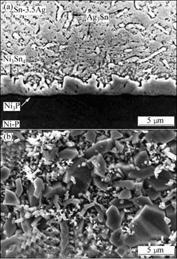
(a) ����ͼ��(b) ����ͼ
ͼ1��Sn3.5Ag������Ni(P)���ӽ�ͷ��IMC����ò���ֲ�
Fig. 1��Morphologies of IMC in Sn3.5Ag solder and Ni(P)
1.2��SnAgCu�����е�IMC
SnAgCuϵ������Ŀǰ�о��϶����Ǧ���ϣ������ɷ�ΪSn3.5Ag0.9Cu���۵�Ϊ216 �棬�������ķ�ֵ�¶�һ��Ϊ230 �档��Sn3.5Ag�Ͻ����м���С��1%��Cu������Cu�ĵĺ��ӹ����У��ȱ�״��Cu6Sn5�ܿ��ں�����ĵ������γɣ�Cu�ں��ӳ��ڶ�IMC�κ��й��ס����ԣ���Cu�ĺ��������γ�IMC������ߵ���Ԫ���Ŀɿ���������Cu�ļ�����IMC�γɺ����谭����������ϸ�����������á�����XRD���ڸոպ�����ɺ�Ľ�������������Cu3Sn�γɣ�����ɨ��羵��Ƭ��δ�۲쵽[17]����ǥ����ֵ�¶�̫�ߣ�����260 �����ң������еĽӽ������ɷֵ�SnAgCu������Cu�Ľ�ͷ�ж��γ��˾�����״Cu6Sn5�࣬�κ˵ص�Ϊ�ȱ�״Cu6Sn5�Ϸ�����Ag3Sn�����Ѩ����Ag����Խ�ߣ�����״Cu6Sn5��Խ�ࡣ������γ��������������κ˵ص��й����͵�Cu���ڣ����ҵ��ӽϸߵ�ǥ����ֵ�¶���ȴʱ�����㹻���¶��ݶȺ�ʱ��ʹ�����κ˲�������״Cu6Sn5��ǿ�ȺͶ������������Ե�Ӱ��[18]��
����Sn3.5Ag�Ͻ𣬵�����С�ڻ����1%��Cu����ʱ����������Al/Ni(V)/Cu��Ĥ�ṹ�ֱ���л�������1��5��10��20�κ��ں����ڲ�����2��IMC���ֱ�ΪCu6Sn5(��(Cu��Ni)6Sn5)��Ag3Sn��Cu6Sn5��Ҫ�����ڽ��棬Ҳ�в��ִ��Cu6Sn5�����ں����ڲ���ϸС��Ag3Sn�������ȷֲ��ں����ڲ��븻Sn�������ɢ�ֲ��Ĺ�����֯��ż�����ִ�İ�״Ag3Sn������Cu��SnAgCu�����е��ܽ��Զ������SnPb���ϵ��ܽ�ȣ�Ni���ϵ�Cu�����ϱ�����ȫ�����뺸�Ϻ��Ũ��С�����ڸú����еı����ܽ��1.54%����Cu�ں��ӹ����л�ȫ�����뺸�ϣ�����1�λ������Ӻ�IMC�ʺ��1~3 ��m�İ������ȱ�״����Cu�㱻������� Ni����Ȼ��á�����5�λ�����IMC����̬�������ȱ�״ת��Ϊ�������ȱ�״���״��������Ҳ��֮���ӡ�Ni��SnAgCu���������е���ɢ�ٶȱ���SnPb�еĿ�ܶ࣬�����Ķ�κ���ѭ�������У�����Cu6Sn5����Ƭ��ʽ���뺸�ϣ�ʹNi�㱩¶�ں����У�Ni��Cu��ͬ��Sn��Ӧ���γ�(Cu��Ni)6Sn5�����ź���ѭ�����������ӣ�Ni��(Cu��Ni)6Sn5�еĺ������ӣ�Ni�㱻(Cu��Ni)6Sn5�����ġ�����5�κ���ѭ����(Cu��Ni)6Sn5�е�Ni�ﵽ5%������20�κ���ѭ����(Cu��Ni)6Sn5�е�Ni�ﵽ6%����ͼ2��ʾ[15]�����ĵױ���û��Cu�������IMC�����ͺ���òȡ���ں��ϵĺ�Cu������Cu��(��������)С�ڵ���0.2%ʱ���ڽ����γ�������״��(Ni��Cu)3Sn4����Cu��������������0.6%ʱ�������γ��ȱ�״(Cu��Ni)6Sn5����Cu���������ڶ���֮��ʱ����������(Cu��Ni)6Sn5����������(Ni��Cu)3Sn4�������γɡ������ڸ���ͣ��5��10��20 min����������������ѭ����IMC����֯�仯�����������̵����ƣ�����֯�ݱ�Ҫ��������ʱ�Ŀ졣��һ������£��������������У��ڷ�ֵ�¶�ͣ��ʱ���ԼΪ1 min����SnAgCu��Al/Ni/Cu�Ľ�ͷ�У�����260 ��ͣ��10 minʱ��Ni���Ѿ�ȫ��������ϣ�����������ѭ��20�κ�Ni�����ʧ[15]��
����Ĥ������Auʱ����Au/Ni/Cu������Ĥ��Au�Ĵ��ڴٽ���Ni����ܽ⣬�ڵ�1�κ���ѭ�������У�50%Ni�㱻�����γ�(Cu��Ni)6Sn5���ھ���3�κ���ѭ����Ni��100%�ܽ�[19]��Au�ڵ�1��ѭ�������о����뺸�ϣ���5 min�ھͿ�����ɢ���������ӽ�ͷ���γ�AuSn4�����仯�������ò�ͷֲ��뺸��ѭ���ķ�ֵ�¶Ⱥ�ѭ�������йء�������ѭ���¶ȸߡ���ȴ�ٶ���ʱ��AuSn4����������ȡ��������γɱ���״������ѭ�����������ӣ�AuSn4�����ܽ�����������ɢ�ֲ��ں�����[16, 20]��
Ag3Sn����������ڽ�����г��֣�һ��Ϊ��״�븻Sn���γɵĺ��Ϲ�����֯����Ag�����ϸߵĺ����У����ݼ����ٶȺͺ����¶��ݶȱ仯��Ag��Sn��Ӧ�γɿ���״����֦״��Ƭ״����״�Ͱ�״��Ag3Sn��[21-22]�����ҵ�Ag����Խ��ʱ�������¶�Խ�ߣ���״��Ag3Sn��Խ��Խ�ࡣ����Ag3.8ϵ�к�Ag3.9ϵ�кϽ��ڽ��ͺ�����ȴ����ʱ����İ�״Ag3Sn��ɴ����������ӽ�ͷ�ĺ���棬��ͼ3��ʾ[18]������Ӱ���ͷ�ڳ�����Ӧ��ʱ�Ļ�е����[23]��Ȼ������Ag����С��3.2%��SnAgCu�����У���ʹ����Ҳ����������İ�״Ag3Sn��[18, 23]����Ag����Ϊ3.5%ʱ������Ԫ�Ͻ�ϵ����ӽ������ۻ���Ӧ�����õ���ɢ�Ĺ�����֯�����ҿ�����ȴ���Ա����״��Ag3Sn�����������ԣ����Ag����Ϊ3.2%~3.5%��
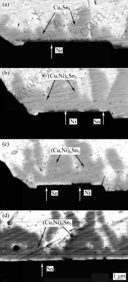
(a) 1��(b) 5��(c) 10��(d) 20��
ͼ2��������������SnAgCu������Al/Ni(V)/Cu�ĵ�ͷ��IMC�ı�ɢ��ɨ��羵��Ƭ
Fig.2��Back-scattering SEM images of IMC in Al/Ni(V)/Cu
and SnAgCu solder reflowed for different times
�������벻ͬ��Ni�㷴Ӧʱ���γɵĻ����ﲻͬ��������Ƶ�Ni-P�㣬ͨ��Ϊ������֯�������¶�Ϊ250 �棬��SnAgCu������230 ��ĺ��ӷ�ֵ�¶��£��ڽ����ϳ����γ�(Cu��Ni)6Sn5 IMC���⣬��Ni(P)��(Cu��Ni)6Sn5��֮��Ҳ�γ�Ni3P��ͺܱ�NiSnP���β㡣Ni3P�Ƚϴ࣬���к���������״�ṹ���ڸ���ͣ��ʱ��Sn��NiSnP��ͨ��Ni3P����״������Ni3P����ɢ����NiSnP�����γ�Kirkendall��Ѩ��ʹNiSnP���ɲ�����״[24]��Ni(V)���е�V�Խ�ͷ�����IMCû�����Ե�Ӱ��[15]��
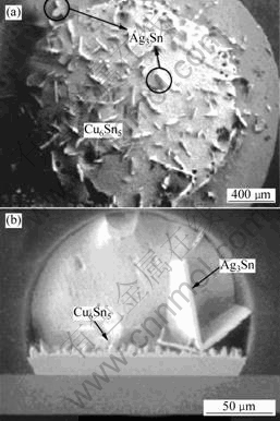
(a) Sn3.9Ag0.6Cu�Ķ���ͼ��(b) Sn3.8Ag0.7Cu�IJ���ͼ
ͼ3��Sn3.9Ag0.6Cu��Sn3.8Ag0.7Cu������
AgSn3��SEMͼ
Fig.3��SEM images of Ag3Sn in Sn3.9Ag0.6Cu
and Sn3.8Ag0.7Cu
2��ʱЧ������IMC���ݱ�
2.1��SnAg����������IMC���ݱ�
Sn3.5Ag������Cu�ĵ�ͷ���ڿ���Cu��һ���γɺ�������Cu3Sn �࣬�ڿ������ϲ��ȱ�״��Cu6Sn5 �࣬�ڻ��������еı仯�빲��SnPb���ϵı仯���ƣ���Ni��Sn3.5Ag���ϵĽ�ͷ�У����״��Ni3Sn4��ĺ���ڻػ���������ӣ��������ٶȽ�������150 ��ʱЧ 1 000 h��Ni3Sn4��û�г����ٽ���[16]������Cu/Ni/Au��Sn3.5Ag�Ľ�ͷ���ոպ��Ӻ�Au���뺸���γ���״��AuSn4�࣬����Ϊ�������״��Ni3Sn4�㣬��150 ������ʱЧʱ�����滯���ﳤ���ٶȽ��������ڸ���190 ��ʱЧʱ�������Ž���IMC�ĺ�����ӣ���IMC��������Ag3Sn��AuNiSn����������ں����ڲ�Ҳ������İ�״Ag3Sn��AuSnNi�������ͼ4��ʾ[14]���ܵ���˵��Sn3.5Ag�����еĽ���IMC��SnAgCuϵ������ȣ���ʱЧ�����еı仯����������Ǧ�����и������������ȶ��ġ�
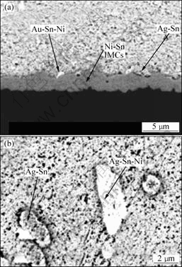
ͼ4��Sn3.5Ag��Cu/Ni/Au��ͷ��190 ��ʱЧ4 d���
IMCs(a)�������ڲ���190 ��ʱЧ8 d��IMCs��SEM��Ƭ(b)
Fig.4��SEM images of IMCs of CuNiAu and Sn3.5Ag
solder after aging for 4 d at 190 �� (a) and after aging
for 8 d at 190 �� (b)
2.2��SnAgCu������IMC���ݱ�
SnAgCu������Cu�Ľ�ͷ�ں��Ӻ��γɽ����ȱ�״��Cu6Sn5�࣬������ʱЧ�����У��ȱ�״��Cu6Sn5������������[25]������ʱЧ�¶ȵ����ߣ�Cu3Sn��Cu��Cu6Sn5��֮�������������¶�Խ�ߣ�Cu3Sn��Խ��[26]����Sn3.5Ag0.9Cu������Cu /Ni/Au�Ľ�ͷ��150 ��ʱЧ18 d��ɹ۲쵽Kirkendall�� Ѩ[22]��SnAgCu������Cu /Ni(V)/Al��Ĥ�ĺ��ӽ�ͷ��150 ����ʱЧ24 h�� Cu6Sn5��ȻΪ�ȱ�״����ʱЧ�ﵽ500 h���ȱ�״��Cu6Sn5ת��ɲ�״����Ҫָ�����ǣ���Ȼ��150 ��ʱЧʱ��IMC����̬�����ı䣬������Ȼ������ͬ���������Ni(V)����150 ��ʱЧ1 000 h����Ȼ��Cu6Sn5�������á���Cu6Sn5����û�з���Ni��������150 ��ʱNi�ڹ�̬Cu6Sn5����ɢ�dz�����[15]��
��SnAgCu������Ni���Ӻ��ݺ�����Cu������ͬ�ڽ����γ��ȱ�״(Cu��Ni)6Sn5��(Ni��Cu)3Sn4�����ǵĻ�ϲ�״�����������ʱЧ�����У�����IMC�����������ٶȽ�������ʱЧ�¶Ƚϸߡ�ʱ��ϳ�ʱ��(Cu��Ni)6Sn5������(Ni��Cu)3Sn4�����黯�ɿ������뺸���У����ǣ�IMC���ݻ����̽ϻ�������������֡�ʧ������[22]��
��SnAgCu������Au/Ni/Cu���Ӻ����γ��ȱ�״(Ni��Cu)6Sn5��ͺ����ڲ��γ���״��Cu6Sn5�࣬��ʱЧ�����У��ڽ�������γɸ��ӵ�SnNiCuAu��SnNiCuAg�����仯�������������������û�����Ϊ(Cu��Au��Ni)6Sn5�ࡣ�����Ļ�������150 ��ʱЧ8~500 h�ڼ��ȶ�����500~1 000 h֮����ٳ������ڲ���Cu6Sn5��ֻ�����ʱЧ�������ں����ڲ�����ϸ��Ƭ״��Cu6Sn5��[6]���ڸ���190 ��ʱЧʱ�����������仯�����⣬�ں����ڲ��ͽ���IMC���ϻ���������״��Ag3Sn����ʱЧ16 d��5 ��m��Ni�㱻�����ꡣ���ԣ��ڸ�����Ni��������Ҫ�Ӻ�[14]��
Ag3Sn��Ҫ���������������γɣ������仯ѧ�ȶ���ǿ����150 �����µ�ʱЧ��û�б仯��������̬��Ҫȡ���ڻ��������е�Һ̬��Ӧ��������ȴ����[22]��Ag3SnӲ���࣬С��Ag3Sn������ɢ�ֲ��ں����������ں���ǿ�ȵ���ߣ�������֦״�Ͱ�״��Ag3Sn�����ƻ��˺��ϵ������ԣ��ں��ӹ����мӿ���ȴ�ٶȿ��Կ��ƴ��Ag3Sn��������
3��IMC�Ժ��Ͻ�ͷ�Ķ��ѹ���Ӱ��
��Sn3.5Ag0.75Cu������Cu��ͷ��125 ��ʱЧ����ΪSn3.5Ag0.75Cu�������ϵ�ǿ�Ƚϸߣ�������125 ��ʱЧ�����бȽ��ȶ������ԣ�����������У�������������ں�����IMC����洦��Sn3.5Ag0.75Cu������Ni�Ľ�ͷ��ʱЧǰ����Ķ��Ѷ������ں����ڲ��������IMC����ʱЧ�����г�������� ��ʱЧǰ�����ͷǿ�ȶ����뺸����Cu�Ľ��ǿ�ȸߣ����ԣ����ϳ�Ϊ��������еı�������Sn3.5Ag0.75Cu������AuNi��ͷ�Ķ��ѻ�����ú�����Ni��ͷ�Ķ��ѻ������ƣ�������AuSn4��ɢ�ֲ��ں����У�ʹ����ǿ����ߣ����Ըý�ͷ�Ŀ���ǿ����ߣ��Ҳ���ʱЧʱ��仯����Sn3.5Ag0.75Cu������Cu�Ľ�ͷ����ǿ�����[27]��
��Ȼ���������ѻ�������ʱЧ�¶��йء�ʱЧ�¶����ߣ�������֯��IMC����ò���ɷּ��ߴ綼�ᷢ���仯�����ѻ���Ҳ�ᷢ���仯�����磬����Sn3.5Ag0.75Cu������Cu�Ľ�ͷ����ʱЧ�¶ȴ�125 �����ӵ�150 �����ߣ� Cu6Sn5������ӣ���Cu3Sn�л��γ��µ�Kirkendall��Ѩ����ԭ���Ŀ�Ѩ�������Ž���IMC������ӣ�������IMC�����Ӧ�����ӣ������������µı��β�Э�������ӣ���Ӧ������ʱ������IMC���濪�ѣ���ʱЧʱ�����ӣ�IMC��Ӧ���������������ѻ���Kirkendall��Ѩ������ [9]�����⣬�������غɺͼ����غ������£����ѻ�����ͬ������[22]�����˼��ֺ�����AuNiCu��150 ��ʱЧ�����У���ͷ�ļ��ж��ѻ���������Sn3.5Ag���ϣ����Ѷ������ں����ڲ�����ʱЧʱ���ء��۷����������������IMC����������ʱЧ1 000 h����Ȼû�дﵽ�ٽ�ߴ硣��Sn3.8Ag0.7Cu���ϣ���ʱЧʱ��Ϊ0~192 hʱ������ȫ�������ں����ڲ�������500 hʱЧ����30%�Ķ��ѷ����ڽ���IMC�������� 1 000 hʱЧ����40%�Ķ��ѷ����ڽ���IMC�����۷������������ϸС�ȱ�״��Cu6Sn5���뺸�Ͻ��ǿ�Ƚϸߣ�����ʱЧʱ���ӳ���Cu6Sn5����������������뺸�ϵĽ��ǿ�����½������ԣ����ѴӺ����ڲ���IMC���洦�ƶ�������Sn3.5Ag�����⣬����ʱЧʱ����ӳ������ѴӺ����ڲ������IMC���ƶ��������Ӧ������������֯�˻������أ����Ѿ����������
�ں����ڲ������IMC������ʱ����������״���״��Cu6Sn5���İ�״��Ag3Sn�࣬����״���״��Cu6Sn5�Ժ��ӽ�ͷ�Ļ�е����û�����Ե�Ӱ�죬������������Ĵ�İ�״Ag3Sn�����ӽ����Ĵ��Զ����������ڲ��Ĵ�İ�״Ag3Sn�ṩ������չ·������������Դ��ʹ����ǿ�Ƚ��ͣ����Լ���ǿ��û�����Ե�Ӱ�죬ֻ��ı�������Դ����չ·�������ͽ�ͷ����չ�Բ����´��Զ���[18]��
4���ᡡ��
a. ��Ǧ����SnAg�����Ͻ�SnAgCu�����Ͻ���Cu��Ni/Cu��Au/Ni/Cu�ĵ�ǥ���γɺ��ӽ�ͷ���ں�����ĵ��漰�����ڲ��γɸ��ֽ����仯�����������Ҫ�뺸�ϳɷּ��ĵϽ�ijɷ֡����ӹ��ռ�ʱЧ�¶Ⱥ�ʱ���йء�������Cu����ͨ����������״Cu3Sn���ȱ�״Cu6Sn5������; ������Ni�Ľ�����ͨ��������(Cu��Ni)6Sn5��(Ni��Cu)3Sn4�Ͳ������״��Ni3Sn4������㡣����IMC����ʱЧ�����о����ֻ����������ӡ�
b. �����ڲ���IMCһ������״������״Cu6Sn5�����״����֦״��Ƭ״����״�Ͱ�״��Ag3Sn��AuSn4�������¶�Խ�ߣ���ȴ�ٶ�Խ���������е�IMC�ߴ�Խ�����浽���ϵ��¶��ݶȽϴ�ʱ�����״ӽ���IMC�ϳ���һά����ܳ���IMC��Ag����Խ�ߣ�Խ�����γɴ��״��Ag3Sn�������е�Ag3Sn��150 ������ʱЧ�����г������ԡ�
c. ���ӽ�ͷ�Ķ��ѻᷢ���ں����ڲ���������IMC���桢����IMC���У������������ѻ��Ƹ�ռһ����������ʱЧ�����У��������������ǿ���˻����أ����Ѿ���������������࣬��ᷢ����϶��ѡ�
�ο����ף�
[1] Abtew M, Selvaduray G. Lead-free solders in microelectronics[J]. Mater Sci Eng Rep, 2000, 27(5/6): 95-141.
[2] He M, Kumar A, Yeo P T, et al. Interfacial reaction between Sn-rich solders and Ni-based metallization[J]. Thin Solid Films, 2004,462/463: 387-394.
[3] Choi W K, Lee H M. Prediction of primary intermetallic compound formation during interfacial reaction between Sn-based solder and Ni substrate[J]. Scripta Materialia, 2002, 46(11): 777-781.
[4] Zeng K, Tu K N. Six cases of reliability study of Pb-free solder joints in electronic packaging technology[J]. Materials Science and Engineering: R, 2002, 38(2): 55-105.
[5] Tu P L, Chan Y C, Lai J K L. Effect of intermetallic compounds on the thermal fatigue of surface mount solder joints[J]. IEEE Transactions on Components, Packaging, and Manufacturing Technology: Part B, 1997, 20(1): 87-93.
[6] Pang J H L, Low T H, Xiong B S, et al. Thermal cycling aging effects on Sn�CAg�CCu solder joint microstructure,IMC and strength[J]. Thin Solid Films, 2004, 462/463: 370-375.
[7] Kim K S, Yu C H, Yang J M. Aging treatment characteristics of solder bump joint for high reliability optical module[J]. Thin Solid Films, 2004, 462/463: 402-407
[8] Amagai M, Watanabe M, Omiya M, et al. Mechanical characterization of Sn�CAg�Cbased lead-free solders[J]. Microelectronics Reliability, 2002, 42(6): 951-966.
[9] Lee H T, Chen M H, Jao H M, et al. Influence of interfacial intermetallic compound on fracture behavior of solder joints[J]. Materials and Engineering A, 2003, A358(1/2): 134-141.
[10] Zeng K, Kivilahti J K. Use of multi-component phase diagrams for predicting phase evolution in solder/conductor systems[J]. J Electr Mater, 2001, 30(1), 35-44.
[11] Kerr M, Chawla N. Creep deformation behavior of Sn�C3.5Ag solder/Cu couple at small length scales[J]. Acta Materialia, 2004, 52(15): 4527-4535.
[12] HE Min, CHEN Zhong, QI Guo-jun. Solid state interfacial reaction of Sn�C37Pb and Sn�C3.5Ag solders with Ni�CP under bump metallization[J]. Acta Materialia, 2004, 52(7): 2047-2056.
[13] Choi W K, Kang S K, Sohn Y C, et al. Study of IMC morphologies and phase characteristics affected by the reactions of Ni and Cu metallurgies with Pb-Free solder joints[C]//Proc 53st Electron Comp Technol Conf. New Orleans: IEEE Inc, 2003: 1190-1196.
[14] Sharif A, Islam M N, Chan Y C. Interfacial reactions of BGA Sn�C3.5%Ag�C0.5%Cu and Sn�C3.5%Ag solders during high-temperature aging with Ni/Cu metallization[J]. Materials Science and Engineering, 2004, 113B(3): 184-189.
[15] Li M, Zhang F, Chen W T, et al. Interfacial microstructure evolution between eutectic SnAgCu solder and Al/Ni(V)/Cu thin films[J]. J Mater Res, 2002, 17(7): 1612-1621.
[16] Alam M O, Chan Y C, Tu K N. Effect of reaction time and P-content on mechanical strength of the interfaces formed between eutectic Sn�CAg solder and Au/electroless Ni(P)/Cu bond pad[J]. J Appl Phys, 2003, 94(6): 4108-4115.
[17] Li G Y, Chen B L. Formation and growth kinetics of interfacial intermetallics in Pb-free solder joint[J]. IEEE Transactions on Components and Packaging Technologies, 2003, 26(3): 651-658.
[18] Kim K S, Huh S H, Suganuma K. Effects of intermetallic compounds on properties of Sn�CAg�CCu lead-free soldered joints[J]. Journal of Alloys and Compounds, 2003, 352(1): 226-236.
[19] Choi W J, Yeh E C C, Tu K N. Mean-time-to-failure study of flip chip solder joints on Cu/Ni(V)/Al thin film under-bump metallization[J]. Appl Phys, 2003, 94(9): 5665-5671.
[20] Alam M O, Chan Y C, Tu K N. Effect of 0.5wt.% Cu addition in the Sn-3.5%Ag solder on the interfacial reaction with Au/Ni metallization[J]. Chemistry of Materials, 2003, 15(6): 4340-4342.
[21] LI De-zhi, LIU Chang-qing, Conway P P. Characteristics of intermetallics and micromechanical properties during thermal ageing of Sn�CAg�CCu flip-chip solder interconnects[J]. Materials Science and Engineering A, 2005, A391(1/2): 95-103.
[22] Salam B, Ekere N N, Rajkumar D. Study of the interface microstructure of Sn-Ag-Cu lead-free solders and the effect of solder volume on intermetallic layer formation[C]//Proc 51st Electron Comp Technol Conf. Orlando: IEEE Inc, 2001: 471-477.
[23] Kim K S, Huh S H, Suganuma K. Effects of cooling speed on microstructure and tensile properties of Sn�CAg�CCu alloys[J]. Materials Science and Engineering A, 2002, A333(1): 106-114.
[24] Jang J W, Frear D R, Lee T Y, et al. Morphology of interfacial reaction between Pb-free solders and electroless Ni(P) under-bump-metallization[J]. J Appl Phys, 2000, 88: 6359-6363.
[25] MA Xin, WANG Feng-jiang, QIAN Yi-yu, et al. Development of Cu�CSn intermetallic compound at Pb-free solder-Cu joint interface[J]. Materials Letters, 2003, 57(22): 3361-3365.
[26] Hirose A, Yanagawa H, Ide E, et al. Joint strength and interfacial microstructure between Sn�CAg�CCu and Sn�CZn�CBi solders and Cu substrate[J]. Science and Technology of Advanced Materials, 2004, 5(1/2): 267-276.
[27] Lee H T, Chen M H. Influence of intermetallic compounds on the adhesive strength of solder joints[J]. Materials Science and Engineering A, 2002, A333(1/2): 24-34.
�ո����ڣ�2006-06-08
������Ŀ��������Ȼ��ѧ����������Ŀ(50475043)�����ҽ�������ʿ�����������Ŀ(20040005012)����������Ȼ��ѧ����������Ŀ(2052006)
����飺������(1962-)���У�������Ȫ�ˣ����ڣ���ʿ�����º��Ӳ��ϵ��о�
ͨѶ���ߣ���������Ů�����ڣ���ʿ���绰��0591-87892447-801(O)��E-mail: xhyang@fzu.edu.cn
