
Trans. Nonferrous Met. Soc. China 22(2012) 3021-3026
Evaluation on residual stresses of silicon-doped CVD diamond films using X-ray diffraction and Raman spectroscopy
CHEN Su-lin, SHEN Bin, ZHANG Jian-guo, WANG Liang, SUN Fang-hong
School of Mechanical Engineering, Shanghai Jiao Tong University, Shanghai 200240, China
Received 9 July 2012; accepted 14 October 2012
Abstract:
The effect of silicon doping on the residual stress of CVD diamond films is examined using both X-ray diffraction (XRD) analysis and Raman spectroscopy measurements. The examined Si-doped diamond films are deposited on WC-Co substrates in a home-made bias-enhanced HFCVD apparatus. Ethyl silicate (Si(OC2H5)4) is dissolved in acetone to obtain various Si/C mole ratio ranging from 0.1% to 1.4% in the reaction gas. Characterizations with SEM and XRD indicate increasing silicon concentration may result in grain size decreasing and diamond [110] texture becoming dominant. The residual stress values of as-deposited Si-doped diamond films are evaluated by both sin2�� method, which measures the (220) diamond Bragg diffraction peaks using XRD, with ��-values ranging from 0�� to 45��, and Raman spectroscopy, which detects the diamond Raman peak shift from the natural diamond line at 1332 cm-1. The residual stress evolution on the silicon doping level estimated from the above two methods presents rather good agreements, exhibiting that all deposited Si-doped diamond films present compressive stress and the sample with Si/C mole ratio of 0.1% possesses the largest residual stress of ~1.75 GPa (Raman) or ~2.3 GPa (XRD). As the silicon doping level is up further, the residual stress reduces to a relative stable value around 1.3 GPa.
Key words:
silicon-doped diamond films; silicon doping; residual stress; X-ray diffraction; Raman spectroscopy;
1 Introduction
Chemical vapor deposition (CVD) diamond film has attracted intensive investigation as protecting coating material for many mechanical components, such as drawing dies [1] and cutting tools [2], due to its extremely high hardness, wear resistance, together with a very low friction coefficient. Besides, exceptional physical properties even make the CVD diamond film a good candidate for the electronic devices [3]. However, the inevitable residual stress in the CVD diamond film, including the intrinsic stress (related to dopant introduction, structures, etc.) and the thermal stress (due to the difference in the thermal expansion coefficient between diamond film and non-diamond substrate), reduces the toughness of the film and its adhesive strength to the substrate [4]. The formation of defects caused by stress relaxation will also degrade the optical and electronic properties [5]. To reduce the residual stress in the diamond film, a variety of deposition methods have been studied by many researchers, such as interface layer, annealing and doping. Among these methods, doping a certain type of dopant into the diamond film has exhibited an impressive influence on its intrinsic stress and attracted much more and more attention in recent years. For example, FERREIRA et al [6] studied the crystalline quality of heavily boron-doped diamond films and measured the residual stresses by micro-Raman spectroscopy and X-ray diffraction. LI [7] investigated the influence of sulfur doping and boron- sulfur co-doping on stress in CVD diamond films deposited on Si substrates. However, there is little research about the silicon-doped diamond films. Thus, it is meaningful to conduct a system study on the influence of silicon doping on the residual stress, as well as the crystalline structures, of diamond films,
Techniques of evaluating the residual stress of diamond film have been reported in available literatures. Among all the measurement techniques, X-ray diffraction [8,9] is one of the most popular methods because it enables a non-destructive evaluation of surface stresses of crystalline materials, while Raman spectroscopy [10] is especially useful for the analysis of stress of carbon-based materials. These two methods have been widely used to investigate the residual stress in the doped diamond films.
In this work, four types of Si-doped diamond films with Si/C mole ratio from 0.1% to 1.4% are deposited on WC-Co substrates using a home-made bias-enhanced HFCVD apparatus and their structural features and residual stresses are investigated by SEM, XRD, and Raman spectroscopy.
2 Experimental
The Si-doped films were deposited on WC-Co substrates on a home-made bias-enhanced HFCVD apparatus. Before deposition, a two-step chemical etching procedure [11] was performed to remove the binder phase from WC-Co substrate surface because cobalt can induce interfacial graphitization and thus causes deleterious effect on the adhesion of deposited diamond films. The WC-Co substrates were dipped in the Murakami��s reagent (10 g K3 [Fe(CN)]6 + 10 g KOH + 100 mL H2O) in an ultrasonic vessel for 30 min, and then etched with Caro��s acid (30 mL H2SO4 + 70 mL H2O2) for 1 min. Murakami��s reagent attacked WC grains and roughened the substrate surface; as while, Caro��s acid oxidized the binder to soluble Co2+ compounds, thus reducing the surface cobalt concentration.
On the HFCVD apparatus, six pair-twisted tantalum wires were used as hot filaments and fixed at 9-10 mm above the substrate surface in parallel and equidistance manner. During the deposition, the temperatures of hot filaments and the substrate surface were ~2200 ��C and 800-900 ��C, respectively. A negative bias was applied to the substrate for enhancing the diamond nucleation density. Si(OC2H5)4 was dissolved in acetone with a volume ratio of 1:100, 5:100, 10:100 and 15:100, approximately corresponding to Si/C mole ratio of 0.1%, 0.5%, 1% and 1.4%.
H2 flow was kept at 200 mL/min for the whole deposit. Low gas pressure of 2333.14 Pa and high bias current of 3.5 A were adopted in the nucleation period (0.5 h) in order to enhance the diamond nucleation density. Increasing gas pressure up to 5332.88 Pa in growth period I (5 h) provided a suitable condition that allowed diamond grain growing to micron scale. It is noted that the acetone flow was increased from 85 mL/min to 120 mL/min, the gas pressure was reduced to 1999.83 Pa and the bias was set reversely as -0.1 A in the growth period II (0.5 h). This condition can result in 1) reducing the stress of deposited diamond films, and 2) inhibiting the growth of diamond grains by applying a reverse bias.
Scanning electron micrograph was adopted to investigate the surface morphology of as-deposited films; X-ray diffraction and Raman spectroscopy were used to examine their crystallographic textures and chemical structures. Furthermore, the residual stresses of all films were analyzed by XRD (sin2�� method) and Raman spectra, and the results obtained by the two methods were compared with each other.
3 Results and discussion
3.1 Characterizations of as-deposited Si-doped diamond films
SEM images of the diamond films with various Si-doping levels are shown in Fig. 1. The undoped diamond film consists of mixed pyramid-shaped and rectangle-shaped grains which are related to planes (111) and (220), respectively. The average grain size is 3-5 ��m (Fig. 1(a)). When the films are doped with Si/C mole ratios of 0.1%, 0.5% and 1%, the average size of the grains decreases to ~2 ��m and the appearance of (220) plane becomes dominant in the films. Moreover, in the film doped with Si/C mole ratio of 1% (Fig. 1(d)), the majority of grains show lamellar-shaped twin characteristics, resulting from the renucleation due to the higher level of Si-doping. As the Si/C mole ratio increases up to 1.4%, the average size of the grains further reduces to ~1 ��m (Fig. 1(e)).
XRD patterns are used to further examine the crystallographic textures of all samples, as shown in Fig. 2. By investigating the two peaks at 43.9�� and 75.3�� which are assigned to the characteristic diamond diffraction patterns of (111) and (220), respectively, it can be inferred that the undoped diamond film consists mainly of mixed [111] and [110] textures. When the Si-source is introduced (Si/C mole ratio of 0.1%), the intensity of (220) peak increases greatly compared to (111) peak, implying that [110] texture is dominant in the film. With the Si-doping level increasing to Si/C mole ratios of 0.5% and 1%, the intensity of peak (220) keeps constant compared to (111) peak. As the Si/C mole ratio grows up to 1.4%, the intensity of (111) peak increases again, but not overcomes the (220) peak, implying that this film is still dominated by [110] texture. In Fig. 3, the intensity ratio of the peak (111) to peak (220), I(111)/I(220) is plotted as a function of Si/C mole ratio which embodies the evolution. The I(111)/I(220) reduces significantly from 0.95 (undoped) to 0.5 (Si/C mole ratio of 0.1%), then to the minimum value of 0.46 (Si/C mole ratio of 1%), finally increases slightly when the doping level reaches Si/C mole ratio of 1.4%.

Fig. 1 SEM images of undoped diamond film (a) and Si-doped films with Si/C mole ratio of 0.1% (b), 0.5% (c), 1% (d) and 1.4% (e)
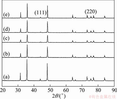
Fig. 2 XRD patterns of undoped film (a) and Si-doped films with Si/C mole ratio of 0.1% (b), 0.5% (c), 1% (d) and 1.4% (e)

Fig. 3 Intensity ratio of peak (111) to peak (220) (I(111)/I(220)) of Si-doped films deposited with various doping levels
3.2 Residual stress evaluated by XRD
X-ray diffraction is an important and non-destructive measurement technique that probes to the depth of ~600 ��m in diamond and evaluates the average stress in a larger area in sample compared with Raman spectroscopy. So, all the sample films with the thickness of 6-8 ��m can be throughout by the X-ray beam. To obtain the total residual stress ��total of the deposited film, the sin2�� method [6] was used. This technique consists of measuring the lattice spacing d of a specific (hkl) plane at different tilt angles �� (inclined exposure). The residual stress can be deduced from the relation:
 (1)
(1)
where E and �� are elastic modulus and Poisson ratio of the film, respectively; d�� is the lattice spacing at each ��; d0 is the d-value for ��=0�� (perpendicular exposure).
In this article, the (220) lattice plane was selected to determine the residual stress in the diamond films. The ��/2�� scans were measured around the (220) Bragg diffraction peak (2�ȡ�167��), from 162�� to 170��, at five tilt ��-values (0��, 20.7��, 30��, 37.8�� and 45��). For each ��-value, the central peak position is found, which belongs to the K��1 line by fitting the (220) X-ray curves with a double Gaussian. Taking the 1.4% Si/C mole ratio silicon-doped diamond film as an example, the Bragg diffraction angle 2�� was calculated and plotted as a function of sin2�� (Fig. 4).
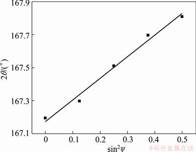
Fig. 4 Bragg diffraction angle 2�� vs sin2�� for diamond film doped with Si/C mole ratio of 1.4%
Using Eq. (1), the total residual stress ��total is obtained from the slope of the curve in Fig.4 and 143 GPa of E and 0.07 of �� are used [12]. The positive slope in Fig. 4 corresponds to a compressive residual stress in the film. The total residual stress of each sample is obtained from the sin2�� method similarly and is plotted as a function of the silicon doping level in Fig. 5.
The total residual stress is always compressive and obviously nonlinear with the increasing Si-doping level. At the low doping level (Si/C mole ratio of 0.1%), the total compressive stress increases significantly from around 1 GPa (undoped) to 2.3 GPa. Then it decreases to about 1.3, 1.5, and 1.2 GPa for the cases with Si/C mole ratios of 0.5%, 1% and 1.4%, respectively. It is noted that the stresses in the doped films all exceed that in the undoped film and the maximum value is obtained in the film with the lowest doping level.
Combining the results obtained from SEM and XRD, it can be deduced that the variation of residual stress is predominately related to the characteristic crystalline features (grain size, twins, and texture) of those Si-doped diamond films. In principle, textures [111] and [100] have the maximum and minimum elastic modulus, respectively, suggesting that texture [111] has a mass of grains with higher elastic modulus to realize small strain (small stress), while textures [110] and [100] have large strain (large stress) [16]. Therefore, the enhanced texture [110] in the film doped with Si/C mole ratio of 0.1% results in the increase of compressive stress with respect to the case of undoped film, which has more texture [111]. Moreover, some available research works indicate that the smaller grain sizes lead to larger tensile stress [6] and twins are helpful to release the accumulative stress of films [14]. In this work, however, the Si-doped diamond film with a smaller grain size presents a larger compressive residual stress, which suggests that the surface texture may play a more significant role, compared with the influence of grain size, on the residual stress of Si-doped diamond films at this doping level. With the doping level growing up to Si/C mole ratio of 0.5%, the stress declines in the presence of grains with abundant twin structures. For the doping level with Si/C mole ratio varying from 0.5% to 1.4%, the stresses in the films keep nearly constant because the grain size, twin quantity and textures in the films slightly change.

Fig. 5 Total residual stress ��total obtained from sin2�� as function of Si-doping level.
3.3 Residual stress estimated by Raman spectroscopy
The Raman spectroscopy is another non-destructive measurement technique that calculates the residual stress by detecting the diamond Raman peak shift from the natural diamond line at 1332 cm-1. Figure 6 shows the Raman spectra of the diamond films synthesized at various Si-doping levels. The undoped diamond film shows a pronounced Raman signal at ~1332 cm-1 which is typical Raman spectrum of micro-crystalline diamond film. Comparatively, another two peaks at ~1150 cm-1 and ~1490 cm-1 can be observed on the Raman spectra of diamond films with doping level of Si/C mole ratios of 0.1% and 0.5%, which is induced by the existence of trans-polyacetylene fragments that mainly present at grain boundaries [15]. Furthermore, the film doped with Si/C mole ratio of 0.5% shows a strong D band of graphitic carbon at ~1350 cm-1 and the diamond films with higher Si/C mole ratio present weaker trans- polyacetylene peaks and more pronounced diamond peak. In addition, the G band for sp2 site around 1580 cm-1 is evident in the film doped with Si/C mole ratio of 1.4%.

Fig. 6 Raman spectra of undoped diamond film (a) and diamond films deposited with Si/C mole ratio of 0.1% (b), 0.5% (c), 1% (d) and 1.4% (e)
The residual stress, ��Raman, determined from the red shifts of zone-center phonon diamond Raman peak is based on the equation ��Raman=-A����0, where ����0 is the Raman shift from the natural diamond line at 1332 cm-1 and A is the empirical constant (e.g., 0.345, 1.08 or 0.384 GPa/cm-1) [16]. We use the value 0.345 GPa/cm-1 because of its similarity in form to the CVD grown diamond films [6]. This value leads to the relation:  GPa/cm-1.
The total residual stresses of all sample films are calculated following this procedure and the results as a function of the Si-doping level are plotted in Fig. 7. The stresses are all compressive and the variation trend agrees with the results obtained by XRD method. The residual stress increases when the doping level is as low as Si/C mole ratio of 0.1%, then decreases to a value (1.3 GPa) lower than the stress in the undoped film (1.47 GPa) and keeps nearly constant when the doping degree continues to increase. Impurities and the sp2 bonding at the grain boundaries are the main sources of internal compressive stresses [13]. It is reasonable that the least doped diamond film possesses the largest residual stress because there are obvious peaks around 1150 cm-1 and 1490 cm-1 in the Raman spectra which are assigned to trans-polyacetylene fragments that mainly present at grain boundaries.

Fig. 7 Total residual stress ��total obtained from Raman spectra as function of Si-doping level
3.4 Comparison of residual stresses measured by XRD and Raman spectroscopy
The comparative results between the residual stresses obtained from X-ray measurement and micro- Raman analysis are plotted in Fig. 8. The contribution of X-ray diffraction is more sensitive to the elastic distortion of lattices in the crystalline part of the grains, while the Raman peak shift and shape are more strongly affected by impurities at the grain boundary. It is found that the evolution of the stresses determined by the two methods is roughly similar. Stresses in all the samples are compressive and the diamond film with the Si/C mole ratio of 0.1% possesses the largest residual stress.

Fig. 8 Comparison between total residual stresses obtained from X-ray diffraction (solid square) and Raman spectroscopy (solid circle)
The results of X-ray measurements are quite representative for the ray probing through the whole depth for all films. Raman spectroscopy permits analysis of impurities and defect, especially those associated with graphitic phases [6] in spite of its contribution arising from a small sample area and penetration depth. Nevertheless, it was reported that the Raman peak shift is a combination of the redshifts of Fano interaction and stress. Since the influence of the Si-doping level on the redshift due to the Fano interaction is still unknown, we can not obtain the actual value of the stress through the Raman spectroscopy. Another source of error in the stress evaluation is the variation of the diamond elastic modulus with film quality, which is normally not considered.
4 Conclusions
1) Si-doped diamond films with various Si/C mole ratios ranging from 0.1% to 1.4% are deposited on WC-Co substrates. Investigations by SEM and XRD indicate that Si-doped diamond films are mainly of texture [110] and abundant in twin.
2) For the Si-doped diamond film, the two evolutions of its residual stress on the silicon-doping level estimated from Raman spectroscopy and XRD (sin2�� method) show rather good agreement, exhibiting that all deposited Si-doped diamond films present compressive stress and the sample with Si/C mole ratio of 0.1% possesses the largest residual stress of ~1.75 GPa (Raman) or ~2.3 GPa (XRD). As the silicon-doping level is up further, the residual stress reduces to a set of relative stable values around 1.3 GPa.
3) Besides the silicon doping level, the residual stress of Si-doped diamond film is also supposed to be largely dominated by its grain size, texture and twin quantity.
References
[1] HU Dong-ping, JI Xi-lin, LI Jian-guo, FENG Jie, FEI Jun. Preparation of diamond-coated drawing die and analysis on its properties [J]. Diamond & Abrasive Engineering, 2010, 30(3): 44-48.
[2] SUN Fang-hong, CHEN Ming, ZHANG Zhi-ming, SHEN He-sheng. Studies on fabrication and test of high quality and diamond-coated thin film tools [J]. Chinese Journal of Mechanical Engineering, 2003, 39(7): 101-106.
[3] WANG Lin-jun, ZENG Qing-kai, HUANG Jian, XU Run, TANG Ke, ZHANG Ji-jun, XIA Yi-ben. Influence of the diamond grain size on the electrical properties of nano-crystalline diamond film detectors [J]. Thin Solid Films, 2011, 520(2): 717-720.
[4] XU Feng, ZUO Dun-wen, LU Wen-zhuang, ZHANG Hai-yu, WANG Min. Mircostructure and residual stress in nanocrystalline diamond film [J]. Acta Metallurgica Sinica, 2008, 44(01): 74-78.
[5] VILA M, LOPES A B, ALMEIDA F A, FERNANDES A J S, SILVA R F. Extrinsic stress induced defects in CVD diamond [J]. Diamond and Related Materials, 2008, 17(2): 190-193.
[6] FERREIRA N G, ABRAMOF E, CORAT E J, TRAVA-AIROLDI V J. Residual stresses and crystalline quality of heavily boron-doped diamond films analysed by micro-Raman spectroscopy and X-ray diffraction [J]. Carbon, 2003, 41(6): 1301-1308.
[7] LI Rong-bin. Study of the stress in doped CVD diamond films [J]. Acta Physica Sinica, 2007, 56(6): 3428-3434.
[8] HEMPEL M, HARTING M. Characterisation of CVD grown diamond and its residual stress state [J]. Diamond and Related Materials, 1999, 8(8-9): 1555-1559.
[9] RATS D, BIMBAULT L, VANDENBULCKE L, HERBIN R, BADAWI K F. Crystalline quality and residual stresses in diamond layers by Raman and X-ray diffraction analyses [J]. Journal of Applied Physics, 1995, 78(8): 4994-5001.
[10] WINDISCHMANN H, GRAY K J. Stress measurement of CVD diamond films [J]. Diamond and Related Materials, 1995, 4(5-6): 837-842.
[11] SHEN Bin, SUN Fang-hong. Deposition and friction properties of ultra-smooth composite diamond films on Co-cemented tungsten carbide substrates [J]. Diamond and Related Materials, 2009, 18(2-3): 238-243.
[12] WINDISCHMANN H, EPPS G F, CONG Y, COLLINS R W. Intrinsic stress in diamond films prepared by microwave plasma CVD [J]. Journal of Applied Physics, 1991, 69(4): 2231-2237.
[13] BERGMAN L, NEMANICH R J. Raman and photoluminescence analysis of stress state and impurity distribution in diamond thin films [J]. Journal of Applied Physics, 1995, 78(11): 6709-6719.
[14] OHSAWA Y, TAMOU Y, KIKUCHI N, HIRAGA K, OKU T. TEM observations of diamond films produced by hot filament thermal CVD [J]. Journal of Materials Science, 1991, 26(14): 3748-3752.
[15] WEI Q, YU Z M, ASHFOLD M N R, YE J, MA L. Synthesis of micro- or nano-crystalline diamond films on WC-Co substrates with various pretreatments by hot filament chemical vapor deposition [J]. Applied Surface Science, 2010, 256(13): 4357-4364.
[16] LI Hong-dong, ZHANG Tong, LI Li, LU Xian-yi, LI Bo, JIN Zeng-sun, ZOU Guang-tian. Investigation on crystalline structure, boron distribution, and residual stresses in freestanding boron-doped CVD diamond films [J]. Journal of Crystal Growth, 2010, 312(12-13): 1986-1991.
CVD������ʯ����Ӧ����X�������������������
������, �� ��, �Ž���, �� ��, �﷽��
�Ϻ���ͨ��ѧ ��е�붯������ѧԺ���Ϻ� 200240
ժ Ҫ������X��������(XRD)����������2�ַ��������˲�ͬ��̼�ȵ�CVD������ʯ��Ĥ�IJ���Ӧ��������ƫѹ��ǿ��˿��ѧ�������װ����Ӳ�ʺϽ�������Ʊ��˲�����ʯ��Ĥ���������������Բ�ͬ��������ܽ��ڱ�ͪ����ʹ�÷�Ӧ�����еĹ�̼�ȴ�0.1%�仯��1.4%���Ӷ����Ʋ�����ʯ��Ĥ�IJ���Ũ�ȡ�SEM��XRD�ı��������ʾ�����Ź����Ũ�ȵ����ӣ����ʯ��Ĥ�ľ����ߴ��С�������ʯ(110)�ľ�������ռ�š�XRD���Dz�������Ǵ�0�㵽45��仯ʱ��Ӧ�Ľ��ʯ(220)��XRD����壬������sin2�������������ʯ��Ĥ�IJ���Ӧ��������������ͨ�������ʯ������ƫ��1332 cm-1λ�õ�ƫ��������������Ӧ����2�ַ�����õIJ���Ӧ�����Ź���Ӻ�����������ʾ�����õ�һ���ԣ����еĹ���ӽ��ʯ�IJ���Ӧ����ΪѹӦ����Si/CĦ����Ϊ0.1%�ı�Ĥ������ߵIJ���Ӧ����Ϊ~1.75 GPa (������)��~2.3 GPa (XRD��)�����Ź����Ũ�ȵĽ�һ�����ߣ���Ĥ�IJ���Ӧ�����ȶ���~1.3 GPa���ҡ�
�ؼ��ʣ�������ʯ��Ĥ������ӣ�����Ӧ����X�������䣻��������
(Edited by YANG Hua)
Foundation item: Project (51005154) supported by the National Natural Science Foundation of China; Project (12CG11) supported by the Chenguang Program of Shanghai Municipal Education Commission, China; Project (201104271) supported by the China Postdoctoral Science Foundation
Corresponding author: SHEN Bin; Tel/Fax: +86-21-3420-6556; E-mail: binshen@sjtu.edu.cn
DOI: 10.1016/S1003-6326(11)61565-3
Abstract: The effect of silicon doping on the residual stress of CVD diamond films is examined using both X-ray diffraction (XRD) analysis and Raman spectroscopy measurements. The examined Si-doped diamond films are deposited on WC-Co substrates in a home-made bias-enhanced HFCVD apparatus. Ethyl silicate (Si(OC2H5)4) is dissolved in acetone to obtain various Si/C mole ratio ranging from 0.1% to 1.4% in the reaction gas. Characterizations with SEM and XRD indicate increasing silicon concentration may result in grain size decreasing and diamond [110] texture becoming dominant. The residual stress values of as-deposited Si-doped diamond films are evaluated by both sin2�� method, which measures the (220) diamond Bragg diffraction peaks using XRD, with ��-values ranging from 0�� to 45��, and Raman spectroscopy, which detects the diamond Raman peak shift from the natural diamond line at 1332 cm-1. The residual stress evolution on the silicon doping level estimated from the above two methods presents rather good agreements, exhibiting that all deposited Si-doped diamond films present compressive stress and the sample with Si/C mole ratio of 0.1% possesses the largest residual stress of ~1.75 GPa (Raman) or ~2.3 GPa (XRD). As the silicon doping level is up further, the residual stress reduces to a relative stable value around 1.3 GPa.
