

Effect of thermal annealing on defects of upgraded metallurgical grade silicon
WU Hong-jun1, 2, 3, MA Wen-hui1, 3, CHEN Xiu-hua2, JIANG Yong1, MEI Xiang-yang1, ZHANG Cong1, WU Xing-hui2
1. National Engineering Laboratory for Vacuum Metallurgy,
Kunming University of Science and Technology, Kunming 650093, China;
2. School of Physical Science and Technology, Yunnan University, Kunming 650091, China;
3. State Key Laboratory of Silicon Materials, Zhejiang University, Hangzhou 310027, China
Received 22 October 2010; accepted 29 November 2010
Abstract:
Effect of thermal annealing on the upgraded metallurgical grade(UMG)-Si was investigated under different conditions. The dislocation, grain boundaries and preferred growth orientation of Si ingot were characterized by optical microscopy, electron back scattering diffraction (EBSD) and X-ray diffractometry (XRD), respectively. The arrange order of
Key words:
upgraded metallurgical grade (UMG-Si); annealing; dislocation density; grain boundaries;
1 Introduction
It is difficult to ensure the level of solid-liquid interface when multi-crystalline silicon (mc-Si) is cast in the directional solidification crystal growth stage because of the effect of earth��s gravity. Therefore, a large number of fine grains will be formed, which results in many grain boundaries in the silicon crystal. In addition, a lot of dislocations will be led due to the factors of uneven cooling and the difference of thermal expansion coefficient between silicon ingot and quartz crucible [1]. Similarly, it will also be a lot of dislocations and grain boundaries in the silicon crystal when industrial silicon is refined directly to upgrade metallurgical grade silicon (UMG-Si) by metallurgical methods in the directional solidification crystal growth stage. It will seriously affect the conversion efficiency of UMG-Si solar cells.
The number of dislocations and grain boundaries in the UMG-Si not only can be decreased, but also the texture with preferred orientation will be also strengthened after annealing properly. Then it will greatly enhance the conversion efficiency of solar cells [2]. Thus, annealing can improve the quality of ingot after casting by directional solidification.
Currently, there are more studies about the effect of annealing on the oxygen, carbon defects in the casting mc-Si [3-11]. However, for mc-Si produced by metallurgical method with the advantages of little pollution, low cost and great potential, there are few studies about effect of annealing on its structure defects and properties [12-14]. Particularly, the researches about influence of annealing on the dislocations and grain boundaries have not been reported. In this work, the effect on the dislocation density and preferred growth orientation of UMG-Si, and the grain boundaries of its middle position were investigated under different annealing conditions, in order to find the relevant law.
2 Experimental
2.1 Verification experiment on producing same samples
As shown in Fig. 1, with the homogeneous thermal field and the same temperature gradient, two UMG-Si ingots (A and B) were prepared. The transverse and longitudinal surface topography of ingots A and B, and the dislocation densities were investigated comparatively.
As can be seen from Fig. 2 and Fig. 3, the structures and defects of sample A are in accordance with those of sample B, indicating a reproducibility of sample preparation.
2.2 Sample preparation and experimental conditions
Firstly, five UMG-Si ingots with similar structures and defects were prepared by vacuum metallurgical method. Secondly, the head and tail were removed uniformly in proportion, which were labeled as a1, a2, a3, a4 and a5, respectively. Thirdly, a1 was directly used to study before annealing, then a2, a3, a4 and a5 were annealed at 1 000 ��C for 3 h, 1 100 ��C for 3 h, 1 200 ��C for 3 h, 1 300 ��C for 3 h, respectively. The samples were heated with the heating rate of 10 ��C/min from room temperature to target temperature, and then cooled down with the same rate, with the protection of high-purity argon. Finally, each of the ingots would be taken out three wafers by cutting into bottom position, middle position and top position according to the same percentage of length.
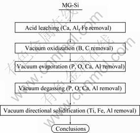
Fig. 1 Production process of UMG-Si by vacuum metallurgical method

Fig. 2 Dislocation density of ingots A and B
2.3 Experimental procedures and characterization
Figure 4 shows the experimental procedures.
Optical microscopy was used to investigate the dislocations of UMG-Si. Electron-back-scattering- diffraction (EBSD) was used to observe the grain boundaries. XRD pattern from 5�� to 100�� was used to confirm the preferred growth orientation.
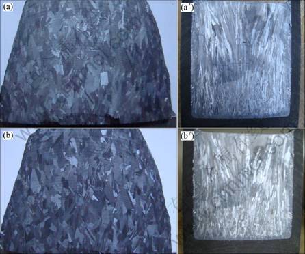
Fig. 3 Transverse section (a), (b) and longitudinal section (b), (b��) topographies of ingots A and B: (a), (a��) Ingot A; (b), (b��) Ingot B
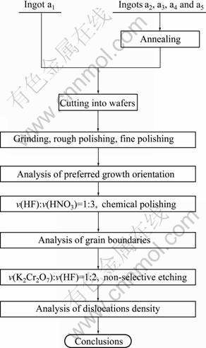
Fig. 4 Experimental procedures chart
3 Results and discussion
3.1 Effect of annealing on dislocation density
Figure 5 shows a few of UMG-Si dislocation etch pit pictures before and after annealing. It can be seen that there is not only edges dislocation, but also the screw dislocation. The shapes of dislocation etch pits are in different forms. The formations of dislocation arrays are due to a number of dislocations under the action of obstacle in the sliding process. These dislocation etch pits are in different shapes. It may be ascribed to the oxidant concentration, preferential character of etching liquid, etching time and temperature, and so on.
In addition, there are great quantities of dislocation defects in UMG-Si before annealing because of large thermal stress. However, the formation of thermal stress is due to some factors. On the one hand, it is owing to the uneven heat dissipation in the crystallization cooling process; on the other hand, the coefficients of thermal expansion are different between UMG-Si and crucible. The dislocation density in UMG-Si decreases apparently after annealing. Because the recovery process of annealing makes dislocations slip in the slip plane, cross slip or climb, making dislocations with opposite signs meet and be destroyed. What is more, it will also make a lot of dislocations from slip plane to subgrain boundary. Therefore, the dislocation density in UMG-Si is decreased eventually.
Figure 6 exhibits the average dislocation density in different positions of UMG-Si under different annealing conditions. The arrange order of dislocation density of UMG-Si ingot is from the lowest in the middle to the lower in the bottom and low in the top, which is similar to the distribution law of cast mc-Si reported in Ref. [1]
For the bottom of crystal, temperature gradient is not uniform because of the interaction of silicon liquid with the crucible. Therefore, it will result in small size grains with a lot of grain boundaries. However, atomic arrangement nearby the grain boundaries is usually extremely disordered. In addition, crystal growth rate will be adjusted to ensure the minimum defect density and high productivity in the initial growth stage, which will bring a larger temperature gradient. These two factors would make the bottom have large dislocation density. For the middle of crystal, the temperature gradient is homogeneous. Crystals continue to grow according to the adjusted rate on the condition of trying to ensure the level of solid-liquid surface and a small temperature gradient. Small grain will be swallowed gradually as crystal grows, and the grain size of the crystals will grow up gradually. Furthermore, the metal impurity concentration in the middle position is relatively low because of the effect of directional solidification segregation. So the dislocation density in the middle position is the minimum. For the top of crystal, firstly, the thermal field is constantly adjusted all times to ensure grain growth direction perpendicular to the horizontal plane. Secondly, the cooling rate is usually rapid in the later stages of crystal growth, and there will be the effect of surface tension. In addition, the metal impurities are concentrated on the top because of dephlegmation after finishing the crystal growth. All these factors lead to the largest dislocation density at the top position of UMG-Si.
Furthermore, as shown in Fig. 6, under the annealing conditions, the dislocation density in UMG-Si decreases slightly. Because the thermal stress in the UMG-Si is being released continuously in the annealing process, the dislocations are slipping and climbing, then meeting and destroying each other. Therefore, the dislocation density in UMG-Si is becoming small gradually.
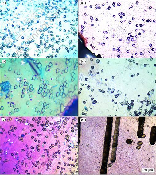
Fig. 5 Dislocation etch pit pictures of UMG-Si before(a, b, c) and after(a��, b��, c��) annealing: (a), (a��) Top position; (b), (b��) Middle position; (c), (c��) Bottom position

Fig. 6 Dislocation density of UMG-Si before and after annealing
3.2 Effect of annealing on grain boundaries
Grain boundary can be divided into two major categories such as small-angle and large-angle grain boundaries according to the difference of its structure. Ulteriorly, large angle grain boundaries can be divided into special boundaries (coincidence site lattice (CSL), express it with ��) and general grain boundaries (angle> 15��, express it with R) [15]. According to Ref. [1], the compound properties of different types of grain boundaries are different. The other grain boundaries are recombination center of minority carrier except the twin boundary ��3.
Figure 7 exhibits the information of grain boundaries at middle position of UMG-Si ingots before and after annealing, the statistics about grain boundary type and amount for each silicon wafer are average results, which are from observed eight grain boundaries in total.
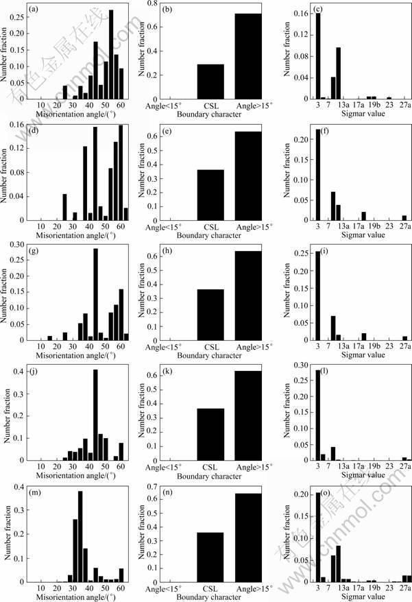
Fig. 7 Information of boundaries at middle position of UMG-Si before and after annealing: (a)-(c) Before annealing; (d)-(f) After annealing at 1 000 ��C for 3 h; (g)-(i) After annealing at 1 100 ��C for 3 h; (j)-(l) After annealing at 1 200 ��C for 3 h; (m)-(o) After annealing at 1 300 ��C for 3 h
From Fig. 7 it can be seen that, the proportion of small-angle grain boundaries, CSL and ��3 are 2%, 30% and 16%, respectively, before annealing.
From Figs. 7 (d), (g), (j), (m), under the given annealing conditions, small angle grain boundaries reduce and disappear little by little with increasing the annealing temperature. Because the UMG-Si occurred in the process of recrystallization and crystal grain growth at high temperatures, the sub-grains and small crystal grains are phagocytosed by sub-grain merger or eaten mechanism, then crystal grains grow.
As shown in Figs. 7 (e), (h), (k), (n), for large angle grain boundaries, the proportion of CSL boundary firstly increases and then decreases with increasing the annealing temperatures. This is because different recrystallization temperatures will reach different recrystallization levels. During the first stage, the R grain boundary with smaller angle is formed mainly; the CSL grain boundary with larger angle is formed mainly after a period. During the course of annealing at 1 300 ��C for 3 h, firstly, the R grain boundary is formed mainly, and the CSL grain boundary does not change apparently. Secondly, the CSL grain boundary is formed mainly; the proportion of R begins to reduce. Finally, the CSL and R vie with each other. Therefore, the temperatures above 1 300 ��C are not conducive to form the CSL grain boundary.
From Figs. 7 (f), (i), (l), (o), the ��3 grain boundary firstly increases and then decreases with increase of annealing temperature, but it is higher than that before annealing as a whole, it reaches a maximum of 28% after annealing at 1 200 ��C for 3 h. Because the driving force of grain growth comes from the total interface energy, it grows up before and after annealing. For the ��3, firstly, the atoms row on the twin plane and corresponding twin grain boundary ��3 is not wrong, which will result in the interface energy very low, so the proportion of inherent ��3 grain boundary in UMG-Si will not be changed by recrystallization. Secondly, before 1 300 ��C, it is conducive to form ��3 boundary with increase of temperature in the recrystallization process. Finally, it shows that for small crystal grains, after annealing for 3 h, too high temperature is not conducive to form ��3 boundary in the recrystallization process.
3.3 Effect of annealing on preferred growth orientation changes
The growth orientation of crystal grains has a major effect on the conversion efficiency of UMG-Si solar cells [16]. The consistency of growth orientation will accelerate the conversion efficiency of solar cells [17].
Figure 8 exhibits the preferred growth orientation of UMG-Si before and after annealing by two repeated experiments.
As can be seen from Fig. 8, the crystal grains of UMG-Si grow mainly towards the crystal planes of (111), (220), (331) and (533) before annealing. Under the given experimental conditions, the��533��and ��111�� texture peaks intensities are increasing gradually with the increase of temperature, while the others decrease to disappear before 1 200 ��C. After annealing at 1 200 ��C for 3 h, for the crystal grains in bottom, middle and top of UMG-Si ingot, they gain the best preferred growth orientation. It shows that the storage energies of (533) and (111) matrix are more than the others matrixes. In the whole annealing process, the grain boundary migration and nucleation growth rate of (533) and (111) substrates are faster than those of the other substrates. Thus, the ��533? and ��111? textures peaks intensities are increasing step by step; however, the recrystallized grains of other matrixes are merged gradually.
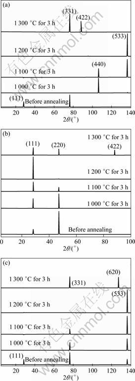
Fig. 8 Preferred growth orientation of UMG-Si before and after annealing: (a) Top; (b) Middle; (c) Bottom
During the course of annealing at 1 300 ��C for 3 h, the new textures ��422? and ��620? appear and grow competing with the main textures ��331? and ��220?. For (422) and (620) matrixes, the grain boundary characteristics of recrystallized grains are changing gradually under the annealing condition. Thus, the angles among them and neighboring grain boundaries are increasing inch by inch, and the grain boundary migration rates are increasing constantly, which will not lead to complete nucleation until the wide-angle grain boundary emerges. Then, the ��422? and ��620? textures peaks intensities are increasing step by step, and they start to grow and compete with ��331? and ��220?. Therefore, the growth of textures corresponding main peaks are inhibited.
4 Conclusions
1) The arrange order of dislocation density of UMG-Si ingot is from the lowest in the middle to the lower in the bottom and low in the top before and after annealing.
2) Under given annealing conditions, the dislocation densities in UMG-Si decrease gradually with increase of annealing temperature. The number of small angle grain boundaries decline gradually to disappear whereas the proportion of CSL grain boundaries increases firstly and then decreases.
3) After annealing at 1 200 ��C for 3 h, the dislocation densities in bottom, middle and top of UMG-Si ingot are about 4.72��105 cm-2, 4.48��105 cm-2 and 4.91��105 cm-2, respectively. Meanwhile, the twin boundary ��3 reaches the highest proportion of 28%. Furthermore, for the crystal grains in bottom position, middle position and top position of UMG-Si ingot, they all gain the best preferred growth orientations, which are ��533?, ��111? and ��533?, respectively. The best preferred growth orientation will make the strength��plasticity and ductility of UMG-Si have a better match, which will improve greatly its comprehensive mechanical properties. All these results will bring a positive effect on the following machining of silicon materials and the conversion efficiency of UMG-Si solar cells.
References
[1] YANG De-ren. Solar cell materials [M]. Beijing: Chemical Industry Press, 2007: 188. (in Chinese)
[2] ZHAO Pin, XIE Fu-zhou, SUN Zhen-guo. Material science fundamentals tutorials [M]. Harbin: Harbin Institute of Technology Press, 2001: 147. (in Chiese)
[3] DENG Hai. Investigation on the inherent impurities and defects of casting multi-crystalline silicon [D]. Hangzhou: Department of Materials Science and Engineering, Zhejiang University, 2006: 41-44. (in Chinese)
[4] YU Zheng-feng. Investigation on the oxygen defect of casting multi-crystalline silicon [D]. Hangzhou: Department of Materials Science and Engineering, Zhejiang University, 2004: 34-50. (in Chinese)
[5] REN Bin-yan, GOU Xian-fang, MA Li-fen, LI Xu-dong, XU Ying, WANG Wen-jing. Effect of thermal annealing on characteristics of multi-crystalline silicon used for solar cells [J]. Journal of Solar Energy, 2007, 28(4): 351-352. (in Chinese)
[6] REN Bin-yan, GOU Xian-fang, MA Li-fen, LI Xu-dong, XU Ying, WANG Wen-jing. Impact of thermal annealing on characteristics of polycrystalline silicon [J]. Chinese Journal of Semiconductors, 2005, 26(12): 2294-2296. (in Chinese)
[7] XI Zheng-qiang, LOU Feng, YU Zheng-feng, YANG De-ren. Investigation on the heat treatment behavior of oxygen in casting multi-crystalline silicon [J]. Journal of Transactions of Materials and Heat Treatment, 2004, 25(6): 9-10. (in Chinese)
[8] YANG De-ren, MOELLER H J. Effect of heat treatment on carbon in multicrystalline silicon [J]. Solar Energy Materials and Solar Cells, 2002, 72(1-4): 541-549.
[9] YANG De-ren, MOELLER H J. Oxygen annealing behavior in casting multi-crystalline silicon [J]. Solar Energy Materials and Solar Cells, 2000, 82: 707-712.
[10] SUN Q, YAO K H, LAGOWSKI J. Effect of carbon on oxygen precipitation in silicon [J]. Journal of Applied Physics, 1990, 67: 4313-4319. (in Chinese)
[11] YU Zheng-feng, XI Zheng-qiang, YANG De-ren, QUE Duan-lin. The formation behavior of thermal donors in cast multi-crystalline silicon [J]. Journal of Solar Energy, 2005, 26: 581. (in Chinese)
[12] XU Wen-ting. Investigation on the crystal growth and impurity defects of multi-crystalline silicon prepared by metallurgical method [D]. Kunming: College of Metallurgy and Energy, Kunming University of Science and Technology, 2008: 68-71. (in Chinese)
[13] GUO Kuan-xin. Investigation on the heat treatment and properties of multi-crystalline silicon prepared by metallurgical method [D]. Kunming: School of Physical Science and Technology, Yunnan University, 2009: 55-60. (in Chinese)
[14] ZHANG Wei-na. Electrical properties of metallurgical multi-crystalline silicon [D]. Dalian: School of Materials Science and Engineering, Dalian University of Technology, 2008: 73-74. (in Chinese)
[15] RANDLE V. The measurement of grain boundary geometry [M]. Bristol, UK: Institute of Physics Publishing, 1993: 79-89.
[16] ENDR?S A L. Mono- and tri-crystalline Si for PV application [J]. Solar Energy Materials and Solar Cells, 2002, 72: 109-124.
[17] FUJIWARA K, PAN W, SAWADA K, TOKAIRIN M, USAMI N, NOSE Y, NOMURA A, SHISHIDO T, NAKAJIMA K. Directional growth method to obtain high quality polycrystalline silicon from its melt [J]. Journal of Crystal Growth, 2006, 292: 282-285.
���˻�Գ�ұ����ȱ�ݵ�Ӱ��
����1, 2, 3, ���Ļ�1, 3, ���㻪2, �� ӽ1, ÷����1, �� ��1, ���˻�2
1. ����������ѧ ���ұ����ҹ���ʵ����, ���� 650093��
2. ���ϴ�ѧ ������ѧ�뼼��ѧԺ������ 650091��
3. �㽭��ѧ ����Ϲ����ص�ʵ���ң����� 310027
ժ Ҫ���Գ�ұ����в�ͬ�����µ����˻�ʵ���о������ý������������ӱ�ɢ�������X���������Ƿֱ���˻�ǰ��ྦྷ�費ͬ��λ��λ�����������������ȡ����б���������������˻�ǰ��ྦྷ���е�λ���ܶȴ�С�ֲ�˳��ʼ�����в����ײ��������������˻��¶ȵ����ߣ�λ���ܶ���С��С�ǶȾ��粻�ϼ��٣�ֱ����ʧ��CSL������������Ӻ��С����1 200 ��C���˻�3 h�ྦྷ���е��Ͼ������3�ﵽ28%���ྦྷ���ϡ��С��²��ľ����ֱ��������������ȡ���⽫�Ժ�������ϵļӹ����ྦྷ��̫���ܵ��ת��Ч�ʵ�����ٽ����á�
�ؼ��ʣ���ұ�裻�˻�λ���ܶȣ�����
(Edited by LI Xiang-qun)
Foundation item: Project (SKL2009-8) supported by the State Key Laboratory of Silicon Materials, Zhejiang University, China; Project (NCET-07-0387) supported by the New Century Excellent Researcher Award Program from Ministry of Education of China
Corresponding author: MA Wen-hui; Tel: +86-871-5114017; E-mail: mwhsilicon@163.com
DOI: 10.1016/S1003-6326(11)60863-7
