

Effect of poling condition on piezoelectric properties of (K0.5Na0.5)NbO3 ceramics
DU Hong-liang(�ź���)1, TANG Fu-sheng(�Ƹ���)1, LI Zhi-min(������)1,
ZHOU Wan-cheng(�����)1, QU Shao-bo(���ܲ�)2, PEI Zhi-bin(��־��)3
1. State Key Laboratory of Solidification Processing, Northwestern Polytechnical University, Xi��an 710072, China;
2. Key Laboratory of Electronic Materials Research, Ministry of Education, Xi��an Jiaotong University, Xi��an 710049, China;
3. College of Science, Air Force Engineering University, Xi��an 710051, China
Received 10 April 2006; accepted 25 April 2006
Abstract:
The lead-free piezoelectric ceramics (K0.5Na0.5)NbO3 (abbreviated as KNN) with the relative density of 97.6% were synthesized by press-less sintering owing to the careful control of processing conditions. The phase structure of KNN ceramics was analyzed. The results show that the pure perovskite phase with orthorhombic symmetry is in all ceramics specimens. The effect of poling conditions on the piezoelectric properties of KNN ceramics was investigated. The results show that the piezoelectric constant d33 and electromechanical coupling factor kp increase with poling field, poling temperature and poling time increasing, then decrease because of electric broken. Take into account of poling conditions and piezoelectric properties of pure KNN ceramics, the optimum poling conditions for pure KNN ceramics are poling field of 4 kV/mm, poling temperature of 140 �� and poling time of 20-25 min.
Key words:
(K0.5Na0.5)NbO3; lead-free piezoelectric ceramics; piezoelectric properties; poling condition; perovskite;
1 Introduction
The piezoelectric ceramics have been widely used for sensors, actuators, transducers, buzzers and other electronic devices[1, 2]. However, these piezoelectric ceramics are mostly PZT-based ceramics, which contain more than 60% lead[3]. Lead is a very toxic substances, it can cause damage to the kidney, brain and nervous system, especially the intelligence for the children[4]. Some countries have prohibited electronic devices containing lead[5]. Therefore, it is urgency to develop lead free piezoelectric ceramics to replace PZT-based ceramics. (K0.5Na0.5)NbO3 is considered to be a promising candidate of lead free piezoelectric ceramics because of its high piezoelectric properties, high Curie temperature and compatibility with human tissue[4, 6]. Recently, much attention for lead-free piezoelectric ceramics has been paid to (K0.5Na0.5)NbO3 (abbreviated as KNN)-based piezoelectric ceramics because SAITO et al had developed KNN-based textured ceramics with properties comparable to those of a basic, unmodified PZT ceramics[7]. However, pure KNN ceramics are known to be difficult to densify fully by ordinary sintering method[4, 6]. In order to improve the densification behavior and electric properties, BaTiO3[8], SrTiO3[9], LiNbO3[10], LiTaO3[11], K4CuNb8O23[12], K5.4CuTa10O29[13], CuO[14] and ZnO[15] were added into KNN ceramics. In addition, the different preparing method were used to obtain the dense KNN ceramics such as the hot pressing and spark plasma sintering[16, 17]. Despite of such difficulties in the sintering of pure KNN ceramics, the authors have succeeded in the synthesis of dense KNN ceramics sintered in air owing to the careful control of processing conditions. The poling is a very crucial step in the processing of piezoelectric ceramice, because piezoelectric ceramic has not piezoelectricity until the random ferroelectric domains are aligned through the poling [18]. Therefore, the poling process significiantly affects the piezoelectric properties. However, until now, there is no report on the effect of poling condition on piezoelectric properties of pure KNN ceramics.
In this paper, the influence of poling condition on piezoelectric properties of pure (K0.5Na0.5)NbO3 ceramics was investigated. The optimized poling condition and piezoelectric properties of KNN ceramics were achieved.
2 Experimental
The (K0.5Na0.5)NbO3 ceramics in this study were fabricated by traditional ceramics process. Reagent-grade oxide and carbonate powders of K2CO3, Na2CO3 and Nb2O5 were used as starting raw materials. Before weighing, these powders were first separately dried in an oven at 120 �� for 5 h. They were milled for 24 h using planetary milling with zirconia ball media and alcohol, and then calcined at 900 �� for 5 h. The calcined powders were ground, calcined at 900 �� for 5 h again. Then these powders were ball milled again for 12 h, dried and pressed into disks of 12 mm in diameter and 1.2 mm in thickness using PVA as a binder. After burning off PVA, the pellets were sintered at 1 100-1 120 �� for 2 h soaking period in air. The silver paste was fired on both sides of the samples at 810 �� for 20 min as the electrodes for the dielectric and piezoelectric measurements. The samples were poled in silicon oil bath under the different poling conditions.
The bulk densities of sintered samples were measured by Archimedes method. The crystal structures were determined by X-ray powder diffraction analysis using a Co K�� radiation (Philips X-Pert Diffractormeter). The microstructure evolution was observed using scanning electron microscopy (SEM, Model JSM-6360, Japan). The average grain size (diameter) was determined from the number of grains in the fixed area. The piezoelectric constant d33 was measured using a quasi-static d33 meter (Model ZJ-3, Institute of Acoustics Academic Sinica). The electromechanical coupling factor kp and mechanical quality factor Qm were calculated by the resonance-antiresonance method on the basis of IEEE standards using an impedance analyzer (Agilent 4294A).
3 Results and discussion
Fig.1 shows the XRD patterns of KNN powder calcined at 900 �� and the ceramics sintered at 1 120 ��. The phase structure in all samples is pure perovskite phase with typical orthorhombic symmetry and no any secondary impurity can be certified. Fig.2 shows the SEM micrograph of fracture surface of KNN ceramics. The microstructure of the sample sintered at 1 120 �� is uniform and fine, the grain boundary is clear, their microstructure is dense, the average grain size is about 5 ��m, the fracture surface is mainly intergranular fracture as shown in Fig.2.
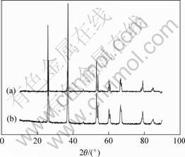
Fig.1 XRD patterns of KNN powder calcined at 900��(a) and ceramics sintered at 1 120 ��(b)

Fig.2 SEM micrograph of fracture surface of KNN ceramics sintered at 1 120 ��
Fig.3 shows d33 and kp values of KNN ceramics sintered at 1 120 �� as a function of poling field with poling time (20 min) and temperature(100 ��) being fixed as constants. It can be seen that the poling field significantly affects the piezoelectric properties of KNN ceramics, d33 and kp increase with poling field increasing in the range of 2-4 kV/mm. However, when the poling field exceeds 4 kV/mm, samples are electrically broken. The poling field can cause domain switching and rotation, make the ceramics exhibit piezoelectric properties. Because the phase structure of KNN ceramics at room is perovskite phase with orthorhombic symmetry, there are 60��, 90��, 120�� and 180�� domains in the orthorhombic phase of KNN. During the course of the poling, the 180�� domain switching has no spontaneous strain, thus the 90��, 120�� and 180�� domains can cause spontaneous strain, consequently, the 180�� domain can easily switch than 90��, 120�� and 180�� domains. It can be observed from Fig.3 that the increase of d33 and kp can result from the 180�� domain switching during lower poling field(��2 kV/mm), then 90��, 120�� and 180�� domains switching is the dominant factor affecting d33 and kp during higher poling field( 2-4 kV/mm). However, when the poling field exceeds 4 kV/mm, samples are electrically broken. This is due to pores and other physics flaws, which result in the increase of conductivity. Therefore, it is expected that the optimum poling field should be 4 kV/mm.
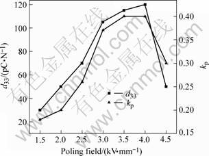
Fig.3 d33 and kp of KNN ceramics sintered at 1 120 �� as function of poling field
In order to investigate the influence of the poling temperature on the d33 and kp values of KNN ceramics sintered at 1 120 ��, all samples are polarized under the condition of poling field 4 kV/mm and poling time 20 min. Fig.4 shows the d33 and kp as a function of poling temperature with poling time and temperature. In general, the increase of poling temperature can make easily domains switching, and result in the increase of piezoelectric properties. As seen in Fig.4, the d33 and kp values increases remarkably as the poling temperature increases under 140 ��, however, when the poling temperature exceeds 140 ��, the leakage current significantly increases, KNN ceramics samples are electrically broken. Therefore, d33 and kp decrease remarkably when the poling temperature is higher than 140 ��.
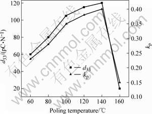
Fig.4 d33 and kp of KNN ceramics sintered at 1 120 �� as function of poling temperature
Fig.5 shows the d33 and kp values of KNN ceramics sintered at 1 120 �� as a function of poling time under the condition of poling field 4 kV/mm and poling temperature 140 ��. The variations of d33 and kp with poling time are very similar to those of the poling field and poling temperature. The d33 and kp increase remarkably with increasing the poling time in the initial period of poling. This is because that 180�� domains switching is the dominant factor affecting d33 and kp during the initial period of poling, which can easily switch than 60��, 90�� and 120�� domains. However, KNN ceramics samples are very sensitive to poling time. When the poling time exceeds 20 min, the leakage current significantly increases, KNN ceramics samples are electrically broken. This is because that the conductivity increases rapidly when the poling time exceeds 20 min.

Fig.5 d33 and kp of KNN ceramics sintered at 1 120 �� as function of poling time
Taking into account of the above results, it can be concluded that the optimum poling conditions for pure KNN ceramics are poling field of 4 kV/mm, the poling temperature of 140 �� and poling time of 20 min.
4 Conclusions
The lead-free piezoelectric ceramics (K0.5Na0.5)- NbO3 with the relative density of 97.6% have been synthesized by press-less sintering owing to the careful control of processing conditions. The optimum poling conditions for pure KNN ceramics are poling field of 4 kV/mm, poling temperature of 140 �� and poling time of 20 min.
References[1] ABRAHAM T. Applications, markets expand for piezoelectric ceramics [J]. American Ceramics Bulletin, 2000, (9): 45-47.
[2] TANI T, KIMURA T. Reactive-templated grain growth processing for lead free piezoelectric ceramics [J]. Advances in Applied Ceramics, 2006, 105(1): 55-63.
[3] CROSS E. Lead-free at last [J]. Nature, 2004, (432): 24-25.
[4] MAEDER M D, DAMJANOVIC D, SETTER N. Lead free piezoelectric materials [J]. Journal of Electroceramics, 2004, (13): 385-392.
[5] LI Y, MOON K, WONG C P. Electronics without lead [J]. Science, 308, 2005, (6): 1419.
[6] WOLNY W W. European approach to development of new environmentally sustainable electroceramics [J]. Ceramics International, 2004, 30: 1079-1083.
[7] SAITO Y, TAKAO H, TANI T, et al. Lead-free piezoceramics[J]. Nature, 2004, 432: 84-87.
[8] GUO Y, KAKIMOTO K, OHSATO H. Structure and electrical properties of lead-free (K0.5Na0.5)NbO3-BaTiO3 ceramics [J]. Japanese Journal of Applied Physics, 2004, 43: 6662-6666.
[9] GUO Y, KAKIMOTO K, OHSATO H. Dielectric and piezoelectric properties of lead-free (K0.5Na0.5)NbO3-SrTiO3 ceramics [J]. Solid State Communication, 2004, 129: 279-284.
[10] GUO Y, KAKIMOTO K, OHSATO H. Phase transitional behavior and piezoelectric properties of K0.5Na0.5)NbO3-LiNbO3 ceramics [J]. Applied Physics Letter, 2004, 85: 4121-4123.
[11] GUO Y, KAKIMOTO K, OHSATO H. (K0.5Na0.5)NbO3-LiTiO3 lead-free piezoelectric ceramics [J]. Materials Letter, 2005, 59: 241-244.
[12] MATSUBARA M, YAMAGUCHI T, KIKUTA K, et al. Sinterability and piezoelectric properties of (K,Na)NbO3 ceramics with novel sintering aid [J]. Japanese Journal of Applied Physics, 2004, 43: 7159-7163.
[13] MATSUBARA M, KIKUTA K, HIRANO S. Piezoelectric properties of (K0.5Na0.5)(Nb1-xTax)O3-K5.4CuTa10O29 ceramics [J]. Journal of Applied Physics, 2005, 97(7): 114105.
[14] MATSUBARA M, YAMAGUCHI T, SAKAMOTO W, et al. Processing and piezoelectric properties of lead-free (K, Na)(Nb, Ta)O3 ceramics [J]. Journal of American Ceramics Society, 2005, 88(5):1190-1196.
[15] PARK S H, AHN C W, NAHM S, et al. Microstructure and piezoelectric properties of ZnO-added (K0.5Na0.5)NbO3 ceramics [J]. Japanese Journal of Applied Physics, 2004, 43: 1072-1074.
[16] JAEGER R E, EGERTON L. Hot pressing of potasium-sodium niobate [J]. Journal of American Ceramics Society, 1962, 45(5): 209-213.
[17] LI J F, WANG K, ZHANG B P, et al. Ferroelectric and piezoelectric properties of fine-grained (K0.5Na0.5)NbO3 lead-free piezoelectric ceramics prepared by spark plasma sintering [J]. Journal of American Ceramics Society, 2006, 89: 706-709.
[18] JAFFE B, COOK W R, JAFFE H. Piezoelectric Ceramics [M]. New York: Academic, 1971.
Foundation item: Project(10474077) supported by the National Natural Science Foundation of China; Project(2002CB613304) supported by the National Basic Research Program of China
Corresponding author: DU Hong-liang; Tel: +86-29-88488007; E-mail: duhongliang@126.com
