

Selective growth of carbon nanotube on silicon substrates
ZOU Xiao-ping(��Сƽ) 1,2,3,4, H. ABE3, T. SHIMIZU 3, A. ANDO5, H. TOKUMOTO 3,6, ZHU Shen-ming(������)4, ZHOU Hao-shen(�ܺ���)4
1. Research Center for Sensor Technology, Beijing Information Technology Institute, Beijing 100101, China;
2. Beijing Key Laboratory for Sensor, Beijing 100101, China;
3. Nanotechnology Research Institute, National Institute of Advanced Industrial Science and Technology, 1-1-1 Higashi, Tsukuba, Ibalaki 305-8562, Japan;
4. Energy Electronics Research Institute, National Institute of Advanced Industrial Science and Technology, 1-1-1 Umezono, Tsukuba, Ibalaki 305-8568, Japan;
5. Nano-electronics Research Institute, National Institute of Advanced Industrial Science and Technology, 1-1-1 Umezono, Tsukuba, Ibalaki 305-8568, Japan;
6. Nanotechnology Research Center, Research Institute for Electronic Science,
Hokkaido University, Sapporo 001-0021, Japan
Received 10 April 2006; accepted 25 April 2006
Abstract:
The carbon nanotube (CNT) growth of iron oxide-deposited trench-patterns and the locally-ordered CNT arrays on silicon substrate were achieved by simple thermal chemical vapor deposition(STCVD) of ethanol vapor. The CNTs were uniformly synthesized with good selectivity on trench-patterned silicon substrates. This fabrication process is compatible with currently used semiconductor-processing technologies, and the carbon-nanotube fabrication process can be widely applied for the development of electronic devices using carbon-nanotube field emitters as cold cathodes and can revolutionize the area of field-emitting electronic devices. The site-selective growth of CNT from an iron oxide nanoparticle catalyst patterned were also achieved by drying-mediated self-assembly technique. The present method offers a simple and cost-effective method to grow carbon nanotubes with self-assembled patterns.
Key words:
carbon nanotubes; silicon substrate; STCVD; trench-patterned; locally-ordered pattern;
1 Introduction
Since the discovery of carbon nanotubes (CNTs) by IIJIMA[1], CNTs have attracted much interest because of many potential applications due to their unique physical and chemical properties. It is well known that carbon nanotubes have the ability to emit a cold electron at relative low voltages due to high aspect ratios and nanometer-size tips[2]. The field-emission display is one of the most advanced applications that utilize a conducting substrate to inject electrons into carbon nanotubes[3, 4]. The good field-emission properties of carbon nanotubes make them ideal candidate for the fabrication of efficient and inexpensive field-emission electronic devices. Therefore, carbon nanotubes have great potential for applications to field emitters for flat-panel field-emission displays[5] and vacuum micro-electronic devices. In practice, it is very crucial to pattern carbon nanotubes so as to correspond to each pixel[6].
For the catalyst patterning, several approaches have been mainly reported so far, such as based on standard lithographic technique[7, 8], micro-contact printing(?CP) technique[9], and ink-jet printing(IJP) technique[10]. For field-emission displays, a simple and desired device structure is a field-emission triode containing carbon nanotubes field-emitters in trench. For application of the field emission display(FED), a triode type FED has some advantages such as stable emission property, effective emission, and high-quality screen, in comparison with a diode type FED. In order to realize a CNT-based triode type FED having gate electrode structure, selective growth of CNTs onto trench- patterned substrates was considered as a key technology. How can regular arrays of carbon nanotubes be created for field-electron-emitter? A need exists to develop carbon nanotube growth techniques that are compatible with currently used semiconductor-processing technologies, in order to achieve the above goal. Recently, we have grown aligned CNT array on silicon substrate[11]. Here, the selective growth of CNTs on the trench-patterned silicon substrate and the locally-ordered carbon nanotube arrays from patterned catalyst were demonstrated by self-assembly technique on silicon substrate. A carbon nanotubes fabrication process was described, which will be of great help to develope integrated ratio-frequency amplifiers or field-emission controllable cold-electron guns for field-emission displays(FEDs).
2 Experimental
In order to grow CNTs selectively inside trench, iron-oxide deposited trench-patterns were prepared on silicon substrates. Trench-patterned silicon substrate with square rectangle and ��SE�� letter shape were employed.
To mount catalyst only on the bottom of the trenches, catalyst precursor solution was coated on the bottom of the trenches. The catalyst precursor remainsed only on the bottom of the trenches. Catalyst precursor was deposited by dropping method followed by oxidation process. Catalyst iron oxide nanoparticles were only remained at the bottom of a trench. Nanosized iron oxide particles served as a catalyst for CNT synthesis.
Using these procedures, 20 ?m deep trenches were formed with iron oxide only on the bottom of the trenches. Carbon nanotubes grew only on the places where catalysts were located.
To grow CNTs on the bottom of the trench patterns, the trench-patterned silicon substrate was mounted into a quartz tube of simple thermal CVD system, and the quartz tube was then heated up to the growth temperature in the range of 700 ��. The patterned substrate were placed on a quartz boat and then slid into the center of a quartz tube with 5 cm in diameter and 50 cm in length located in the middle of a high temperature tube furnace. Ethanol vapor, as carbon source, was introduced into the quartz tube, and carbon nanotubes were grown on the ion oxide coated patterned trench substrate via the pyrolysis of ethanol at 700 ��. For the growth of CNTs, the ethanol vapor flow through the reactor tube for 30 min at the same temperature. The length of the carbon nanotubes can be adjusted by varying the growth period. After the reaction, the quartz tube was cooled to room temperature naturally.
For locally-ordered pattern of catalyst, the catalyst precursor iron nitrate was mixed with ethanol. No surfactant was used. The catalyst precursor was patlerned on a Si substrate by using drying-mediated self-assembly method. The patterns of catalyst were subjected to thermal CVD reaction which was described above.
Scanning electron microscope (SEM; Hitachi, S-4300) was used to investigate the CNT growth on the silicon substrates. The SEM images were obtained, in order to examine the structures of the trenches formed, the growth of carbon nanotubes in the trenches and the locally-ordered carbon nanotube arrays on silicon substrate. It can be clearly seen that the selective growth of carbon nanotubes on patterned trenches and patterned catalysts has been achieved.
3 Results and discussion
It is well known that the synthesis of CNTs on trench-patterns is very difficult due to turbulence of the reaction gas flow in trench inside. To realize the selective growth of CNTs on the trench-patterns, it is necessary to optimize reaction conditions cautiously. Fig.1 shows that CNTs are selectively synthesized on the trench-patterns at 700 ��.
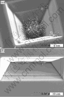
Fig.1 SEM images of CNTs grown on trench-patterned silicon substrates: (a) Square shape; (b) Rectangle shape.
The CNTs have diameters in the range of 20-30 nm. Fig.1 represents the top-view SEM images, showing that the CNTs are attached on the bottom of trench-patterned silicon substrates.
The trench-pattern has a depth of 20 ?m and a area of 20 ?m��20 ?m and 20 ?m��50 ?m on the silicon substrate. The CNTs were selectively grown on the trench-patterned silicon substrate with the optimized condition. It is well known that the growth rate of CNTs can be controlled by growth parameter. The CNTs grown on the trench-patterns can promise to fabricate the triode type FED.
Fig.2 shows the letters ��S�� and ��E�� consisting of microtrenches on silicon substrates. Carbon nanotubes grow in the trenches by employed iron oxide as catalyst located at the bottom of trenches. These carbon nanotubes can be employed as electron source of field emitter for FED.
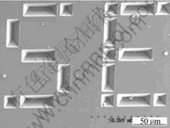
Fig.2 SEM image of CNTs grown on trench-patterned silicon substrates
The locally-ordered carbon nanotube arrays were also examined on silicon substrate. The SEM images of the CNT pattern is shown in Fig.3. It indicates that the MWCNT grows site-selectively only from the patterned catalyst. The locally-ordered hexagonal patterns have been gottern. It is important to note that the most MWCNT dots show a uniform diameter of 5 ?m and the uniform distance of about 25 ?m.
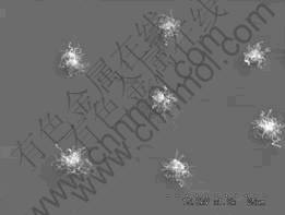
Fig. 3 Locally-ordered CNT patterns grown on top surface of SiO2/Si substrates
The locally ordered catalyst pattern formed and then carbon nanotubes were selectively grown on the catalyst patterns. The catalyst precursor solution containing iron nitrate has been cast into particle-like catalyst on the top of surface of Si substrate for forming locally ordered catalyst patterns due to the unique self-assembly capability of the solution-based catalyst precursor under the surface tension. This self-assembly process for the formation of local regular micro-patterns of catalyst particles on the top surface of Si substrate was determined by many factors[12,13], including the chemical composition and the physical properties such as surface free energy and viscosity of the solution, the surface condition such as hydrophobic or hydrophilic of the surface of silicon wafer, the stability and thickness of the dip-coated solution film on the surface of silicon wafer, and the difference in surface free energy among the solution film and silicon wafer. The schematic diagram of growth of CNT pattern is shown in Fig.4.
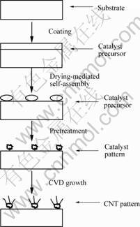
Fig. 4 Schematic diagram of growth of CNT pattern
The present drying-mediated self-assembly technique-based nanotube patterning method may find possible application in field-emission displays or other electronic devices, when it is combined with standard device fabrication processes. This method we have used is a promising method for fabricating carbon nanotube-based devices, such as field emission flat display. But the method is not limited to the patterned growth of carbon nanotubes. It also seems to pattered growth of other quasi-one-dimensional materials such as nanowires. This work provides a rational basis for generating structured assemblies of carbon nanotubes, and could eventually lead to the design of optical and electronic devices with statistically controlled meso-scope-scale features.
We believe that our method may serve as a general and simple methodology for designing and fabricating self-assembled structures with the desired multi-scale features. The effect of factors such as hydrodynamic convection, non-local interactions and film thickness on self-assembly should be investigated for better controlling formation of ordered pattern in large area.
4 Conclusions
The selective growth of the CNTs on trench-patterned silicon substrate and silicon substrate with locally-ordered catalyst pattern was demonstrated by using simple thermal CVD method. The CNTs were grown on the trench-patterns and the just growth of CNTs was suitably controlled by optimized growth conditions on the trench-patterns. The method used to obtain locally-ordered pattern catalyst by self-assembly technique is not limited to the patterned growth of carbon nanotubes. It also seems to patterned growth of other quasi-one-dimensional materials such as nanowires. These methods can be used in application of CNT-based triode structure.
Acknowledgements
This work was partially supported by Japan Science Promotion Society(JSPS) and New Energy & Industrial Technology Development Organization(NEDO) as a part of Nano Carbon Technology(NCT) Project, Japan.
References
[1] IIJIMA S. Helical microtubules of graphitic carbon [J]. Nature, 1991, 354: 56-58.
[2] RINZLER A G, HAFNER J H, NIKOLAEV P, LOU L, KIM S G, TOMANEK D, NORDLANDER P, COLBERT D T, SMALLEY R E. Unraveling nanotubes: field emission from an atomic wire [J]. Science, 1995, 269: 1550-1553.
[3] DE HEER W A, CHATELAIN A, UGARTE D. A carbon nanotube field-emission electron source [J]. Science, 1995, 270: 1179-1180.
[4] SAITO Y, HAMAGUCHI K, HATA K, UCHIDA K, TASAKA Y, IKAZAKI F, YUMURA M, KASUYA A, NISHINA Y. Conical beams from open nanotubes [J]. Nature, 1997, 389: 554-555.
[5] CHOI W B, CHUNG D S, KANG J H, KIM H Y, JIN Y W, HAN I T, LEE Y H, JUNG J E, LEE N S, PARK G S, KIM J M. Fully sealed, high-brightness carbon-nanotube field-emission display [J]. Appl Phys Lett, 1999, 75: 3129-3131.
[6] LEE Y H, JANG Y T, KIM D H, AHN J H, JU B. Realization of gated field-emitters for electrophotonic applications using carbon nanotube line emitters directly growth into submicrometer holes [J]. Adv Mater, 2001, 13: 479-482.
[7] REN Z F, HUANG Z P, WANG D Z, WEN F G, XU J W, WANG J H, CALVET L E, CHEN J, KLEMIC J F, REED M A. Growth of single freestanding multiwall carbon nanotube on each nanonickel dot [J]. Appl Phys Lett, 1999, 75: 1086-1088.
[8] HUANG S, DAI L, MAU A W H. Controlled fabrecation of large-scale alinned carbon nanofiber/nanotube patterns by photolithography [J]. Adv Mater, 2002, 14: 1140-1143.
[9] KIND H, BONARD J M, FORRO L, KERN K, HERNADI K, NILSSON L O, SCHLAPBACH L. Printing gel-like catalysts for the directed growth of multiwall carbon nanotubes [J]. Langmuir, 2000, 16: 6877-6883.
[10] AGO H, QI J, TSUKAGOSHI K, MURATA K, OHSHIMA S, AOYAGI Y, YUMURA M. Catalytic growth of carbon nanotubes and their patterning based on ink-jet and lithographic technique [J]. J Electroanal Chem, 2003, 559: 25-30.
[11] ZOU X P, ABE H, SHIMIZU T, ANDO A, NAKAYAMA Y, TOKUMOTO H, ZHU S M, ZHOU H S. Simple thermal chemical vapor deposition synthesis and electrical property of multi-walled carbon nanotubes [J]. Physica E, 2004, 24: 14-18.
[12] BOWDEN N B, WECK M, CHOI I S, WHITESIDES G M. Molecule-mimetic chemistry and mesoscale self-assembly [J]. Acc Chem Res, 2001, 34: 231-238.
[13] CARRE A, EUSTACHE F. Spreading kinetics of shear-thinning fluids in wetting and dewetting modes [J]. Langmuir, 2000, 16: 2936-2941.
. Foundation item: Project(KM200510772013) supported by the Beijing City Education Committee Science and Technology Development Program;Project( 2005-2007) supported by the Academic Innovative Team Program(Novel Sensor & Materials: Nanodevice & Nanomaterials) of Education Committee of Beijing City
Corresponding author: ZOU Xiao-ping; Tel: +86-10-64884673-812; Fax: +86-10-64879486; E-mail: xpzou2005@gmail.com
