
Trans. Nonferrous Met. Soc. China 26(2016) 1433-1438
Growth interface of CdMnTe crystal by traveling heater method
Wen-qi WU, Ji-jun ZHANG, Lin-jun WANG, Jia-hua MIN, Xu-liang WEN, Xiao-yan LIANG, Jian HUANG, Ke TANG
School of Materials Science and Engineering, Shanghai University, Shanghai 200444, China
Received 7 July 2015; accepted 28 December 2015
Abstract:
The growth interfaces of CdMnTe (CMT) crystals grown by traveling heater method (THM) were studied. Two types of polycrystalline CMT feed ingots synthesized in a traditional rocking furnace and vertical Bridgman (VB) furnace were adopted in THM growth, and the effects of the polycrystalline feed on the growth interface were revealed. The morphology of the growth interface of CMT crystal (CMT2) grown from the feed by vertical Bridgman was smoother with lower curvature compared with that of CMT crystal (CMT1) from the feed by rocking furnace. The radial Mn composition and Te inclusion distribution of the CMT wafers were analyzed and correlated to the growth interface. The Mn segregation along the radial direction and Te inclusion density of CMT2 were lower than those of CMT1. The VB method synthesized polycrystalline feed could improve the growth interface morphology, which is beneficial for decreasing the Te inclusions and Mn segregation in CMT wafers.
Key words:
CdMnTe; traveling heater method; growth interface; polycrystalline feed material ; ; ; ; ; ; ; ; ; ; ; ; ; ; ; ; ; ; ; ; ; ; ; ; ; ; ; ; ; ; ; ; ; ; ; ; ; ; ; ; ; ; ; ; ; ; ; ; ; ; ; ; ; ; ; ; ; ; ; ; ; ; ; ; ; ; ; ; ; ; ; ; ; ; ; ; ; ; ; ; ; ; ; ; ; ; ; ; ; ; ; ; ; ; ; ; ; ; ; ; ; ; ; ; ;;
1 Introduction
Cd1-xMnxTe (CMT) crystal has been demonstrated to be a promising compound semiconductor material for room-temperature nuclear radiation detectors [1,2]. Usually, the vertical Bridgman (VB) method is adopted to grow CMT crystals. However, because of the high growth temperature (1400 K), solid-state phase transition during the VB growth, many defects, such as twins, impurities, and inclusions, were observed in the CMT crystal, which hinder the application of CMT crystal in nuclear radiation detectors [3-5]. In recent years, the traveling heater method (THM) has been believed to be a practical technique for growing high-quality large- volume Cd1-xZnxTe (CZT) and CMT single crystals. Compared with VB method, THM has many advantages [6]. First, crystals can be grown at relatively low temperature (1073-1173 K), which favors to decrease the thermal stress and structural defects. Secondly, the THM technique involves dissolving the polycrystalline feed material and depositing it at the growth interface, which ensures the composition uniformity of the grown ingots. Thirdly, THM is essentially a zone refine method, which has the purifying effect and decreases the impurity density in the crystals. So far, THM technique has been used in the growth of high quality CdTe, CZT, and CMT crystals, which effectively improves the performance of nuclear radiation detector [7-10].
In the process of crystal growth by THM, a smooth and stable growth interface is the key factor to achieve high-quality large-volume single crystal [11]. The growth interface depends on the solute distributions near the growth front, which correlated to the growth parameters like the temperature field, growth rate and polycrystalline feed material, etc [9]. The uniform growth along the interface is desirable since it leads to a planar interface which is suitable for single crystals growth. If the change in the solute concentration gradient along the interface is large, then non-uniform growth will be resulted, which will lead to unstable growth and poor quality crystals. To optimize the growth interface during the THM, many techniques have been adopted. WANG et al [12] carried out the THM growth of CZT under external magnetic field of 3 T, and demonstrated that the external magnetic field obviously improved the morphology of growth interface, since an applied magnetic field suppressed the convection and led to more uniform concentrations and flatter growth interface [12]. Usually, the growth ampoule is rotated slowly during the crystal growth, to provide a stirring action to the Te
solvent, resulting in a more uniform solute and temperature distributions for a stable growth [13].
In this work, the growth interfaces of CMT crystals grown by THM technique were investigated. In order to obtain a smooth grown interface, we did some preprocessing on the polycrystalline feed materials. The feed CMT ingots were synthesized in a custom used rocking furnace or in a five-zone vertical Bridgman (VB) furnace. The morphology of the growth interface by different polycrystalline feed materials during the THM growth was characterized and compared. The effects of growth interface on the composition and Te inclusions distribution in CMT crystal were discussed.
2 Experimental
The CMT crystals were grown by THM technique from the pre-synthesized CMT polycrystalline feed. High-purity raw materials of Cd(7N), Te(7N) and Mn(5N) were adopted and weighed stoichiometrically for the growth. Before the THM growth of CMT crystals, the polycrystalline CMT feed materials were synthesized in two different ways. One type of the polycrystalline CMT feed was synthesized in a self-built rocking furnace and the other polycrystalline CMT feed was synthesized by the VB technique. The CMT feed by the rocking furnace was controlled at 1400 K for 24 h to promote the mixing of the elemental components, and the CMT feed by VB technique was carried out in a five-zone Bridgman furnace at the withdrawal rate of 2.0 mm/h and the temperature gradient of 12 K/cm. Then, the Te-rich solvent and CMT polycrystalline feed material were loaded into a carbon-coated quartz crucible orderly and sealed under vacuum of 1��10-4 Pa and the sealed crucible was loaded into a three-zone THM furnace. The height of the Te solvent zone was accurately controlled, and was then swept across the length of the CMT polycrystalline feed material, accomplished by the steady traveling of the THM furnace. The crystal growth temperature was set as 1223 K, and temperature gradient near the growth interface was set between 15 and 30 K/cm. During the growth, the traveling rate of the furnace was set as 3 to 5 mm/d, and the quartz crucible was rotated in a speed from 3 r/min to 5 r/min. After the crystal growth was completed, the CMT ingots were slowly cooled to room temperature at a rate of 100 K/d, to investigate the growth interface shape of the ingots. The as-grown crystal with the feed material synthesized by the rocking furnace was denoted as CMT1, while the crystal with the feed material synthesized by the VB method as CMT2.
In order to investigate the influence of different polycrystalline feed materials on the growth interface in THM technique, some CMT wafers with the thickness of 2.5 mm were sliced along the growth direction near the interface of each ingot. The other 30 mm-diameter CMT wafers with the thickness of 2.5 mm were cut perpendicular to the growth direction. For infra-red (IR) imaging, the wafers were mechanically polished with 0.3 mm alumina and 0.05 mm alumina suspensions to obtain mirror-like wafer surfaces. The energy-dispersive spectroscopy (EDS) analysis with HITACHI SU-1500 was used to analyze component of the wafers, and an IR transmission microscopy system BX51-IR was used to map the Te inclusion distribution in the crystal.
3 Results and discussion
3.1 Growth interfaces of CMT ingots from different feed materials
After the crystal growth, the CMT ingots were taken out from the crucible, with a thin silver-like layer on the surface which was considered as Te layer. The Te layers of the CMT ingots were polished by sandpaper, and the growth interfaces of the CMT ingots on the surface were revealed, as shown in Fig. 1. The end part of each ingot was the Te solvent zone with large amount of holes on the surface, and the rest part was the as-grown CMT crystal which possesses good crystallization and compactness. Figure 1(a) shows that the growth interface of the CMT1 ingot grown from the feed material synthesized by the rocking furnace is irregular and blurring, while Fig. 1(b) shows that the growth interface of the CMT2 ingot grown from the feed material synthesized by the VB method is clear and smooth.
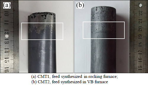
Fig. 1 As-grown CMT crystal ingots by THM with different conditions of polycrystalline feed
In order to study the interface morphologies in details, the CMT slice with the thickness of 2.5 mm near the Te-rich solvent zone was cut along the growth direction. Figure 2 shows the typical cross-sections view of the growth interface and the corresponding wafer cut along the radial direction just below the interfaces. It was found that a flat or slightly convex growth interface was more in favor for single crystals growth, but the two growth interfaces obtained from our ingots were both concave. In Fig. 2(a), the growth interface of CMT1 was irregular concave, with the curvature [14] (d=h/r) of about 0.34. The black region below the interface was the grown crystal and the bright region above the interface with dendrite structure was the Te-rich solvent zone. The growth interface of CMT2 as shown in Fig. 2(b) was symmetrical with the curvature of about 0.17. By comparing the corresponding wafer below the interfaces, shown in Figs. 2(c) and (d), the wafer from CMT2 had larger grains and less grain boundaries. Since the growth parameters of both crystals were constant, the difference of the growth interface between CMT1 and CMT2 could be due to the different states of polycrystalline feed materials. The polycrystalline feed material synthesized by VB method results in uniform composition and size distribution of the CMT polycrystalline. In Fig. 2(a) and Fig. 2(b), it is found that the size and distribution of the dendrite structure CMT crystal particle in the Te-rich solvent were more uniform in CMT2 as compared to CMT1.
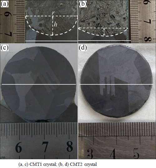
Fig. 2 Cross-sections of growth interface and corresponding CMT wafer below interfaces
The typical IR transmission images of the whole growth interface are shown in Fig. 3. The bright portions were the as-grown CMT, while the black regions were the Te-rich solvent, and the interface shapes in CMT1 and CMT2 were clearly revealed. Be similar with the cross-section pictures under optical microscope, the IR images also showed that the growth interfaces were irregular concave which were due to the undesirable growth parameters as mentioned above. Furthermore, it can be seen clearly from Fig. 3 that the interfaces were not symmetrical along the radial direction of the slice, which may be resulted by the local heat and melt convection perturbations as well as the interactions between ampoule and melt [15].
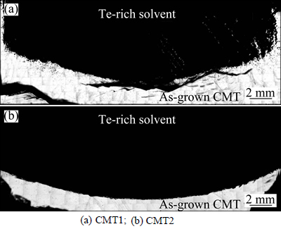
Fig. 3 IR transmission images of growth interfaces
It is worth mentioning that the Te inclusion had detrimental effects on the device performance [16,17]. From the investigation by ROY et al [9], the main formation mechanism of Te inclusion in THM technique was the trapping of the Te-rich solution at the irregular growth interface. So, it was possible to reduce the Te inclusion density by improving the growth interface morphology. Figure 4 shows the left edges of the two interfaces and the magnified version of corresponding region. It was clear from Fig. 4(a) that the CMT1 crystal near the ampoule inner wall grew more quickly than the middle region, which resulted in a more concave growth interface as compared to CMT2 shown in Fig. 4(b). Figure 4(c) shows the magnified version of corresponding red-box regions in Fig. 4(a) which clearly demonstrated the process of the formation of Te- inclusion. Some uncontrolled growth fronts grew more quickly than other fronts near the interface, which would touch each other or form a so-called ��back-growth�� [18], and trapped some Te-rich solution to form the Te inclusion eventually. Obviously, the rougher the growth interface was, the more and larger the Te inclusions could be formed. Compared with CMT1 in Fig. 4(c), the interface of CMT2 in Fig. 4(d) from VB synthesized polycrystalline feed revealed lower roughness, and there were less and smaller Te inclusions in CMT2 crystal. The polycrystalline feed material synthesized by VB technique in CMT2 resulted in uniform solute distribution along the growth interface, which was beneficial for a relatively smooth growth interface and decrease of Te inclusions.
Figure 5 shows the middle region of the growth interface. Theoretically, the convection flows did not reach the center of ingot due to the lower heat conductivity and the associated structure of the melt of CMT crystal, therefore, the growth interface shape at the middle region should be smooth and flat approximately [15]. The middle region of the growth interface of CMT2 shown in Fig. 5(b) had exactly proved the viewpoint mentioned above. However, the middle region of the growth interface of CMT1 shown in Fig. 5(a) was unstable and fluctuated, due to the non-uniform composition distribution of polycrystalline feed and the unstable transport of solute in the Te-rich solvent zone.
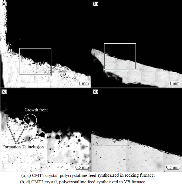
Fig. 4 Morphology of interface in left edges and magnified version of corresponding region
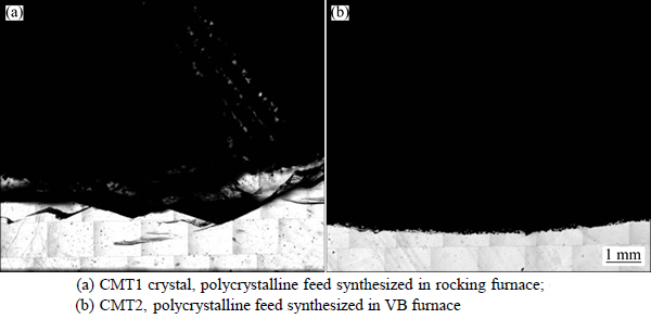
Fig. 5 Morphology of interface in middle region
The Mn composition distributions along the radial direction of the CMT wafers just below the growth interface shown in Fig. 2 were measured by EDS. As shown in Fig. 6, the Mn concentrations of both CMT wafers decreased from center to periphery. Since the growth interface was concave and the segregation coefficient of Mn was less than unit [19], the center has the highest Mn concentration and the periphery has the lowest one. Moreover, the Mn concentration difference along the radial direction of the CMT1 was about 1.2% which was obviously higher than 0.6% of the CMT2. This is related to the curvature of the concave growth interface closely.
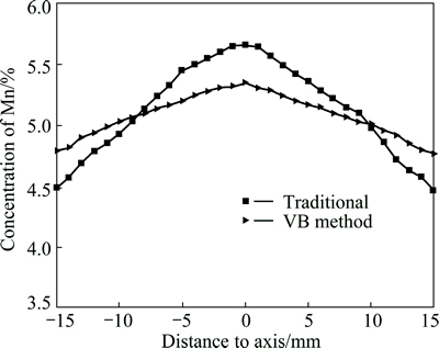
Fig. 6 Mn composition distributions along radial direction of CMT1 and CMT2 wafers below growth interface
3.3 Te inclusion
The Te inclusions in the CMT wafers cut below the interfaces of the ingots were evaluated by the IR transmission microscopy, as shown in Fig. 7. Table 1 summarized the statistical numbers of Te inclusions in CMT1 and CMT2. The size of Te inclusions in CMT1 wafer was 8-20 ��m and the density was in the range of 1.7'105-4.2'105 cm-3, while the size of Te inclusions in CMT2 was 4-16 ��m and the density was in the range of 8.6'104-1.5'105 cm-3. It is found that the CMT2 crystal has smaller and less Te inclusions as compared to the CMT1 crystal. The reason is that the growth interface of the CMT2 crystal is relatively smooth with low curvature d of 0.17, which significantly reduces the formation of Te inclusions. In addition, the concentration distributions of Te inclusion along the radial direction of each wafer (the white line shown in Figs. 2(c) and (d)) were shown in Fig. 8. The density difference of Te inclusions between the peripheral part and the middle part of the CMT1 wafer is larger compared with that of CMT2 wafer, which is correlated to the curvature of growth interface of CMT crystal. Both CMT wafers had low density of Te inclusion in the middle parts, since the middle region had a stable and smooth growth interface. Therefore, a smooth growth interface with low curvature is beneficial for decreasing Te inclusions during THM growth.
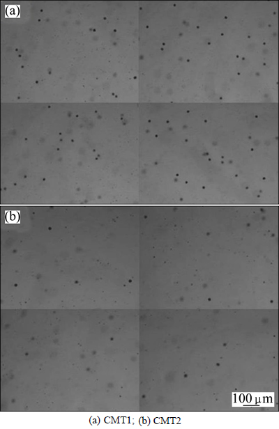
Fig. 7 Typical morphology of Te inclusion
Table 1 Comparison of size and density of Te inclusion in CMT1 and CMT2 wafers
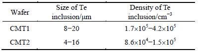
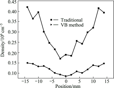
Fig. 8 Density distribution of Te inclusion along radial direction of CMT1 and CMT2 wafers
4 Conclusions
1) The growth interfaces of CMT crystals grown by the THM technique with the CMT polycrystalline feed synthesized in a rocking furnace and vertical Bridgman furnace were investigated.
2) The states of polycrystalline feeds have effects on the concave growth interface, and the curvatures (d=h/r) of the growth interface in CMT1 and CMT2 were about 0.34 and 0.17, respectively.
3) The Mn concentrations segregation along the radial direction of CMT1 was about 1.2% which was obviously higher than 0.6% of the CMT2.
4) The size of Te inclusions in CMT1 wafer was 8-20 ��m and the density was in the range of 1.7'105-4.2'105 cm-3, while the size of Te inclusions in CMT2 was 4-16 ��m and the density was in the range of 8.6'104-1.5'105 cm-3.
5) The results show that a smooth growth interface with low curvature is obtained from the feed synthesized in vertical Bridgman furnace, which is beneficial for decreasing the Mn composition segregation and Te inclusions in CMT crystals grown by THM technique.
References
[1] KIM K H, JENG G, KIM P, CHOI J, Bolotnikov A E, Camarda G S, James R B. Influence of the cooling scheme on the performance and presence of carrier traps for CdMnTe detectors [J]. Journal of Applied Physics, 2013, 114(6): 063706.
[2] Rafiei R, Reinhard M, Kim K, Prokopovich D, Boardman D, Sarbutt A, James R B. High-purity CdMnTe radiation detectors: A high-resolution spectroscopic evaluation [J]. IEEE Transactions on Nuclear Science, 2013, 60(2): 1450-1456.
[3] Hossain A, Cui Y, Bolotnikov A E, Camarda G S, Yang G, Kochanowska D, James R B. Vanadium-doped cadmium manganese telluride (Cd1-xMnxTe) crystals as X-and gamma-ray detectors [J]. Journal of Electronic Materials, 2009, 38(8): 1593-1599.
[4] Du Yuan-yuan, Jie Wan-qi, Wang Tao, Luo Lin, Xu Ya-dong, Luan Li-jun. Study on twin boundaries and Te particles in CdMnTe crystals for nuclear detector application [J]. Journal of Crystal Growth, 2013, 364: 128-132.
[5] WANG Tao, JIE Wan-qi, XU Ya-dong, ZHA Gang-qiang, FU Li. Characterization of CdZnTe crystal grown by bottom-seeded Bridgman and Bridgman accelerated crucible rotation techniques [J]. Transactions of Nonferrous Metals Society of China, 2009, 19(S): s622-s625.
[6] Wei Gao-li, Wang Lin-jun, Zhang Ji-jun, Yuan Zhen-wen, Qin Kai-feng, Min Jia-hua, Liang Xiao-yan, Xia Yi-ben. Growth and characterization of indium-doped Cd1-xZnxTe crystal by traveling heater method [J]. Nuclear Instruments and Methods in Physics Research Section A: Accelerators, Spectrometers, Detectors and Associated Equipment, 2013, 704: 127-130.
[7] Liu Y, Dost S, Lent B, Redden R F. A three-dimensional numerical simulation model for the growth of CdTe single crystals by the travelling heater method under magnetic field [J]. Journal of Crystal Growth, 2003, 254(3): 285-297.
[8] Xu Ya-dong, Liu Hang, He Yi-hui, Yang Rui, Luo Lin, Jie Wan-qi. Research into the electrical property variation of un-doped CdTe and ZnTe crystals grown under Te-rich conditions [J]. Journal of Alloys and Compounds, 2014, 612: 392-397.
[9] Roy U N, Weiler S, Stein J. Growth and interface study of 2-in diameter CdZnTe by THM technique [J]. Journal of Crystal Growth, 2010, 312(19): 2840-2845.
[10] Triboulet R. The travelling heater method (THM) for Hg1-xCdxTe and related material [J]. Progress in Crystal Growth and Characterization of Materials, 1994, 28(1): 85-144.
[11] Roy U N, Weiler S, Stein J. Macro-and microscopic growth interface study of CdZnTe ingots by THM technique [C]//SPIE Optical Engineering+ Applications. California, San Diego: International Society for Optics and Photonics, 2010: 780502.
[12] Wang Y, Kudo K, Inatomi Y, Ji R B, Motegi T. Growth interface of CdZnTe grown from Te solution with THM technique under static magnetic field [J]. Journal of Crystal Growth, 2005, 284(3): 406-411.
[13] Du Yuan-yuan, Jie Wan-qi, Wang Tao, Zheng Xin, Xu Ya-dong, Luan Li-jun. Solution growth of In-doped CdMnTe crystals by the vertical Bridgman method with the ACRT technique [J]. Journal of Crystal Growth, 2012, 355(1): 33-37.
[14] Rudolph P. Fundamental studies on bridgman growth of CdTe [J]. Progress in Crystal Growth and Characterization of Materials, 1994, 29(1): 275-381.
[15] Datta A, Swain S, Bhaladhare S, Kelvin G L. Experimental studies on control of growth interface in MVB grown CdZnTe and its consequences [C]//Nuclear Science Symposium and Medical Imaging Conference, 2011. Valencia: IEEE, 2011: 4720-4726.
[16] NAN Rui hua, JIE Wan qi, ZHA Gang qiang, BAI Xu-xu, WANG Bei, YU Hui. Determination of trap levels in CZT: In by thermally stimulated current spectroscopy [J]. Transactions of Nonferrous Metals Society of China, 2012, 22(S1): s148-s152.
[17] Bolotnikov A E, Camarda G S, Carini G A, Cui Y, Li L, James R B. Cumulative effects of Te precipitates in CdZnTe radiation detectors [J]. Nuclear Instruments and Methods in Physics Research Section A: Accelerators, Spectrometers, Detectors and Associated Equipment, 2007, 571(3): 687-698.
[18] DU Yuan-yuan, JIE Wan-qi, ZHENG Xin, WANG Tao, BAI Xu-xu, YU Hui. Growth interface of In-doped CdMnTe from Te solution with vertical Bridgman method under ACRT technique [J]. Transactions of Nonferrous Metals Society of China, 2012, 22(S1): s143-s147.
[19] Yang G, Bolotnikov A E, Li L, Camarda G S, Cui Y, Hossain A, James R B. Investigation of cadmium manganese telluride crystals for room-temperature radiation detection [J]. Journal of Electronic Materials, 2010, 39(7): 1053-1057.
�ƶ�������������CdMnTe�������������
�����䣬�ż̾������־����ɼλ�������������С�࣬�� ������ ��
�Ϻ���ѧ ���Ͽ�ѧ�빤��ѧԺ���Ϻ� 200444
ժ Ҫ���о����ƶ�������������CdMnTe������������档���ô�ͳҡ��¯�ʹ�ֱBridgman¯�ϳɶྦྷԭ�ϣ����Ƚ��˲�ͬ�ྦྷԭ�϶��ƶ������������������Ӱ�졣�����ʾ�����ô�ֱBridgman���ϳɶྦྷ������CdMnTe����(CMT2)����ڴ�ͳҡ��¯�ϳɶྦྷ�����ľ���(CMT1)�������������Ϊ�⻬�Ұ������ʸ��͡����������������CdMnTe�����Mn�ɷֺ�Te������ֲ���Ӱ�졣CMT2����Mn�ľ���ɷַ�����Te�������ܶȼ��ߴ��С��CMT1���塣��֮����ֱBridgman���ϳɶྦྷԭ�������Ը��������������̬�������ڽ����ƶ�������������CdMnTe�����Te�������Mn�ijɷַ�������߾����������
�ؼ��ʣ�CdMnTe���ƶ������������������棻�ྦྷԭ��
(Edited by Yun-bin HE)
Foundation item: Projects (11375112, 51472155, 11275122) supported by the National Natural Science Foundation of China
Corresponding author: Ji-jun ZHANG; Tel: +86-21-66136126; E-mail: zhangjijun222@shu.edu.cn
DOI: 10.1016/S1003-6326(16)64248-6
Abstract: The growth interfaces of CdMnTe (CMT) crystals grown by traveling heater method (THM) were studied. Two types of polycrystalline CMT feed ingots synthesized in a traditional rocking furnace and vertical Bridgman (VB) furnace were adopted in THM growth, and the effects of the polycrystalline feed on the growth interface were revealed. The morphology of the growth interface of CMT crystal (CMT2) grown from the feed by vertical Bridgman was smoother with lower curvature compared with that of CMT crystal (CMT1) from the feed by rocking furnace. The radial Mn composition and Te inclusion distribution of the CMT wafers were analyzed and correlated to the growth interface. The Mn segregation along the radial direction and Te inclusion density of CMT2 were lower than those of CMT1. The VB method synthesized polycrystalline feed could improve the growth interface morphology, which is beneficial for decreasing the Te inclusions and Mn segregation in CMT wafers.
