

![]()

Trans. Nonferrous Met. Soc. China 22(2012) 2548-2553
Preparation, microstructure and dislocation of solar-grade multicrystalline silicon by directional solidification from metallurgical-grade silicon
SU Hai-jun, ZHANG Jun, LIU Lin, FU Heng-zhi
State Key Laboratory of Solidification Processing, Northwestern Polytechnical University, Xi��an 710072, China
Received 9 July 2012; accepted 3 September 2012
Abstract:
A vacuum directional solidification with high temperature gradient was performed to prepare low cost solar-grade multicrystalline silicon (mc-Si) directly from metallurgical-grade mc-Si. The microstructure characteristic, grain size, boundary, solid-liquid growth interface, and dislocation structure under different growth conditions were studied. The results show that directionally solidified multicrystalline silicon rods with high density and orientation can be obtained when the solidification rate is below 60 ��m/s. The grain size gradually decreases with increasing the solidification rate. The control of obtaining planar solid-liquid interface at high temperature gradient is effective to produce well-aligned columnar grains along the solidification direction. The growth step and twin boundaries are preferred to form in the microstructure due to the faceted growth characteristic of mc-Si. The dislocation distribution is inhomogeneous within crystals and the dislocation density increases with the increase of solidification rate. Furthermore, the crystal growth behavior and dislocation formation mechanism of mc-Si were discussed.
Key words:
multi-crystalline silicon; metallurgical-grade silicon; silicon solar cell; directional solidification; microstructure;
1 Introduction
With the rapid development of modern industry, the energy demand of global world is greatly increased annually; however, conventional energies such as coal, petroleum and natural gas are non-renewable and severely pollute the environment [1]. Silicon solar cell has become the dominant energy material used in the photovoltaic (PV) industry field for solving energy and environmental problems worldwide [2,3].
At present, over 95% of commercial solar cells are made by using crystalline silicon [4]. The current share ratio of multicrystalline silicon (mc-Si) wafer is over 50% in the silicon solar cell market and the annual production is more than 10 GW [5]. The conversion efficiency of mc-Si reaches 20.3%, which is almost near to that of single crystalline silicon (sc-Si) [3,6]. However, as compared with conventional energy materials, the major limitation to wide practice application of silicon solar cell is its high cost, in which silicon wafer occupies 40%-60%. The present raw materials of mc-Si solar cell mainly come from the head-end materials or scraps of sc-Si used in the micro-electronic industry, the cost of which is high in comparison with metallurgical-grade mc-Si and a large shortage of which is gradually faced with increasing expectations for the solar cell market. Moreover, the dominant preparation technique of mc-Si is still the improved Siemens method, which severely pollutes environment.
Recently, the mc-Si grown based on the directional solidification has attracted great attention due to its low production cost, low energy consumption, low pollution and high throughput [7-10]. Furthermore, by exactly controlling thermal flow along the growth direction, well aligned columnar crystals with good orientations can be obtained. However, most previous studies about solar-grade Si were mainly focused on the purification effect of mc-Si by directional solidification, and the preparation was mainly conducted at a low growth rate and metallurgical-grade mc-Si with a low purity was less used as raw materials [11-15]. In this work, the solar- grade mc-Si was directly prepared from metallurgical-grade mc-Si. The microstructure evolution, solid-liquid interface and dislocation structure under different growth conditions were investigated, and the growth mechanism of mc-Si crystal at a high temperature gradient was discussed.
2 Experimental
The starting feedstock materials were commercial metallurgical-grade mc-Si ingots with purity of higher than 99.5%. Cylindrical mc-Si precursor rods with a diameter of 6 mm and a length of 80 mm were cut from the original ingot using diamond-cutting machine and cleaned using acetone and alcohol. Then, the obtained rod samples were inserted in a matched high purity quartz crucible to start directional solidification. When the vacuum of the furnace chamber was pumped up to 5��10-2 Pa, the samples were inductively remelted and solidified in a high thermal gradient Bridgman directional solidification furnace under high purity argon atmosphere. After being heated to stabilization at 1450 �� for 30 min, the sample was pulled downward through the furnace at a constant velocity (5-60 ��m/s). At the end of the experiment, the samples were quenched by pulling them rapidly into the Ga-In-Sn liquid metal bath to obtain the solid-liquid interface. A type-B thermocouple (Pt-6%Rh/Pt-30%Rh) was used to measure the melt temperature at different rates. The temperature gradient was about 200 K/cm.
The directionally solidified samples were cut along longitudinal and transverse cross-sections, and then ground and polished with standard metallographic techniques. To reveal the microstructure and dislocation, the specimens were etched with an etching solution of V(HF):V(HNO3)=1:1 for 5 s and then characterized by an optical microscope (Leica, DM4000M). The chemical composition of the solidified sample was analyzed by inductively coupled plasma atomic emission spectrometry (ICP-AES).
3 Results and discussion
3.1 Solid-liquid interface morphology and micro- structure characteristics
The morphology control of the solid-liquid interface during unidirectional growth processes is the key to obtain high quality crystals [16], which is generally determined by the temperature gradient and growth velocity. Figure 1 shows the typical solid-liquid interface morphology of directionally solidified mc-Si grown at the rate of 5 ��m/s. At the middle part of the rod sample (Fig. 1(a)), the solid-liquid interface presents a flat growth morphology. In the solidified zone, the
dendrite Si crystals directionally grow along the growth directions at the initial growth stage, as shown by the dark arrows. The dendrite Si crystals generally grow much faster than the equiaxed grains, so the dendrite grains could be much larger [5]. The grains near the interface are fine, and the sizes gradually increase with the increase of the distance away from the interface, namely, the grain sizes increase with the height in the solidified crystal. Similar results are also found by FUJIWARA et al [17], in which the dendrite growth along the crucible bottom wall is obtained by controlling the cooling rate at the initial stage of directional solidification. Moreover, the solidified zone is dense and no obvious casting defects are found, which is different from the conventional directional solidification ingot [18]. However, in the quenched liquid zone, there are many defects formed such as pores shown by the white arrows, and the crystals grow with the random orientation. The planar growth front morphology obtained is mainly ascribed to the high temperature gradient that can enhance the stability of the melt growth interface. At the edge part of the rod sample (Fig. 1(b)), the solid-liquid interface slightly convexes towards the liquid, as shown by the dashed line, which may primarily be caused by the side thermal radiation in the radial direction. As a result, the grains grow outward from the inner shown by the dark arrow, and the grain size in average is smaller in the side wall than that of the inner of the sample.
Figure 2 shows the microstructures of longitudinal cross-sections of the directionally solidified mc-Si rods at different parts grown at the rate of 5 ��m/s. As shown, at the stable growth stage of the middle part (Fig. 2(a)), well-aligned columnar silicon crystals are produced with orientation approximately parallel to the growth direction. The parallel grain boundaries can be clearly observed as shown by the dark arrows, and there are almost no transverse grain boundaries. Moreover, it is noted that the grain size distribution is not uniform within individual grains such as grains A and D. At the top part (Fig. 2(b)), the grains grow completely in the perpendicular direction, which is superior to that of the middle part possibly caused by the axial radiation at the top. Only a few lateral grain boundaries can be seen, as shown by the white arrows in Fig. 2(b). Generally, the silicon crystals prefer to grow with a faceted solidification interface and crystallization feature, which results in the fact that the growth directions of the silicon columnar crystals are not as straight as that of metals [15]. The columnar grains and straight grain boundaries growing parallel to the heat flux direction mean that the solidification occurs directionally and the planar growth front interface is produced, which agrees with the solid-liquid interface result in Fig. 1. Although the raw materials are metallurgical-grade mc-Si with high impurities, no precipitate is observed at the grain boundaries in the whole sample grown at a low rate, which indicates that the directional solidification with high temperature gradient can improve the solidification microstructures in comparison with conventional directionally solidified silicon, and will be beneficial to improving the properties of mc-Si. However, the directional growth is weakened in the outermost region of the sample, where the grains tend to slightly incline in the radial direction, as shown in Fig. 2(c). Many lateral grain boundaries (dark arrows) are found and some stacking faults form (white arrows). This indicates that preventing the radial thermal radiation during the directional solidification process is important to improve the solidification microstructure of mc-Si.

Fig. 1 Solid-liquid interface morphologies of directionally solidified mc-Si sample: (a) Middle zone; (b) Edge zone
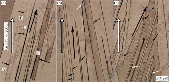
Fig. 2 Microstructures of longitudinal cross-sections of different growth regions for directionally solidified mc-Si rods grown at rate of 5 ��m/s: (a) Middle part; (b) Top part; (c) Edge part
Figure 3 shows the microstructure evolution of directionally solidified mc-Si grown at different solidification rates. Obviously, the size of Si grain is fine in comparison with the conventional directional solidification of Si [19] due to the high temperature gradient that leads to rapid cooling rate. Neither dendritic nor cellular structure is found in the samples. In this directional solidification system, the temperature gradient is about 200 K/cm, which is far higher than that of the conventional directional solidification equipment. According to the nucleation theory, the crystal nucleation is derived by a certain undercooling. A higher cooling rate prefers to produce a higher undercooling and nucleation rate. Thus, when the temperature gradient is kept constant, increasing the solidification rate will lead to the increase of nucleation rate of columnar grains and, consequently forming finer crystals, as shown in Fig. 3. As the solidification rate increases from 5 to 60 ��m/s, the average size of the columnar grain decreases from 200 to 20 ��m, and the columnar grain keeps the directional growth orientation parallel to the thermal flow direction even at high growth rate, which indicates that the high temperature gradient can enhance the growth stability of Si crystal and obtain well aligned columnar grains. Furthermore, some small precipitates are also observed in the partial zone of the solidified sample at rate of 60 ��m/s, as shown in Fig. 4. Similar results are also found by MARTORANO et al [9]. Because silicon grows with a faceted characteristic and strong anisotropy, the growth interface is unstable. At high rate, the low impurities in raw materials tend to enrich at the growth interface front, which will result in the constitutional undercooling and destroy the planar solid-liquid interface, and consequently, producing precipitates.

Fig. 3 Microstructure evolution of directionally solidified mc-Si grown at different rates: (a) 10 ��m/s; (b) 20 ��m/s; (c) 40 ��m/s; (d) 60 ��m/s

Fig. 4 Precipitates in directionally solidified mc-Si
3.2 Dislocation characteristic
Dislocations are considered to be important defects commonly formed in the mc-Si, and extremely affect the properties of materials. For example, the high dislocation densities in local regions are known to be detrimental to minority carrier lifetime [12]. Therefore, understanding the dislocation and twin boundary characteristics is necessary to control the formation of defects. Figure 5(a) shows the typical dislocation structure in the sample grown at rate of 5 ��m/s. The distribution of dislocations is highly inhomogeneous among the grains, and the average dislocation density is about 1?105 cm-2. The dislocations are arrayed in the form of dislocation cluster, showing a typical slip dislocation characteristic, which is similar to the result of CHEN et al [8]. Moreover, the twin boundary with step growth originated from a grain boundary is clearly observed as the arrows shown in Fig. 5(b). It is suggested that the twin boundaries are generally generated from a normal grain boundary during the directional growth process, which are mainly caused by faceted growth habit of Si melt at the solid-liquid interface front [20].

Fig. 5 Dislocation (a) and twin boundary (b) in directionally solidified mc-Si grown at rate of 5 ��m/s
Figure 6 shows the dislocation distribution in the mc-Si sample grown at the rate of 20 ��m/s. The dislocations primarily consist of slip dislocations, and the dislocation distribution is also very inhomogeneous, but the density increases obviously in comparison with Fig. 5.
The slip dislocation is considered to be the formation reason of the inhomogeneous dislocation distribution [5]. In Fig. 6(a), it can be seen that the dislocation is produced from a triple-grain junction (A, B and C), as shown by the arrows, which further indicates that the generation of crystal defects, such as dislocations or twin boundaries, is highly related to the grain boundary. The increase of the dislocation distribution is mainly caused by the increased cool rate under rapid solidification conditions, which produces larger stress. The stress given to the grain boundary will lead to increasing defect generation.

Fig. 6 Dislocation distribution in directionally solidified mc-Si grown at rate of 20 ��m/s: (a) Dislocation produced from grain junction; (b) Dislocation produced from grain boundary
4 Conclusions
1) The directional solidification with high temperature gradient is applied to preparing solar-grade mc-Si directly from metallurgical-grade mc-Si. By obtaining the planar solidification interface, well-aligned columnar grains with high orientation parallel to the growth direction are obtained at the rate of 5-60 ��m/s.
2) The grain size decreases with increasing the solidification rate, and only a few precipitates are observed at high solidification rate due to the interface instability caused by the constitutional undercooling.
3) High density slip dislocations with inhomogeneous distribution form in the directionally solidified mc-Si. The dislocations and twin boundaries tend to produce from the boundary, and the density decreases with the increase of the solidification rate.
References
[1] SUGANTHI L, SAMUEL A A. Energy models for demand forecasting��A review [J]. Renew Sust Energ Rev, 2012, 16(2): 1223-1240.
[2] WU H J, MA W H, CHEN X H, JIANG Y, MEI X Y, ZHANG C, WU X H. Effect of thermal annealing on defects of upgraded metallurgical grade silicon [J]. Transaction of Nonferrous Metals Society of China, 2011, 21(6): 1340-1347.
[3] Su H J, Zhang J, Liu L, Fu H Z. Preparation development of high-quality solar-grade multi-crystalline silicon by directional solidification [J]. Adv Mater Res, 2011, 311-313: 1389-1392.
[4] YAHI I S, YAKUPHANOGLU F, AZIM O A. Unusual photocapacitance properties of a mono-crystalline silicon solar cell for optoelectronic applications [J]. Sol Energy Mater Sol Cells, 2011, 95(9): 2598-2605.
[5] SCHMID E, W?RZNER S, FUNKE C, GALNDO V, P?TZOLD O, STELTER M. The effect of the growth rate on the microstructure of multi-crystalline silicon [J]. J Cryst Growth, 2012, 359(1): 77-82.
[6] LI X Q, YANG D R, YU X G, QUE D L. Precipitation and gettering behaviors of copper in multicrystalline silicon used for solar cells [J]. Transaction of Nonferrous Metals Society of China, 2011, 21(3): 691-696.
[7] MORITA K, YOSHIKAWA T. Thermodynamic evaluation of new metallurgical refining processes for SOG-silicon production [J]. Transaction of Nonferrous Metals Society of China, 2011, 21(3): 685-690.
[8] CHEN N, QIU S Y, LIU B F, DU G P, LIU G H, SUN W. An optical microscopy study of dislocations in multicrystalline silicon grown by directional solidification method [J]. Mat Sci Semicond Process, 2010, 13(4): 276-280.
[9] MARTORANO M A, FERREIRA NETO J B, OLIVEIRA T S, TSUBAKI T O. Refining of metallurgical silicon by directional solidification [J]. Mater Sci Eng B, 2011, 176(3): 217-226.
[10] BAIRAVA G R, RYNINGEN B, SYVERTSEN M, ?VRELID E, SAHA I, TATHGAR H, RAJESWARAN G. Growth and characterization of multicrystalline silicon ingots by directional solidification for solar cell applications [J]. Energy Procedia, 2011, 8: 371-376.
[11] LUO D W, LIU N, LU Y P, ZHANG G L, LI T J. Removal of boron from metallurgical grade silicon by electromagnetic induction slag melting [J]. Transaction of Nonferrous Metals Society of China, 2011, 21(5): 1178-1184.
[12] RYNINGEN B, STOKKAN G, KIVAMBE M, ERVIK T, LOHNE O. Growth of dislocation clusters during directional solidification of multicrystalline silicon ingots [J]. Acta Mater, 2011, 59(20): 7703-7710.
[13] GREGORI N J, MURPHY J D, SYKES J M, WILSHAW P R. Chemical etching to dissolve dislocation cores in multicrystalline silicon [J]. Physical B, 2012, 407(15): 2970-2973.
[14] LI T F, HUANG H C, TSAI H W, LAN A, CHUCK C, LAN C W. An enhanced cooling design in directional solidification for high quality multi-crystalline solar silicon [J]. J Cryst Growth, 2012, 340(1): 202-208.
[15] FUJIWARA K. Crystal growth behaviors of silicon during melt growth processes [J]. Inter J Photoenergy, 2012, 2012: 1-16.
[16] MA X, ZHENG L L, ZHANG H, ZHAO B, WANG C, XU F H. Thermal system design and optimization of an industrial silicon directional solidification system [J]. J Cryst Growth, 2011, 318(1): 288-292.
[17] FUJIWARA K, PAN W, SAWADA K, TOKAIRIN M, USAMI N, NOSE Y, NOMURA A, SHISHIDO T, NAKAJIMA K. Directional growth method to obtain high quality polycrystalline silicon from its melt [J]. J Cryst Growth, 2006, 292(2): 282-285.
[18] DU G P, CHEN N, ROSSETTO P. On-wafer investigation of SiC and Si3N4 inclusions in multicrystalline Si grown by directional solidification [J]. Sol Energy Mater Sol Cells, 2008, 92: 1059-1066.
[19] KIM D L, KIM T K. Characteristics of structural defects in the 240 kg silicon ingot grown by directional solidification process [J]. Sol Energy Mater Sol Cells, 2006, 90(11): 1666-1672.
[20] CUI C J, ZHANG J, SU H J, LIU L, FU H Z. Growth mechanism of the directionally solidified Si-TaSi2 eutectic in situ composite [J]. J Cryst Growth, 2009, 311(8): 2555-2559.
ұ��趨�����̷��Ʊ�̫���ܼ��ྦྷ�輰������֯��λ��
�պ������� ������ �֣�����־
������ҵ��ѧ ���̼��������ص�ʵ���ң����� 710072
ժ Ҫ����ұ���Ϊԭ�ϣ�̽�����þ��и��¶��ݶȵ���ն������̼����Ʊ��ͳɱ�̫���ܼ��ྦྷ�裬���о����ڲ�ͬ���������µ�����֯�����������뾧����С����Һ������ò�Լ�λ���ṹ��������������������ʵ���60 ��m/s ʱ���ܻ�þ��и��ܶȺ�����ȡ��Ķ������̶ྦྷ���״�������辧����С���������ʵ��������С���ڿ������̹��̣����ƽ�Ĺ�Һ������ò�ǻ�������̷���������״���Ĺؼ������ڹ��Сƽ���������ԣ�����֯�г�����λ������̨���Ͼ��ṹ���ھ����У�λ���ֲ����ֲ������ԣ�����λ���ܶ����������ʵ����Ӷ����ӣ��ڴ˻����ϣ������˶ྦྷ���������Ϊ�Լ�λ���γɻ��ơ�
�ؼ��ʣ��ྦྷ�裻ұ�裻̫���ܵ�أ��������̣�����֯
(Edited by CHEN Wei-ping)
Foundation item: Projects (51002122, 51272211) supported by the National Natural Science Foundation of China; Project (2010ZF53064) supported by the Aeronautical Science Foundation of China; Project (2012M51028) supported by the Postdoctoral Science Foundation of China; Project (2010JQ6005) supported by the Natural Science Foundation of Shaanxi Province, China; Project (76-QP-2011) supported by the Research Fund of State Key Laboratory of Solidification Processing in NWPU, China; Project (B08040) supported by the 111 Project, China
Corresponding author: SU Hai-jun; Tel: +86-29-88492228; E-mail: shjnpu@yahoo.com.cn
DOI: 10.1016/S1003-6326(11)61499-4
Abstract: A vacuum directional solidification with high temperature gradient was performed to prepare low cost solar-grade multicrystalline silicon (mc-Si) directly from metallurgical-grade mc-Si. The microstructure characteristic, grain size, boundary, solid-liquid growth interface, and dislocation structure under different growth conditions were studied. The results show that directionally solidified multicrystalline silicon rods with high density and orientation can be obtained when the solidification rate is below 60 ��m/s. The grain size gradually decreases with increasing the solidification rate. The control of obtaining planar solid-liquid interface at high temperature gradient is effective to produce well-aligned columnar grains along the solidification direction. The growth step and twin boundaries are preferred to form in the microstructure due to the faceted growth characteristic of mc-Si. The dislocation distribution is inhomogeneous within crystals and the dislocation density increases with the increase of solidification rate. Furthermore, the crystal growth behavior and dislocation formation mechanism of mc-Si were discussed.
