
DOI�� 10.11817/j.issn.1672-7207.2020.09.013
�첽�Գ�˫դInGaZnO��Ĥ����ܱ�����ƵĽ���ģ��
������1��������1, 2������Ӫ1������1���δ�ά1����1, 2��������1
(1. ���ϴ�ѧ ���������ѧԺ������ ��ɳ��410083��
2. ����ʡ����Ƭʽ��м��Ƚ�����װ�����̼����о����ģ����� ������419600)
ժ Ҫ��
դ�ṹ����������п(InGaZnO)��Ĥ�����(thin film transistors��TFTs)����Ⲵ�ɷ��̣�������������������������ͨ���IJ�ͬ�ֲ��ص㣬�������������Чƽ����ѹ�ĸ���ڵ�ͨ������Lambert W�������ƣ������첽�Գ�˫դInGaZnO TFT������ƽ���ģ�͡���ģ�͵���ϲ���ֻ��2�����ܹ��Ϻõط�ӳ�����ȡ�������ѹ�Ȳ����Ե��Ƶ�Ӱ�졣��������ģ�ͼ�TCAD�������о�InGaZnO���ȡ�դ���ʲ����Լ�ȱ��̬�ܶȵ��������Զ���դ��˫դ����ܱ�����Ƶ�Ӱ�졣�о������������������������������ŵ�դ��ѹ����ʽ��������������ڶ�դ��ѹ����������ƽ�ƣ��ڵ�ͨ��������������ŵ�դ��ѹ���������ͣ��ҵ���ֵ�붥դ���Ƶ�ѹ������ض�С��������ƵĽ���ģ����TCAD��ֵ�������Աȣ����нϸߵ��Ǻ϶ȣ��ڲ�ͬȱ��̬�ܶȷֲ�����£�����ģ�͵ļ���ֵ��TCAD����ֵ�������С��10%�����о��ɹ��������˽�˫դInGaZnO TFT�ĵ�ͨ���ƣ�������InGaZnO TFT��������ģ����ؼ��ɵ�·��ơ�
�ؼ��ʣ�
˫դ��Ĥ�������������������ģ��������п��������
��ͼ����ţ�O47 ���ױ�־�룺A
���±�ţ�1672-7207��2020��09-2480-09
Surface potential model for amorphous InGaZnO thin-film transistors with independent symmetric double-gate
HE��Yini1, DENG��Lianwen1, 2, ZHEN��Liying1, QIN��Ting1, LIAO��Congwei1, LUO��Heng1, 2,HUANG��Shengxiang1
(1. School of Physics and Electronics, Central South University, Changsha 410083, China;
2. Engineering Technology Research Center in Novel Chip Inductance and Advanced Manufacturing Equipment of Hunan Province, Huaihua 419600, China)
Abstract: An analytical surface potential model for the independent symmetric double-gate InGaZnO TFTs(thin film transistors) was presented.The Poisson equation was solved according to the different carrier density distributions in the subthreshold and conduction region. In the subthreshold region, the concept of equivalent flat band voltage was introduced, and in the conduction region, the approximated Lambert W function was applied to develop the analytical surface potential model for the amorphous InGaZnO thin-film transistors with independent symmetric double-gate. Furthermore, the effects of the different oxide thickness, the active layer thickness and the density of defect states were discussed. The results show that, in the subthreshold region, the surface potential increases approximately linearly with the increase of the bottom grid voltage, the surface potential shifts during the top-gate voltage modulation. In the conduction region, the surface potential has few correlation with the top-gate voltage. The present potential model shows excellent agreement with the simulation values. In the case of different densities of state distribution, the relative error of the calculation model and the TCAD analysis value is less than 10%. The result is helpful to understand the conduction mechanism of the InGaZnO TFTs, and is useful for the InGaZnO TFT device simulation and the related integrated circuit design.
Key words: independent double-gate TFTs(thin film transistors); surface potential; analytical model; InGaZnO
���������ﱡĤ�����(thin film transistor,TFT)����������Ǩ���ʸߡ�����������Ʊ��ĵ�ѧ�����Ժá��ʺ����Ի��弯�ɵ��ŵ㣬��������ʾ��ͼ��������·����������й����ķ�չǰ��[1-2]����������ͽ���������TFT�У���������п(InGaZnO) TFT�Ŀɿ��Խϸߡ��Ʊ����սϳ��죬������Ϊ��һ��TFT����������[3-6]������ͨ��դ�ṹ��ȣ�˫դ�ṹ��InGaZnO TFT���г�ЧӦǨ���ʸߡ�����б��С����������ǿ���ŵ�[7-9]���Ӷ����ʺ�����ʾ�����ʵ��������·���ߴ��е�·�ļ��ɡ������첽˫դInGaZnO TFT�������������ӵ�·��Ƶ�����ԣ���Ϊ2��դ����ѹ���Զ���ƫ�á�����ƫ�õ�˫դInGaZnO TFTʵ������1���Ķ���������������Ŀ���դ�����Խϴ�Χ����TFT�Ĺ������Ʒֲ���������ʾ�����ָ��ͼ������X������ȣ�ֻ��ȷ�˽�InGaZnO TFT��������뼸�β��������������Ĺ�ϵ���ſ��ܶ����ط���ͼ�����IJ����ŵ�����[10-12]�����ҵ��첽˫դInGaZnO TFTӦ������Դ����ʽ�л����������(AMOLED)���ص�·ʱ��ͨ����դ��ѹ����Ч�ض�̬������������ֵ��ѹ����ǿ���ص�·�IJ���Ч��[13-16]�����첽˫դInGaZnO TFT��ֵ��ѹ��ȷֵ��TFT�ı�����Ʒֲ�������أ���ˣ����˫դInGaZnO TFT����������Ƶ�����ģ�ͣ�����ͼ�����С���ʾ�����ϴ��ģ��·���ɵȾ�����Ҫ���塣�����˫դ����-������-�뵼�峡ЧӦ�����(MOSFET)�Ĺ������ƽ���ģ����TAUR[17]�������ģ�������������������ҽṹ��ࡣSAHOO��[18]����ͨ�ø��������̣���������ڷǶԳƶ�������˫դMOSFET�Ĺ�������ģ�ͣ����ԽϺõط�����ͬ��ѹƫ�������µ�MOSFET�ĵ�ѧ���ԡ������ڴ��ڽϸ��ӵ�ȱ��̬�ֲ���������Щģ�Ͷ�����ֱ������TFT�����Է�����HUANG��[19]�����˶Գ�˫դPoly-Si TFT�ı�����ģ�ͣ���ȷ������ֵ���������ȷ���൱�����InGaZnO TFT�������͵�����������о������٣�Ϊ�ˣ��������߶��첽�Գ�˫դInGaZnO TFT�������ƵIJ��ɷ��̽����о���Ӧ�ø�˹�����Ƶ����������դԴ��ѹ�Ĺ�ϵ�����ݱ�������ڲ�ͬ��դƫ��ʱ��������������ͨ�����ֳ��ı仯���ɣ������Чƽ����ѹ�����һ���������첽�Գ�˫դInGaZnO TFT������ƵĽ���ģ�ͣ���������Դ�㡢�������Լ�InGaZnO TFT���е�ȱ��̬�ܶȶ��첽˫դInGaZnO TFT������Ƶ�Ӱ�죬����������Ʊ仯���������ơ�
1 ����ģ�͵Ľ���
ͼ1��ʾΪ�첽�Գ�˫դInGaZnO TFT�������ṹ�����У�ƽ���ڹ����ķ���ΪY�ᣬ��ֱ�ڹ����ķ���ΪX�ᣬtIGZO��tOXF��tOXB�ֱ�Ϊ��������Դ���ȡ���դ���ʲ��Ⱥ͵�դ���ʲ��ȣ�LΪ��Դ��InGaZnO�ij��ȡ������ص��о���դ��ѹVGT���դ��ѹVGB�����ƫ�������InGaZnO TFT�ı����Ʒֲ���������դ����Ⱥ��������ȷֱ���ײ���դ����Ⱥ�����������ȣ��ʳƸ�����Ϊ�첽�Գ�˫դInGaZnO TFT��
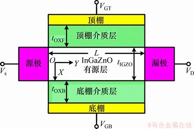
ͼ1���첽�Գ�˫դInGaZnO TFT������ṹ
Fig. 1��Cross sectional view of independent symmetric double-gate InGaZnO TFTs
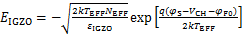
ͼ2��ʾΪInGaZnO TFT��Դ���̬�ܶ�ģ��[20]������InGaZnO TFT���ڵ�����(CBM)�ͼ۴���(VBM)����������������β̬�ܶ�gTA(E)������������̬�ܶ�gDA(E)����ʩ����β̬�ܶ�gTD(E)����ʩ������̬�ܶ�gDD(E)�����У�����InGaZnO�ṹ�ڲ�����ȱ�ݣ������γɴ�β̬�ܶ�gTA(E)��gTD(E)����InGaZnO������λ�ͷ������Ӻ��γ����Ҽ��������ڽ������γ�����̬gDA��gDD(E)[21]����Щ�ܼ��ı���ʽ���£�
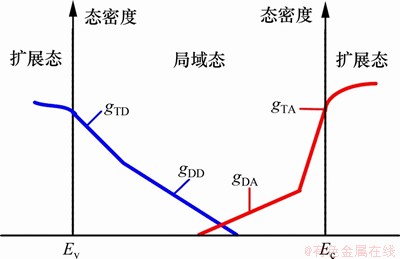
ͼ2��a-InGaZnO TFTs̬�ܶ�ʾ��ͼ
Fig. 2��Diagram of subgap density of state in InGaZnO active layer


���У�nTA��nDA��nTD��nDD�ֱ�ΪTA��DA��TD��DD��4��ȱ��̬�ܶȷֲ�������Ũ�ȣ�kΪ��������������TTA��TDA��TTD��TD�ֱ�Ϊ��4��ȱ��̬�ܶȵ���Ч�����¶ȣ�EC��EV�ֱ�Ϊ������(CBM)�ͼ۴���(VBM)��������
���ǵ�InGaZnO��ĤΪ����/�����N�Ͱ뵼����ϣ�Ӱ�칵�����Ʒֲ��IJ��������������ӣ������о���̬�����ӣ�InGaZnO TFT�Ĺ�������Ӧ���㲴�ɷ��̣�
ʽ�У���Ϊ�����ܶ�(C/cm3)����IGZOΪ�Ǿ�InGaZnO�Ľ�糣����nfreeΪ�����������ܶȣ�

����ȱ��̬�ܸ��ӣ����²��ɷ����������ѣ�������Ч�������ܶ�


ʽ�У�NEFFΪ��Ч�������ܶȣ������ֵΪ5��1018 cm-3��eV-1[23]��kΪ��������������k=1.380 649��10-23 J/K��TEFFΪ��Ч�����¶ȣ�TEFF =300 K��kTEFFΪ��Ч����������kTEFF=0.026 eV��VCHΪy�����ϵĹ�����ѹ����F0Ϊ�����ܼ���
���õ�����ʽ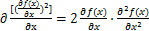

���ݸ�˹������InGaZnO��Ķ�դ���դ������Ӧ�÷ֱ��������±߽�������
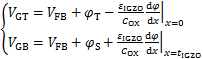
ʽ�У�COXΪ��λ���դ��������ݣ���T�ͦ�S�ֱ�Ϊ��դ�͵�դ�����ƣ�ͨ��ʽ(4)��ʽ(5)�����x=tIGZO���Ħ�S��


Ȼ����ʽ(6)���õ��ı����Ʀ�S�ǹ��ڵ�դ��ѹVGB�����������в���ֱ�����ڼ��㡣Ϊ����æ�S��VGB��ֱ�ӹ�ϵ��Ӧ����������ķ�ʽ��
Ӧ��Lambert W������=W(x)���Խ�ñ�����Ϊ
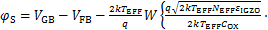

ʽ�У�W��ʾLambert W��������Ȼ��ʽ(8)�ɵñ�������ƫ�õ�ѹ�Ĺ�ϵ����Lambert W���ڳ�Խ������������Ƕ��SPICE����[24]�����б�Ҫ����TFT��ʵ�ʹ����������ʽ(8)�����ʵ��������������ڵ�ͨ��(VGB-VFB-��F0>VCH)ʱ��W���е�ָ�����ֿ�������ʱ���ɽ�Lambert W��������Ϊ


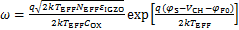
����������(VGB-VFB-��F0<>CH)ʱ��W�����Ϊ0�����ڦ�S�ܵ���դƫ�õ�ѹ��Ӱ�죬��ʱ����SΪ

ʽ�У��˱�����դƫ�õ�ѹVGT�Ա����Ʀ�S�ĵ���������ȡ����դ���������Դ��ĵ�Ч���ݵı�ֵ��VFB*Ϊ��Чƽ����ѹ����ȡֵ�붥դ��ƫ�õ�ѹ�йء���InGaZnO TFT�п���դ���������Դ�㲿�ֵ���Դ�����ΪCACT�����������ΪCOX�������ƻ����������ڵ�դ��ѹ��դ���ʲ����Դ���ϵķ�ѹ���˿ɱ�ʾΪ

һ��أ�ƽ����ѹ�ɷ�ΪVFB1��VFB2�����У�VFB1������������뵼�������ܴ�������Ӱ�죬��ȡ����դ��������ϡ��뵼���������Ũ�ȵȡ����磬��դ���������Ϊ��(Mo)ʱ��VFB1=-4.6 V[26]��VFB2���������㼰�����ɵ�Ӱ�졣�ڶ�դ��ѹVGT�ĵ����£�InGaZnO��������ӽ��ܵ�Ӱ�죬��Чƽ����ѹVFB���Ա�ʾΪ

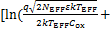
ʽ�У�a�ɾ����ȷ����Ϊ�˽�ʽ(9)��ʽ(10)ͳһ��1�������ı���ʽ����������tanh(x)��Ϊƽ������[27]���ɴ����յõ������Ʀ�S��������ʽ��


2 ����ģ�͵���֤
Ϊ����֤����ģ�͵���Ч�ԣ�ʹ��Silvaco TCADģ��ͼ1��ʾ��InGaZnO TFT�����Ƚ�����ģ�ͼ�������TCADģ���������У���դ��ѹ����դ��ѹ�����ƫ���������ṹ�Գƣ���VGT��VGB��tOXF=tOXB����1��ʾΪģ��ͼ��������InGaZnO TFT�����������������̬�ܶȡ�InGaZnO TFT��ƫ������Ϊ��©Դ��ѹVDS=0.1 V����դ��ѹVGT�ֱ�̶�Ϊ-4��-5��-6 V��������ʵ��Ӧ���У�����ö�����ѹƫ�ö�դ�Լ���TFT��й©�����������ص㿼����Ƶ�ѹVGTС��0 V�����������VGT����0 V��������ɲο�����[8��22]����դ��ѹVGB��0 Vɨ�赽15 V����դ��ѹɨ����Ϊ0.5 V��
���������դ��ѹ�ı仯��ϵ��ͼ3�����У�ͼ3(a)��ʾΪL=40 ��mʱ���첽�Գ�˫դInGaZnO TFT�ı����Ʀ�S���դ��ѹVGB�仯�ļ�������TCAD��ֵģ��������ͼ3(a)�ɼ�����VGB��Сʱ����S��VGB�������������VGB�ϴ�ʱ����S�ӽ��ڱ���ֵ����һ���棬��դ��ѹVGT���������ĵ��������Եĵ������ã���VGT����ʱ����S����������ڱ��ͣ��ڲ�ͬ�Ķ�դ����դ��ѹ�£���S����ֵ�����ֵ�Ǻϳ̶ȶ��ϸߡ�ͼ3(b)����ʽ(8)��ʽ(13)�ļ���ֵ���ϳ̶Ƚϸߣ���˵������Lambert W�����Ľ��ƽϺ������������ģ���нϸߵĿ��Ŷȡ�
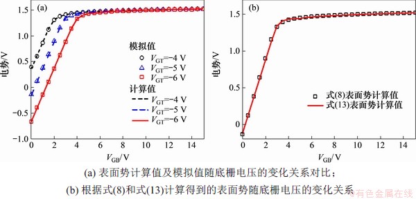
ͼ3�����������դ��ѹ�ı仯��ϵ
Fig. 3��Relationship between surface potential and bottom-gate voltage
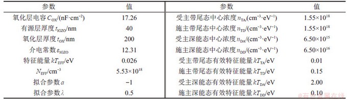
��1��InGaZnO TFTģ��ģ��ͼ���IJ���ȡֵ
Table 1��InGaZnO TFT parameters for TCAD simulation and model calculation.
3 ���������
��TCAD�ķ������У�����դ��ѹVGTΪ-5 V����դ��ѹVGBΪ15 Vʱ���첽˫դInGaZnO TFT����������Ũ�Ⱥ������Ʒֲ���ͼ4����ͼ4(a)�ɼ���InGaZnO TFT�ĵײ�����������������Ũ�����ԼΪ1018 cm-3�������������й��ɵ���СΪ1011 cm-3����ͼ4(b)�ɼ���InGaZnO TFT�Ĺ����ײ�����ԼΪ15 V���ӵײ���������С��������Ϊ����դ��ѹVGBΪ15 Vʱ���������������ӻ����ڹ�����դ��Ե��֮��Ľ��洦���õ��ӻ��۲������˵�դ�糡�����ã������첽˫դInGaZnO TFT�����Ʀ�S���ŵ�դ��ѹVGB�����Ӷ����ڱ��ͣ���������ʽ(9)��ʾ��һ�¡���Դ�㶥���ı�����ƺ͵ײ������Ʊ仯����һ�£�ֻ������ֵ�����������������ڹ�����ɻ��۶Ե糡�����������ڹ����㶥���͵ײ����ڲ��졣
����ģ�ͱ���ʽ����õ��IJ�ͬ��Դ����tIGZO�Ͳ�ͬ��������tOX�������Ʀ�S���դ��ѹVGB�ı仯��ϵ��ͼ5����ͼ5�ɼ���������Դ����tIGZO��30 nm������50 nm����S������������VGB���Ӹ���ؽӽ�����ֵ��������������tOX��200 nm������220 nm�����Ʊ���ֵ��С����S�������������仯��������Ϊ��S�ı���ֵ�ɱ߽�ʽ(5)��������������Դ���ȵ�Ӱ�죻��tIGZO���ӻᵼ�¹�����������������Ŀ���ӣ����ԣ���S����VGB���Ӹ���شﵽ����ֵ����һ���棬tOX���ӵ��µ�λ�����դ���ʵ��ݼ��٣������ڹ�����դ��Ե��֮��Ľ��洦�������ӱ��٣���ѹҲ��Ӧ�ؼ��٣����ԣ��������Ħ���Ϊ1/2���������ĵ��Ʋ��䣬�������ĵ�����֮��С��
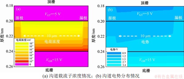
ͼ4�����������Ӽ����Ʒֲ�ͼ
Fig. 4��Channel electron concentration and channel potential distribution
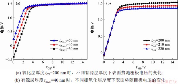
ͼ5����ͬ�IJ��ϲ����±�������դ����ѹ�ı仯
Fig. 5��Relationship between surface potential and gate voltage at different material thicknesses
InGaZnO TFT�ĵ�ѧ������InGaZnO��Ĥ��ȱ��̬�ܶȵ�Ӱ��ܴ�[28]��Ϊ�˽�һ���о�InGaZnO TFT�������ܵ�ʵ��ȱ��̬�ܶȵ�Ӱ�죬����TCAD����InGaZnO TFT��4��ȱ��̬�ܶȶԱ����Ƶ�Ӱ�죬ȱ��̬�ܶ�ȡֵ���1��ʾ���ڲ�ͬ��������β���ķֲ�Ũ��nTA���������������ķֲ�ŨnDA�£������Ʀ�S���դ��ѹVGB�仯�Ĺ�ϵ��ͼ6����ͼ6(a)�ɼ�����nTA��1.55��1016 cm-3��eV-1���ӵ�6.5��1020 cm-3��eV-1ʱ�������Ƶ�ͨ����nTA���Ӷ�����С����ͼ6(b)�ɼ�����nDA��6.5��1014 cm-3��eV-1���ӵ�6.5��1018 cm-3��eV-1ʱ�������Ƶ�ͨ����nDA���Ӷ�������С��������Ϊ��������̬�ɷ������������ӣ�nDA���ӵ��¹������Ӽ��٣��Ӷ��糡��С����ͨ�������Ƽ�С��
���ձ����������ĵ���ģ�ͣ���nDA��6.5��1014 cm-3��eV-1�仯��6.5��1018 cm-3��eV-1ʱ����Ӧ������ģ���е�NEFF��6.5��1016 cm-3��eV-1�仯��6.5��1020 cm-3��eV-1����ͼ6(b)�ɼ���TCAD����ģ��ֵ��ģ�ͼ���ֵ�����Ǻϣ���������10�����ڡ���ע����ǣ���Ч�������ܶȶ���Ϊ���������Ӵ�β̬������̬����Чֵ����InGaZnO TFT��ȱ��̬�ķ�ΧΪ1016~1022 cm-3��eV-1[29]������NEFF�ľ���ֵԼΪnDA��100����
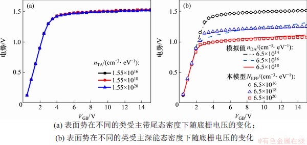
ͼ6���������ڲ�ͬ��������̬�ܶ������դ��ѹ�ı仯
Fig. 6��Relationship between surface potential and gate voltage at different acceptor-like states

ͼ7���������ڲ�ͬ����ʩ����̬�ܶ������դ��ѹ�ı仯
Fig.7��Relationship between surface potential and gate voltage at different donor-like states
ͨ��TCAD�����õ���ͬ��ʩ����β���ķֲ�Ũ��nTD�Ͳ�ͬ��ʩ���������ķֲ�Ũ��nDD����TCAD�����õ������Ʀ�S���դ��ѹ�仯�Ĺ�ϵ��ͼ7����ͼ7(a)�ɼ�����nTD��1.55��016 cm-3��eV-1���ӵ�6.5��1022 cm-3��eV-1ʱ������������������nTD���Ӷ������ӡ���ͼ7(b)�ɼ�����nDD��4.5��1016 cm-3��eV-1���ӵ�7.5��1016 cm-3��eV-1ʱ������������������nDD���Ӷ��������ӡ�������Ϊ��ʩ������̬�ܶ����ӵ��¹����е����ɵ������ӣ��Ӷ�Ӱ�쵽�������ĵ��Ʒֲ���
��������������ʩ��ȱ��̬��������������ģ���еĵ�Чƽ����ѹVFB�йأ�nDD��5.5��1016 cm-3��eV-1�仯��5.5��1016 cm-3��eV-1��Ч������ģ���е�VFB��0.3 V�仯��-0.1 V����ͼ7(b)�ɼ�TCAD����ģ��ֵ��ģ�ͼ���ֵ���Ǻϣ�������������5�����ڡ�
4 ����
1) �о��˶�����ѹƫ�����첽�Գ�˫դInGaZnO TFT�ı�����ƹ��ɣ���ͨ���������ɷ��̵õ��첽˫դInGaZnO TFT������ƵĽ���ģ�͡����ǵ����������InGaZnO TFT��ȱ��̬�ܶȵĹ����������Чƽ����ѹ�ĸ��������������Ĺ��������������������Χ���ܶ�դ��ѹ���Ե��Ƶ�����ģ��ֻ��Ҫ2����ϲ�������������ƽ������tanh(x)��ϵ�ͨ�������Ƶõ����������첽�Գ�˫դInGaZnO TFT�ı����ƽ���ģ�͡�
2) ��Դ���Ⱥ��������ȶԱ����Ƶ�Ӱ����Ҫȡ���ڹ����ͽ��洦��������Ũ�ȡ��������ı������������ȱ��̬�ܶ�����������������ı��������ʩ��ȱ��̬�ܶ��������С���ڲ�ͬȱ��̬�ܶ��£�����ģ�͵ĵ��Ƽ���ֵ��TCAD����ֵ�������С��10%��
�ο����ף�
[1] ZHAO Jiaqing, YU Pengfei, QIU Shi, et al. Universal compact model for thin-film transistors and circuit simulation for low-cost flexible large area electronics[J]. IEEE Transactions on Electron Devices, 2017, 64(5): 2030-2037.
[2] LI Yunpeng, YANG Jin, WANG Yiming, et al. Complementary integrated circuits based on p-type SnO and n-type IGZO thin-film transistors[J]. IEEE Electron Device Letters, 2018, 39(2): 208-211.
[3] FENG Guangdi, ZHAO Yuhang, JIANG Jie. Lightweight flexible indium-free oxide TFTs with AND logic function employing chitosan biopolymer as self-supporting layer[J]. Solid-State Electronics, 2019, 153: 16-22.
[4] HU Wennan, JIANG Jie, XIE Dingdong, et al. Transient security transistors self-supported on biodegradable natural-polymer membranes for brain-inspired neuromorphic applications[J]. Nanoscale, 2018, 10(31): 14893-14901.
[5] YU Fei, MA Xiaoyu, DENG Wanling, et al. A surface-potential-based drain current compact model for a-InGaZnO thin-film transistors in Non-Degenerate conduction regime[J]. Solid-State Electronics, 2017, 137: 38-43.
[6] CAI Minxi, YAO Ruohe. A threshold voltage definition for modeling asymmetric dual-gate amorphous InGaZnO thin-film transistors with parameter extraction technique[J]. Journal of Applied Physics, 2019, 125(8): 084503.
[7] ZONG Zhiwei, LI Ling, JIANG Jin, et al. A new surface potential-based compact model for a-IGZO TFTs in RFID applications[C]// 2014 IEEE International Electron Devices Meeting. San Francisco, CA, USA. IEEE, 2014: 35.5.1-35.5.4.
[8] QIN Ting, LIAO Congwei, HUANG Shengxiang, et al. Analytical drain current model for symmetric dual-gate amorphous indium gallium zinc oxide thin-film transistors[J]. Japanese Journal of Applied Physics, 2018, 57(1): 014301.
[9] ��С��, ������, ������, ��. InGaZnO��Ĥ�����й©����ģ��[J]. ����ѧ��, 2019, 68(5): 219-225.
DENG Xiaoqqing, DENG Lianwen, HE Yini, et al. Leakage current model of InGaZnO thin film transistor[J]. Acta Physica Sinica, 2019, 68(5): 219-225.
[10] JEONG H, KONG C S, CHANG S W, et al. Temperature sensor made of amorphous indium-gallium-zinc oxide TFTs[J]. IEEE Electron Device Letters, 2013, 34(12): 1569-1571.
[11] RIZZOLO S, GOIFFON V, ESTRIBEAU M, et al. Influence of pixel design on charge transfer performances in CMOS image sensors[J]. IEEE Transactions on Electron Devices, 2018, 65(3): 1048-1055.
[12] CAPOCCIA R, BOUKHAYMA A, JAZAERI F, et al. Compact modeling of charge transfer in pinned photodiodes for CMOS image sensors[J]. IEEE Transactions on Electron Devices, 2019, 66(1): 160-168.
[13] BIN WAN ZAIDI W M H , COSTA J, POURYAZDAN A, et al. Flexible IGZO TFT SPICE model and design of active strain-compensation circuits for bendable active matrix arrays[J]. IEEE Electron Device Letters, 2018, 39(9): 1314-1317.
[14] WANG Cuicui, HU Zhijin, HE Xin, et al. One gate diode-connected dual-gate a-IGZO TFT driven pixel circuit for active matrix organic light-emitting diode displays[J]. IEEE Transactions on Electron Devices, 2016, 63(9): 3800-3803.
[15] JEON C H, UM J G, MATIVENGA M, et al. Fast threshold voltage compensation AMOLED pixel circuit using secondary gate effect of dual gate a-IGZO TFTs[J]. IEEE Electron Device Letters, 2016, 37(11): 1450-1453.
[16] BILLAH M M, HAN J U, HASAN M M, et al. Reduced mechanical strain in bendable a-IGZO TFTs under dual-gate driving[J]. IEEE Electron Device Letters, 2018, 39(6): 835-838.
[17] TAUR Y. An analytical solution to a double-gate MOSFET with undoped body[J]. IEEE Electron Device Letters, 2000, 21(5): 245-247.
[18] SAHOO A, THAKUR P K, MAHAPATRA S. A computationally efficient generalized Poisson solution for independent double-gate transistors[J]. IEEE Transactions on Electron Devices, 2010, 57(3): 632-636.
[19] HUANG Junkai, DENG Wanling, ZHENG Xueren, et al. A compact model for undoped symmetric double-gate polysilicon thin-film transistors[J]. IEEE Transactions on Electron Devices, 2010, 57(10): 2607-2615.
[20] KAMIYA T, NOMURA K, HOSONO H. Origins of high mobility and low operation voltage of amorphous oxide TFTs: electronic structure, electron transport, defects and doping[J]. Journal of Display Technology, 2009, 5(7): 273-288.
[21] KAMIYA T, NOMURA K, HIRANO M, et al. Electronic structure of oxygen deficient amorphous oxide semiconductor a-InGaZnO4-x: Optical analyses and first-principle calculations[J]. Physica Status solidi(C), 2008, 5(9): 3098-3100.
[22] ����, ������, �δ�ά, ��. ͬ���Գ�˫դInGaZnO��Ĥ����ܵ���ģ���о�[J]. ����ѧ��, 2017, 66(9): 097101.
QIN Ting, HUANG Shengxiang, LIAO Congwei, et al. Analytical channel potential model of amorphous InGaZnO thin-film transistors with synchronized symmetric dual-gate[J]. Acta Physica Sinica, 2017, 66(9): 097101.
[23] FUNG T C, CHUANG C S, CHEN C, et al. Two-dimensional numerical simulation of radio frequency sputter amorphous In-Ga-Zn-O thin-film transistors[J]. Journal of Applied Physics, 2009, 106(8): 084511.
[24] ALVARADO J, INIGUEZ B, ESTRADA M, et al. Implementation of the symmetric doped double-gate MOSFET model in Verilog-A for circuit simulation[J]. International Journal of Numerical Modelling: Electronic Networks, Devices and Fields, 2010, 23(2): 88-106.
[25] HOORFAR A, HASSANI M. Inequalities on the Lambert W function and hyperpower function[J]. Journal of Inequalities in Pure & Applied Mathematics, 2008, 9(2): 1-5.
[26] MIGLIORATO P, SEOK M, JANG J. Determination of flat band voltage in thin film transistors: the case of amorphous-indium gallium zinc oxide[J]. Applied Physics Letters, 2012, 100(7): 073506.
[27] LI Can, LIAO Congwei, YU Tianbao, et al. Concise modeling of amorphous dual-gate In-Ga-Zn-O thin-film transistors for integrated circuit designs[J]. Chinese Physics Letters, 2018, 35(2): 27302.
[28] CHEN C, ABE K, KUMOMI H, et al. Density of states of a-InGaZnO from temperature-dependent field-effect studies[J]. IEEE Transactions on Electron Devices, 2009, 56(6):1177-1183.
[29] KIM Y, BAE M, KIM W, et al. Amorphous InGaZnO Thin-film transistors-part I: complete extraction of density of states over the full subband-gap energy range[J]. IEEE Transactions on Electron Devices, 2012, 59(10): 2689-2698.
(�༭ �²ӻ�)
�ո����ڣ� 2019 -12 -26; �����ڣ� 2020 -03 -10
������Ŀ(Foundation item)�������ص��з��ƻ���Ŀ(2017YFA0204600)�����ϴ�ѧ�����У��������ҵ��������Ŀ(2019zzts424) (Project(2017YFA0204600) supported by the National Key Research and Development Program of China; Project(2019zzts424) supported by the Fundamental Research Funds for the Central Universities of Central South University)
ͨ�����ߣ������ģ���ʿ�����ڣ�������Ϣ�����������������Ӽ������о���E-mail��denglw@csu.edu.cn
ժҪ������첽�Գ�˫դ�ṹ����������п(InGaZnO)��Ĥ�����(thin film transistors��TFTs)����Ⲵ�ɷ��̣�������������������������ͨ���IJ�ͬ�ֲ��ص㣬�������������Чƽ����ѹ�ĸ���ڵ�ͨ������Lambert W�������ƣ������첽�Գ�˫դInGaZnO TFT������ƽ���ģ�͡���ģ�͵���ϲ���ֻ��2�����ܹ��Ϻõط�ӳ�����ȡ�������ѹ�Ȳ����Ե��Ƶ�Ӱ�졣��������ģ�ͼ�TCAD�������о�InGaZnO���ȡ�դ���ʲ����Լ�ȱ��̬�ܶȵ��������Զ���դ��˫դ����ܱ�����Ƶ�Ӱ�졣�о������������������������������ŵ�դ��ѹ����ʽ��������������ڶ�դ��ѹ����������ƽ�ƣ��ڵ�ͨ��������������ŵ�դ��ѹ���������ͣ��ҵ���ֵ�붥դ���Ƶ�ѹ������ض�С��������ƵĽ���ģ����TCAD��ֵ�������Աȣ����нϸߵ��Ǻ϶ȣ��ڲ�ͬȱ��̬�ܶȷֲ�����£�����ģ�͵ļ���ֵ��TCAD����ֵ�������С��10%�����о��ɹ��������˽�˫դInGaZnO TFT�ĵ�ͨ���ƣ�������InGaZnO TFT��������ģ����ؼ��ɵ�·��ơ�
