

Microwave-assisted synthesis and characterization of ZnO-nanorod arrays
ZHU Jian-yu(�콨ԣ)1, 2, 3 , ZHANG Jing-xia(�ž�ϼ)2, ZHOU Hui-fen(�ܻ۷�)2,
QIN Wen-qing(������)2, 3, CHAI Li-yuan(����Ԫ)1, HU Yue-hua(������)2, 3
1. School of Metallurgical Science and Engineering, Central South University, Changsha 410083, China;
2. School of Minerals Processing and Bioengineering, Central South University, Changsha 410083, China;
3. Key Laboratory of Biometallurgy of Ministry of Education, Central South University, Changsha 410083, China
Received 10 August 2009; accepted 15 September 2009
Abstract:
High density ZnO-nanorod arrays (rod length 1.59 ��m) were successfully synthesized via a microwave-assisted solution-phase method using zinc chloride and ammonia solution as reactants. The influence of concentration of ammonia solution, work power, and microwave irradiation time on the morphology and size of final products was carefully investigated. The crystal structure, chemical composition and morphologies of final products were characterized using X-ray powder diffraction (XRD), scanning electron microscopy (SEM) and photoluminescence (PL). The as-synthesized ZnO is composed of single crystalline and possesses three photoluminescence emissions centered at 400, 469 and 534.5 nm, respectively.
Key words:
ZnO-nanorod arrays; microwave-assisted synthesis; photoluminescence;
1 Introduction
Zinc oxide (ZnO) is one of the most important ��-�� semiconductors with a wide band gap (3.37 eV) and large binding energy at room temperature, which has attracted much attention due to its unique properties. ZnO nanocrystal has found numerous applications, such as gas sensors[1], transparent electrodes[2], pH sensors [3], biosensors[4], acoustic wave devices[5], and UV photodiodes[6]. The morphologies and sizes of inorganic materials are well-known to determine their physicochemical properties. Nowadays, there has been an increasing interest in the fabrication of ZnO with uniform size and various morphologies, including low-dimensional ZnO nanostructures such as nanowires [7], nanorods[8], nanotubes[9-10], and nanosheets[11]; and self-assembled ZnO with low-dimensional structure- based morphologies, such as nanocombs[12], nanobridges [13], nanoflowers[14], nanodendrons[15], nanowaxberry [4], and nanobilayer[16], has also been synthesized by different approaches such as thermal evaporation method[13], microwave heating[17], non-aqueous approaches[18], chemical vapor deposition (CVD)[19], sol-gel process[20], gas condensation[21], hydrothermal process[22], laser ablation[23], template-assisted growth [24], and refluxing method[25].
As an environmentally benign technology with wide applications, microwave synthesis has the advantages of homogeneous volumetric heating, and high reaction rate compared with other physical and chemical methods. Herein, we report the synthesis and characterization of ZnO-nanorod arrays through the microwave method without any catalysts, templates, and substrates using zinc chloride as zinc source, and strong aqua ammonia as both alkaline and complexing reactant. The crystallinity, structure and morphology of ZnO nanocrystals are characterized. Furthermore, the room temperature photoluminescence (PL) is also examined. In particular, the effects of the concentration of aqua ammonia, work power, and microwave irradiation time on the morphology of ZnO nanostructures are investigated.
2 Experimental
All chemicals were of analytical grade from Shanghai Chemical Reagents Co., China, and were used as starting materials without further purification.
2.1 Synthesis of ZnO-nanorod array
In a typical procedure, zinc chloride was added into a glass beaker of 100 mL capacity with 40 or 80 mL deionized water. The zinc chloride(1 or 2 mmol) was dissolved assisted with ultrasound equipment. Then ammonia solution (28%) was added dropwise to the above solution with constant stirring. After stirring at room temperature for 5 min, the above samples were irradiated by microwave energy using the microwave oven (Midea, KD23B-DA, 2.45 GHz, maximum power 800 W). After microwave processing, the solution of the mixture was cooled to room temperature naturally. The resulting precipitates were collected by filtration and washed with deionized water for several minutes. The final products were dried in a vacuum box at 60 �� for 2 h. The usage of reactants, irradiation time and work power of the microwave oven in different reactions are described in Table 1. Sample 5 and 7 are prepared with 2.0 mmol ZnCl2, 10.0 mL NH3 ��H2O, and 80 mL H2O.
Table 1 Synthesis parameters of ZnO samples produced in different reactions
2.2 Characterization
The obtained samples were characterized on a Brucker D8-advance X-ray powder diffractometer (XRD) with CuK�� radiation (��=1.541 8 ?). The operation voltage and current were kept at 40 kV and 40 mA, respectively. The size and morphology of the as-synthesized products were determined at 20 kV by a XL30 S-FEG scanning electron microscope (SEM). The room temperature photoluminescence measurement was carried out on an F-2500 spectrophotometer using the 320 nm excitation line of Xe light.
3 Result and discussion
The XRD pattern of the as-prepared ZnO-nanorod arrays using 1.0 mmol ZnCl2 and 5.0 mL NH3 ��H2O solution at the power of 30% for 20 min is shown in Fig.1. All diffraction peaks can be indexed to hexagonal ZnO with lattice constants a=3.249 ? and c=5.208 ?, consistent well with the standard PDF database (JCPDS file 36-1451). The characteristic peaks are higher in intensity and narrower in spectral width, indicating that the products are of good crystallinity. No peaks corresponding to impurities are detected, showing that the final products purely consist of ZnO.
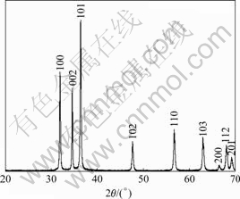
Fig.1 XRD pattern of as-prepared ZnO-nanorod arrays using 1.0 mmol zinc chloride and 5.0 mL ammonia solution at power of 30% for 20 min
Fig.2 shows the typical SEM images of the products prepared using 1.0 mmol ZnCl2 and 5.0 mL NH3��H2O solution at power of 30% for 20 min. The image clearly reveals that the bulk-shaped structures are composed of nanorods. The detailed geometrical morphology was checked using high-magnification SEM and the corresponding image is shown in Fig.2(b). From Fig.2(b) the ZnO-nanorod arrays assembled from ZnO-nanorods can be clearly observed. The nanorods lined up with each other are about 1.1 ��m in length and 0.63 ��m in diameter, though a few flowers can be found. The EDS spectrum of ZnO is shown in Fig.3. The results show the presence of Zn and O (C signal comes from C substrate), which agrees well with the XRD pattern.

Fig.2 (a) SEM image of as-prepared ZnO-nanorod arrays using 1.0 mmol zinc chloride and 5.0 mL ammonia solution at power of 30% for 20 min; (b) SEM image of same sample at higher magnification

Fig.3 EDS pattern of ZnO-nanorod arrays prepared using 1.0 mmol zinc chloride and 5.0 mL ammonia solution at power of 30% for 20 min
The concentration of NH3��H2O, work power, and microwave irradiation time have influences on the size and morphology of ZnO microstructures. Fig.4(a) shows the typical SEM image of products prepared with 3.5 mL NH3��H2O, which shows underdeveloped flower-like ZnO microstructures. Raised buds and quasi-triangular petals which are about 0.88 ��m in length can be seen clearly. When the volume of NH3��H2O is 7.5 mL, the products transform into cluster-like arrays; the petals have been enlarged; and the number of them decreases, as shown in Fig.4(b). The morphological evolution of ZnO nanostructures suggests that the growth of ZnO is susceptive to the added volume of ammonia solution in this system, and proper amount of ammonia solution is crucial for the formation of ZnO nanorods while keeping the self- assembly structures of final products.
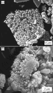
Fig.4 SEM images of ZnO prepared using 1.0 mmol zinc chloride with different concentrations of ammonia at power of 30% for 20 min: (a) 3.5 mL ammonia solution; (b) 7.5 mL ammonia solution
The morphology and size of ZnO nanostructures are very sensitive to the work power. Fig.5 presents the morphology of samples prepared under the power of 10% and 50%, respectively. The two samples(sample 4 and 5) show somewhat irregular morphology, indicating increasing or decreasing the work power also does not favor the formation of ZnO microstructures.
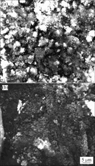
Fig.5 SEM images of ZnO nanostructures obtained at various conditions: (a) 1.0 mmol zinc chloride and 5.0 mL ammonia solution at power of 10% for 20 min; (b) 2.0 mmol zinc chloride and 10.0 mL ammonia solution at power of 50% for 20 min
The shape and size of ZnO nanostructures are also affected by microwave irradiation time in the synthesis process. Fig.6(a) shows the typical SEM image of products obtained at the power of 30% for 10 min. The products reveal irregular morphology, indicating short irradiation time does not favor the formation of ZnO microstructures. When the irradiation time is prolonged to 40 min, the products show the presence of flower-like ZnO. The flower morphology consists of sharp nanorods which look like petals with diameter of 1.5 ��m and the length of building units nanorods is also increased to 3.1 ��m as shown in Fig.6(b). Compared with the products shown in Fig.2(b), microstructures of Fig.6(b) change from nanorod array to flower-like. The results show that microwave irradiation time has great influence on the size and morphology of ZnO microstructures.

Fig.6 SEM images of ZnO nanostructures obtained at various conditions: (a) 1.0 mmol zinc chloride and 5.0 mL ammonia solution at power of 30% for 10 min; (b) 2.0 mmol zinc chloride and 10.0 mL ammonia solution at power of 30% for 40 min
The photoluminescence(PL) spectrum of the as-synthesized sample were investigated at room temperature under the excited wavelength of 320 nm. Fig.7 shows the PL spectrum of the sample prepared with 1.0 mmol ZnCl2 and 5.0 mL NH3��H2O. In Fig.7 three peaks can be found: UV band-edge emission centered at 400 nm, broad blue bands centered at 469 nm, and green bands centered at 534.5 nm. The PL signal at 400 nm is a typical ZnO near-band-edge (NBE) ultraviolet (UV) emission, which indicates a direct recombination of excitons through an exciton-exciton collision process[25]. Compared with ZnO nanorods that has a short wavelength region with a sharp band (378 nm) located at ultraviolet region by a microemulsion method[26], the microwave- assistedly synthesized ZnO exhibits a red-shift which may be ascribed to size effect, their unique morphology, and the heat-treatment condition[27-28]. The luminescence blue bands at 469 nm are caused by the transition from the level of the ionized oxygen vacancies to the valence band. The green transition at 534.5 nm referred to a deep-level emission is usually attributed to the presence of the ionized oxygen vacancy on the surface and results from the recombination of a photogenerated hole with a single ionized charged state of the defect in ZnO. Microwave- assistedly synthesized ZnO-nanorod arrays are formed in the atmosphere of deficient oxygen, which have caused large amounts of oxygen vacancies, so the peak of blue-green emission bands is very high.
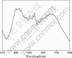
Fig.7 Room-temperature photoluminescence spectrum of ZnO-nanorod arrays prepared using 1.0 mmol zinc chloride and 5.0 mL ammonia solution at power of 30% for 20 min
4 Conclusions
1) High density ZnO-nanorod arrays were synthesized via a microwave-assisted solution-phase method using zinc chloride and ammonia solution as reactants without the need of a post-synthesis treatment. And then the products were characterized by XRD, SEM, and PL.
2) The nanostructures are influenced by microwave irradiation time, work power, and concentration of ammonia solution. Too high or too low work power will destroy crystal structure; the concentration of ammonia solution is crucial for morphology of ZnO nanorods; and irradiation time is also the key factor for the formation of ZnO nanostructures.
3) The room temperature photoluminescence spectrum of ZnO-nanorod arrays shows a blue emission at 469 nm and a broad visible emission in green region centered at 534.5 nm, and their UV-vis absorption peak shows a slight red-shift compared with ZnO nanorods (378 nm) by a microemulsion method, which may be referred to size effect, their unique morphology, and the heat-treatment condition.
References
[1] RAO B B. Zinc oxide ceramic semi-conductor gas sensor for ethanol vapour [J]. Materials Chemistry and Physics, 2000, 64(1): 62-65.
[2] HORSTHUIS W H G. ZnO processing for integrated optic sensors [J]. Thin Solid Films, 1986, 137(2): 185-192.
[3] ASIF M H, NUR O, WILLANDER M, DANIELSSON B. Selective calcium ion detection with functionalized ZnO nanorods-extended gate MOSFET [J]. Biosensors and Bioelectronics, 2009, 24(11): 3379-3382.
[4] CAO X, NING W, LI L D, GUO L. Synthesis and characterization of waxberry-like microstructures ZnO for biosensors [J]. Sensors and Actuators B: Chemical, 2008, 129(1): 268-273.
[5] KRISHNAMOORTHY S, ILIADIS A A. Development of high frequency ZnO/SiO2/Si Love mode surface acoustic wave devices [J]. Solid-State Electronics, 2006, 50(6): 1113-1118.
[6] LUO L, ZHANG Y F, MAO S S, LIN L W. Fabrication and characterization of ZnO film based UV photodetector [J]. Journal of Materials Science-Materials in Electronics, 2009, 20(3): 197-201.
[7] HUANG M H, WU Y Y, FEICK H, TRAN N, WEBER E, YANG P D. Catalytic growth of zinc oxide nanowires by vapor transport [J]. Advanced Materials, 2001, 13(2): 113-116.
[8] SUN X C, ZHANG H Z, XU J, ZHAO Q, WANG R M, YU D P. Shape controllable synthesis of ZnO nanorod arrays via vapor phase growth [J]. Solid State Communications, 2004, 129(12): 803-807.
[9] GENG B Y, LIU X W, WEI X W, WANG S W. Large-scale synthesis of single-crystalline ZnO nanotubes based on polymer-inducement [J]. Materials Research Bulletin, 2006, 41(10): 1979-1983.
[10] ZHANG X H, XIE S Y, JIANG Z Y, ZHANG X, TIAN Z Q, XIE Z X, HUANG R B, ZHENG L S. Rational design and fabrication of ZnO nanotubes from nanowire templates in a microwave plasma system [J]. Journal of Physical Chemistry B, 2003, 107(37): 10114-10118.
[11] BAI W, ZHU X, ZHU Z Q, CHU J H. Synthesis of zinc oxide nanosheet thin films and their improved field emission and photoluminescence properties by annealing processing [J]. Applied Surface Science, 2008, 254(20): 6483-6488.
[12] LAO J Y, WEN J G, REN Z F. Hierarchical ZnO nanostructures [J]. Nano Letters, 2002, 2(11): 1287-1291.
[13] LEE J S, ISLAM M S, KIM S. Photoresponses of ZnO nanobridge devices fabricated using a single-step thermal evaporation method [J]. Sensors and Actuators B-Chemical, 2007, 126(1): 73-77.
[14] SUH H W, KIM G Y, JUNG Y S, CHOI W K, BYUN D. Growth and properties of ZnO nanoblade and nanoflower prepared by ultrasonic pyrolysis [J]. Journal of Applied Physics, 2005, 97(4): 044305.
[15] GUPTA V, BHATTACHARYA P, YUZUK Y I, SREENIVAS K, KATIYAR R S. Optical phonon modes in ZnO nanorods on Si prepared by pulsed laser deposition [J]. Journal of Crystal Growth, 2006, 287(1): 39-43.
[16] CHEN J, LI C, SONG J L, SUN X W, LEI W, DENG W Q. Bilayer ZnO nanostructure fabricated by chemical bath and its application in quantum dot sensitized solar cell [J]. Applied Surface Science, 2009, 255(17): 7508-7511.
[17] KRISHNAKUMAR T, PINNA N, KUMARI K P, PERUMAL K, JAYAPRAKASH R. Microwave-assisted synthesis and characterization of tin oxide nanoparticles [J]. Materials Letters, 2008, 62(19): 3437-3440.
[18] CLAVEL G, WILLINGER M G, ZITOUN D, PINNA N. Solvent dependent shape and magnetic properties of doped ZnO nanostructures [J]. Advanced Functional Materials, 2007, 17(16): 3159-3169.
[19] ZANG C H, LIU Y C, ZHAO D X, ZHANG Y S. Growth and optical properties of ZnO microwells by chemical vapor deposition method [J]. Physica B: Condensed Matter, 2009, 404(2): 315-319.
[20] PETERSEN J, BRIMONT C, GALLART M, CREGUT O, SCHMERBER G, GILLIOT P, HONERLAGE B, ULHAQ-BOUILLET C, REHSPRINGER J L, LEUVREY C, COLIS S, SLAOUI A, DINIA A. Optical properties of ZnO thin films prepared by sol-gel process [J]. Microelectronics Journal, 2009, 40(2): 239-241.
[21] EILERS H, TISSUE B M. Synthesis of nanophase ZnO, Eu2O3 and ZrO2 by gas-phase condensation with cw-CO2 laser heating [J]. Materials Letters, 1995, 24: 261-265.
[22] PEI L Z, ZHAO H S, TAN W, YU H Y, CHEN Y W, ZHANG Q F. Single crystalline ZnO nanorods grown by a simple hydrothermal process [J]. Materials Characterization, 2009, 62(10): 3673-3675.
[23] SUN Y, FUGE G M, ASHFOLD M N R. Growth of aligned ZnO nanorod arrays by catalyst-free pulsed laser deposition methods [J]. Chemical Physics Letters, 2004, 396(1/3): 21-26.
[24] WANG Y F, ZHANG J H, CHEN X L, LI X, SUN Z Q, ZHANG K, WANG D Y, YANG B. Morphology-controlled fabrication of polygonal ZnO nanobowls templated from spherical polymeric nanowell arrays [J]. Journal of Colloid and Interface Science, 2008, 322(1): 327-332.
[25] YANG Y, WANG X H, SUN C K, LI L T. Photoluminescence of ZnO nanorod-TiO2 nanotube hybrid arrays produced by electrodeposition [J]. Journal of Applied Physics, 2009, 105(9): 094304.
[26] ZHANG R, YIN P G, WANG N, GUO L. Photoluminescence and Raman scattering of ZnO nanorods [J]. Solid State Sciences, 2009, 11(4): 865-869.
[27] XUE S W, ZU X T, ZHOU W L, DENG H, XIANG X, ZHANG L, DENG H. Effects of post-thermal annealing on the optical constants of ZnO thin film [J]. Journal of Alloys and Compounds, 2008, 448(1/2): 21-26.
[28] ZHANG J, SUN L D, YIN J L, SU H L, LIAO C S, YAN C H. Control of ZnO morphology via a simple solution route [J]. Chemistry of Materials, 2002, 14(10): 4172-4177.
Foundation item: Project supported by the Postdoctoral Science Foundation of Central South University, China; Projects(50621063, 30700008) supported by the National Natural Science Foundation of China
Corresponding author: ZHU Jian-yu; Tel: +86-13787242396, +86-731-88836944; E-mail: csuzhu@yahoo.com.cn
DOI: 10.1016/S1003-6326(09)60073-X
