
Interface structure of ultrasonic wedge bonding joints of Ni/Al
LI Jun-hui(�����), HAN Lei(�� ��), ZHONG Jue(�� ��)
(School of Mechanical-Electronical Engineering, Central South University, Changsha 410083, China)
Abstract:
Nickel plated on a copper plate was selected as a bond surface for ultrasonic aluminum wedge bonds, and a series of experiments were carried out to study the microstructure characterization of the wedge bond interface. Bond lift-off characteristics were studied by using scanning electron microscopy(SEM) with EDS-test. Characteristics of input power of PZT transducer were analyzed by the driving electric signal measured with GDS-820 Digital Oscilloscope. The results show that the pattern of partially bonded material at the Ni-Al interface of ultrasonic wedge bonds exposed by peeling underdeveloped bonds simulates a ridged torus with an unbonded central and external region rubbed along pulse direction. Bond strength is located between the severely ridged torus and the non-adhering central and external area of the bond. For the same machine variables, ridge-peak and transforming ultrasonic energy of the first wedge bond are greater than that of the second wedge bond. For constant other machine variables, with the increasing load, the total area of bond pattern increases in size, and minor axis of torus extends major axis; with the increasing time, the ridged periphery spreads a whole torus, and the ridged location of the bonded region moves closer to the bond center; the sliding trace and the ridge-like of the bond pattern strengthen when more power is applied. Moreover, the machine variables have an optimal range for microstructure characteristics.
Key words:
Ni/Al; electronics packaging; wedge bonding; microstructure; ultrasonic CLC number: TN45;
Document code: A
1 INTRODUCTION
Ultrasonic bonding was applied primarily to wire bonding in microelectronic packaging industry, while the mechanism of ultrasonic bonding wasn��t understood very well. One popular theory has suggested that interfacial rubbing causes a steep temperature rise, followed by a thermal deformation type of bond. The temperature rise at the welding surface was measured by the thermo-electromotive force between aluminum and copper specimens using a digital multimeter at a measuring speed of 2000 points/s by Tsujino et al[1], and the steep temperature rise was not caused. Harman[2, 3 ] and LI et al[4] determined that the interfacial temperature rise during bonding was not high (70-80��). The temperature rise at 25��m in diameter of Au-ball bonding surface was measured by using real-time temperature monitoring systems with 6��m in diameter of thermo-couples[5, 6], which was very low (20-25��). These temperatures were too low for the ultrasonic bond to be considered a thermally activated diffusion process. Intuitive friction weld idea was unreasonable.
The Young��s modulus of aluminum is reduced substantially when the acoustic energy is applied during a tensile testing[7, 8]. Such softening of metal under the influence of high-level acoustic radiation occurs in all of the materials studied (including aluminum, cadmium, beryllium, steel, zinc, copper, iron and gold)[9,10]. It is noticeable that ultrasonic energy softening effect for Al is 100 times as large as heating energy[11]. However, ��acoustic-plastic effect�� is elusive and the subject of much debate in physics. Some researchers thought that ultrasonic may increase atomic mobility and dislocation density of crystal lattice and remove brittle oxide on welding surface[12-16].
In this paper, characteristics at bonding micro-interface were observed by scanning electron microscopy and EDS-test, features of power of PZT transducer were analyzed by the driving electric signal measured with GDS-820 Digital Oscilloscope. Some phenomena and laws were researched firstly. They would be helpful for further research about ultrasonic bonding.
2 EXPERIMENTAL
The purpose of the experimental work was to investigate characteristics at bonding interface. So, nickel plated on a copper plate was selected as a bond surface for ultrasonic aluminum wedge bonds, and the major portion of this bonding program was performed using 500��m in diameter of aluminum wire and LW500 wedge capillary on U3000 ultrasonic wedge bonder at 60kHz.
First, bond lift-off microstructures at the first and the second bond were tested by SEM (KYKY2800) with EDS-test (Finder TM).
Second, to understand different characteristics of the first bond and the second bond, the power of PZT transducer was analyzed by the voltage and current signal of PZT transducer gotten by GDS-820 Digital Oscilloscope during the wedge bonding process.
Finally, as interface of the second bond was lifted up more easily than that of the first bond under the same machine variables, the second bond interface was selected to research relationship between microstructure and force, time and power, and a great deal of adjusting experiments on machine variables were carried out.
3 RESULTS AND DISCUSSION
3.1 General characteristics of bonds
Fig.1 shows the welding process of the first and the second wedge bonding.
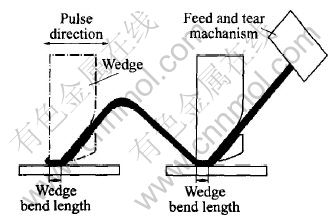
Fig.1 Comparison of first and second bond
Fig.2 shows that the pattern of partially bonded material at the Ni-Al interface of ultrasonic wedge bonds exposed by peeling underdeveloped bonds simulates a ridged torus with an unbonded central and external region rubbed along pulse direction.
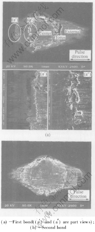
Fig.2 SEM images of bond lift-off patterns
Fig.2(a��) shows that ridged torus is physically destroyed and forms bonding strength. The region between torus and external is contracted. This is surface tension result in outer shrink during ultrasonic hardening process. Fig.2(a��) is similar to Fig.2(a��), and like small ridged torus, while Fig.2(a��) is much weaker than Fig.2(a��). It is the result of grads distribution in ultrasonic fields along wedge capillary. Ridged torus is the result of strong ultrasonic fields formed directly along wedge capillary, while weak ultrasonic fields generate indirectly along Al wire transmitting in small ridged torus.
Fig.3 shows EPMA scanning curve of cross-section at wedge bonding joints. It can be seen that Ni and Al atom diffuse each other during bonding process, and that diffusion depth is about 2��m.
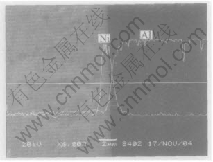
Fig.3 EPMA scanning curves of cross-section at bonding joints
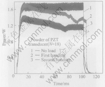
Fig.4 Power curves of PZT transducer in bonding process
The pattern of the first bond looks like shape of hollow fireball along pulse direction. Fig.1 shows that one end of the first bond is unrestrictive, another is restricted by hole of wedge capillary. So, torus at unrestricting end contracts closer to the bond center, and major axis decreases, otherwise another end looks like blaze along pulse direction. Moreover ridge of the first bond is much severer than that of the second bond.
The pattern of the second bond looks like egg section along pulse direction. Fig.1 shows that both ends of the second bond are restricted, thus microstructure features of the second bond appreciably differ from that of the first bond. And interface performance of the second bond decreases.
Microstructure difference of the first bond and the second bond shows that the bond strength of the first bond is greater than that of the second bond under the same machine variables. So, when Al wire is pulled up by using pull tester, interface of the second bond is lifted up firstly. To balance strength of the first bond and the second bond, machine variables of the second bond increase properly in wedge operation.
3.2 Power of PZT transducer
The power of PZT transducer is
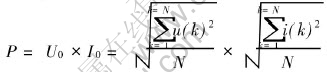
where U0 and I0 are the root mean square calculation; u(k) and i(k) are the sampling data in certain time, N is the sampling numbers, and N must be more than the data numbers of electric signal in a period. In this experiment, sampling frequency is 500kSa/s, the data number of electric signal in a period is 9.
So, RMS(root mean square) calculation was used to analyze the power of PZT transducer. The calculation results on no load, the first bond and the second bond are shown in Fig.4 by using Matlab, where N=18. Power of no load minus that of load (the first bonding or the second bonding) is transforming ultrasonic energy at interface. From the curves, it can be seen that transforming ultrasonic energy of PZT for the first bond is greater than that of the second bond. So, interface at the first bond is adhered better than that of the second bond. It is the reason why restrictions of the first bond are less than those of the second bond.
In summary, performances of the first bond are better than those of the second bond, and conclusions drawn by analyzing the power of PZT consist with the results gotten by testing microstructures at interface.
3.3 Microstructure evolutions
Microstructure evolutions include the changing of ridged area, rubbing regions, total area and so on. Characterizing variations are associated with the normal bond parameters-load, power and time.
3.3.1 Load effect
For constant time (350ms) and power (24W), experiments were carried out by adjusting load from 0.3N to 12.0N. Fig.5 shows that, for constant time and power, with the increasing load, the total area and torus of bond pattern increase in size, and minor axis of torus extends major axis along pulse direction.
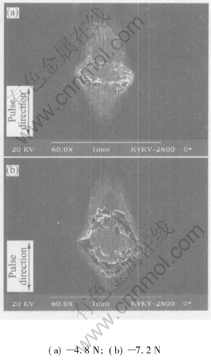
Fig.5 Patterns of increased force
Area curves including total bonding area, torus and center were calculated by using AutoCAD. Measuring area data are filled in graph (Fig.6). From area curves it can be seen that bonding area is proportional to load. When the load is 8.4N, an inflexion is indicated, and total area and torus reach saturating value basically.
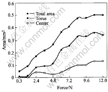
Fig.6 Relationship between area and force under 24W at 350ms
If load isn��t forced during bonding process, there is neither rubbing trace nor ridge-like at bonding interface. After ultrasonic softening effect, load must be forced for softened metal to be flowed, thus bonding regions are spread. The flow is limited when poor load is applied, and the characteristics at bonding interface decrease by using excessive loading.
3.3.2 Time effect
For constant power (24W) and load (9.6N), experiments were carried out by adjusting time from 10 ms to 500ms. Fig.7 indicates that for constant power and load, with the increasing time, the ridged periphery spreads a whole torus, and the ridged location of the bonded region moves closer to the bond center. Over-bond will be generated for excessive bonding time, and decrease such characteristics as crack and hardening of bond interface.
3.3.3 Power effect
For constant load (9.6N) and time (350ms), experiments were carried out by adjusting power from 3W to 30W. Fig.8 indicates that for constant load and time, the sliding trace and the ridge-like of the bond pattern strengthen when excessive bonding power was applied.
Ultrasonic energy is the product of power and time. For no ultrasonic energy, i.e. power or time is zero, no traces be generated at bonding interface.
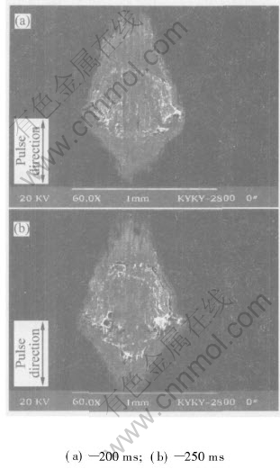
Fig.7 Patterns of increased time
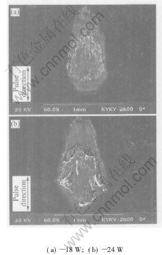
Fig.8 Patterns of increased power
4 CONCLUSIONS
1) The pattern of partially bonded material at the Ni-Al interface of ultrasonic wedge bonds exposed by peeling underdeveloped bonds simulates a ridged torus with an unbonded central and external region rubbed along pulse direction. Bond strength is located between the severely ridged torus and the non-adhering central and external area of the bond. For the same machine variables, ridge-peak, transforming ultrasonic energy of the first wedge bond are greater than those of the second wedge bond. Interface at the first bond is adhered better than that of the second bond. Some conclusions drawn by analyzing the power of PZT consist with results gotten by testing microstructures at the interface.
2) For other machine variables being constant, with the increasing load, the total area of bond pattern increases in size, and minor axis of torus extends major axis. With the increasing time, the ridged periphery spreads a whole torus, and the ridged location of the bonded region moves closer to the bond center, and the sliding trace and the ridge-like of the bond pattern strengthen when more power is applied.
REFERENCES
[1]Tsujino J, Yoshihara H, Kamimoto K, et al. Welding characteristics and temperature rise of high frequency and complex vibration ultrasonic wire bonding [J]. Ultrasonics, 2002, 36(2): 59-65.
[2]Harman G G. Wire Bonding in Microelectronics(2nd edition) [M]. New York: McGraw-Hill Publishing House, 1997. 18-23.
[3]Harman G G. Wire bonding to advanced copper, low-K integrated circuits, the metal/dielectric stacks, and materials considerations [J]. IEEE Trans Parts Hybrids Manuf Technol, 1990(13): 176-181.
[4]LI Jun-Hui, HAN Lei, ZHONG Jue. Microstructure characteristics at the thermosonic bond interface [J]. China Mechanical Engineering, 2005,16(4): 341-344.
[5]Suman S, Gaitan M, Joshi Y, et al. Wire bond temperature sensor [J]. Georgia Institute of Technology, 2002, 1(1): 1-6.
[6]Schwizer J, Mayer M, Bolliger D, et al. Thermosonic ball bonding: friction model based on integrated microsensor measurements [A]. The 25th IEEE/CPMT International Electronic Manufacturing Technology Symposium IEMT [C]. Austin,Texas, 1999. 108-114.
[7]Ivy W Q, Paul B, Dave D. Wedge bonding for ultra fine pitch applications [J]. Kulicke & Soffa, 2003, 2(1): A1-A10.
[8]Elenius P, Levine L. Comparing flip-chip and wire-bond interconnection technologies [J]. Chip Scale Reiew, 2000, 8: 81-87.
[9]Kang S Y, Williams P M, Mclaren T S, et al. Studies of thermosonic bonding for flip-chip assembly [J]. Materials Chemistry and Physics,1995, 42: 31-37.
[10]WANG Chang-hai, Holmes A S. Laser-assisted bumping for flip chip assembly [J]. IEEE Transaction on Electronics Packaging Manufacturing, 2001, 24(2): 109-114.
[11]TAN Qing, Schaible B, Leonard J, et al. Thermosonic flip chip with a self-planarization feature using polymer [J]. IEEE Transaction on Components, Hybrids, and Manufacturing Technology, 1998, 32(5): 1-8.
[12]Snitka V, Ulcinas A, Rackaitis M, et al. Ultrasonic surface vibration investigation by atomic force microscopy [J]. Ultrasonic, 1998, 36: 499-503.
[13]GAO Wei-lou, Tittmann B R, Miyasaka C. Contrast mechanism of ultrasonic atomic force microscopy [J]. IEEE Ultrasonics Symposium, 1999, 24(6): 601-604.
[14]Krzazowski J E. A transmission electron microscopy study of ultrasonic wire bonding [J]. IEEE Transaction on Components, Hybrids, and Manufacturing Technology, 1995, 13(1): 176-182.
[15]TAN Chen Ming, GAN Zheng-hao. Failure mechanisms of aluminum bond pad peeling during thermosonic bonding [J]. IEEE Transactions on Device and Materials Reliability, 2003, 3(2): 44-50.
[16]Quan Q, Giles J B. Mechanism of removal of micron-sized particles by high-frequency ultrasonic waves [J]. IEEE Transaction on Ultrasonics, Perroelectrics, and Frequency Control, 1995, 42(4): 619-629.
Foundation item: Project(50390064) supported by the National Natural Science Foundation of China; Project(2003CB716202) supported by the Major State Basic Research Development Program of China
Received date: 2004-09-18; Accepted date:2005-05-29
Correspondence: LI Jun-hui, PhD; Tel: +86-731-8836499; Fax: +86-731-8879044; E-mail: lijunhui@mail.csu.edu.cn
