
���±�ţ�1004-0609(2007)12-1916-06
Cr���Ӷ�Cu/Si(100)��Ĥ��ϵ���۽ṹ�������ʵ�Ӱ��
���½������δϣ��� ����������������ƽ
(�Ϻ���ͨ��ѧ ���Ͽ�ѧ�빤��ѧԺ ���������²��ϼ������ص�ʵ���ң��Ϻ� 200240)
ժ Ҫ��
���ü��Ͻ����Si(100)�ĵ״ſؽ����Ʊ�Cu��Cu-1.19%Cr��Cu-2.18%Cr��Ĥ���о�Cr��Cu��Ĥ��300~500 ������˻�ǰ��Ľṹ�͵����ʵ�Ӱ�졣X�����������������Cu��Cu(Cr)��Ĥ������Cu(111) ��Cu(200)����壬����Cu(Cr)��Ĥһֱ���ֽ�ǿ��(111)֯����ԭ����������������Cu��Ĥ��500 ���˻�ʱ����Ĥ�����������ԵĻ���ɢ����Ĥ��������ܶȼ�ƽ�����½�����Cu(Cr)��Ĥ���˻�ʱ���ֽϸߵ����ܶȣ�Cr�������Cu/Si��Ĥ��ϵ�����ȶ��ԡ�Cu(Cr)��Ĥ�ĵ��������¶������ȼ�С�������ӣ���400 �漰500 ���˻�30 min��ֱ�ﵽ��Сֵ2.76 �̦�?cm��2.97 �̦�?cm���봿CuĤ���(2.55 �̦�?cm)��Cu(Cr)��Ĥ�˻�����ʵĴ���ȼ�С�뱡Ĥ�����ߴ�������Լ�Cr����ɢ�йء�������Cr���Ӻͺ������˻���ʹ��Cu(Cr)�Ͻ�Ĥ�ڸ��»������Ϸ�����кܴ��Ӧ��ǰ����
�ؼ��ʣ�
Cu(Cr)��Ĥ��֯�������ȶ�������������
��ͼ����ţ�TM 241.1���� ���ױ�ʶ�룺A
Effect of chromium dopant on microstructure and resistivity characteristics of Cu/Si(100) systems
WANG Xin-jiang, LIU Jia-cong, HONG Bo, JIANG Chuan-hai, DONG Xian-ping
(Key Laboratory for High Temperature Materials and Testing of Ministry of Education,
School of Materials Science and Engineering, Shanghai Jiao Tong University, Shanghai 200240, China)
Abstract: Thin films of pure Cu and Cu with 1.19%Cr and 2.18%Cr were deposited by magnetron sputtering on Si(100) substrates. Samples were annealed at 300-500 �� in vacuum to investigate effects of Cr on the microstructure and resistivity characteristics of Cu/Si systems. X-ray diffraction reveals Cu(111) and Cu(200) peaks for Cu and Cu(Cr) films. However, Cu(Cr) films are textured in (111) orientation. Cr enhances the thermal stability of Cu/Si systems markedly. Resistivities of Cu(Cr) films after annealed at 400 �� and 500 �� are about 2.76 �̦�?cm and 2.97 �̦�?cm which approach to those of Cu films. The decrease of resistivity of annealed Cu(Cr) film can be attributed to the change of microstructure and microscopy of films and the diffusion of Cr. Once optimal amount of Cr and annealing procedures are determined, Cu(Cr) films can be applied as an electronic material resistant to high temperature.
Key words: Cu(Cr) films; texture; thermal stability; resistivity
�����������ɵ�·�IJ��Ϸ�չ�����нϵ͵ĵ����ʺߵĿ���Ǩ�����ܵ�ͭ��ȡ������Ϊ�����ģ���ɵ�·�����������ϡ���ͭ�����ߵ�����������µ����⣺����Cu��Si��SiO2 �ĵ��ǿ�Ȳ��߲��������о��к�ǿ����ɢ������[1-2]��Ŀǰ���õĽ���취���ڶ��߽���������赲�㡣���Ż����������ߴ�ļ�С(��100 nm�����赲���Ӧ�ò�����С��ͭ�Ŀ��ÿռ䣬�������ӳ�ЧӦ������Ӱ�����������ܡ�����ͭ��Ĥ�۽ṹ��Ӱ��������ͭ�Ͻ�Ĥ��Ӧ������������Խ��Խ���ע�⡣���������������ͨ��ͭ�ķǻ������γ�Ԫ�صĺϽ�������ͭ��Ĥ���ṹ�����ͭ�����ߵ�����[3-7]��Barmak��[4]��Kim��[8]��Cabral��[9]��ϸ�о���Cu-1%Cr(Ħ������)��Ĥ�ڲ�ͬ�˻�����е����ʵı仯�����Cu(Cr)�Ͻ�Ĥ���ھ��е͵��˻�����ʣ�����Ϊһ�ָ��»����߲��Ϸ�����кܴ��Ӧ��ǰ������Cu(Cr)��Ĥ�۽ṹ���о�һֱû�������㹻�����ӡ�
Ϊ�ˣ��������߲��õ��дſؽ��䷨�Ʊ�Cu(Cr)�Ͻ�Ĥ�������о�Cr��Cu/Si��Ĥ��ϵ�Ľṹ�Լ����ܵ�Ӱ�죬̽��Cu(Cr)�Ͻ�Ĥ������������Ӧ�õĿ����ԣ�Ϊ�������ϵĿ����ṩ�ο����ݡ�
1 ʵ��
����CEVP Gamma 1000c �Ͷ�дſؽ����Ǻ���ǶCrС��(99.9��)�ļ���ͭ(99.99��)�Ͻ�вģ�������Ƶ�ſؽ���ķ�ʽ��Si(100) �赥��Ƭ�������Ʊ��Ͻ�Ĥ[10]�������ǵı�����ն�Ϊ0.439~0.598 mPa����������Ϊ�����������ѹΪ0.665 Pa���ƾ�Ϊ27 cm�������¶�Ϊ���¡�
��ʵ���в���2�ֳɷֵİвģ�������ɷֱַ�ΪCu-2.06%Cr(Ħ����������ͬ)��Cu-4.04%Cr����Ƶ�ſؽ���Ľ��书��Ϊ100 W������ʱ��ֱ�Ϊ50 min��30 min��Ϊ���жԱȣ�ʵ�黹��ͬ���Ľ����������Ʊ��˴�ͭ��Ĥ������ʱ��Ϊ50 min��
��������ɢX����������(EDX)�Լ�Dektak 6M��̨���Dzⶨ2��ʱ���µĽ��䱡Ĥ�ɷֺͺ�ȷֱ�ΪCu-1.19%Cr(250 nm)��Cu-2.18%Cr(300 nm)�����ǵ���������ĵ��ʹ����¶�ԼΪ400 �棬��ʵ���г�����ı�Ĥ��300��400��500 ��������˻�30 min��
����X�������������(XRD)��Nanoscope ��a��ԭ��������(AFM)��SDY-5��˫�����̽������ǶԸ���Ĥ�Ľṹ�͵�����в��ԡ�����PHI550�Ͷ�Ъ����������(AES)���˻���Ԫ����ȷֲ����з�����AES��ȷ���ʱ�����ڽ����Ar����ǹ�����趨Ϊ3 keV��������ɨ�跶ΧΪ1 mm��1 mm�������������Ta2O5�궨��
2 ���������
2.1 ��Ĥ�۽ṹ�ı仯
ͼ1��ʾΪCu/Si��Cu(1.19%Cr)/Si��Cu(2.18% Cr)/Si��Ĥ��ϵ�˻�ǰ���XRD�ס���ͼ�п��Կ���������Ĥ������ͭ������壬����Cu(111)��Cu(200) ��Ϊ��������̬Cu��Ĥ��I(111)/I(200)ԼΪ2.5����ʱ��Ĥ���־�̬[11]������̬Cu(1.19%Cr)�� Cu(2.18%Cr)��Ĥ��I(111)/I(200)�ֱ�Ϊ4.69��3.91��Cu(Cr)��Ĥ���ֵ��͵�(111)֯���������˻��¶ȵ����ߣ�Cu(111)����ǿ��I(111)/I(200)ǿ�ȱ����ӡ�Cr�ļ���������ϵͳ�Ľ����ܣ���ʹ��(111)֯���ķ�չ[10, 12]��
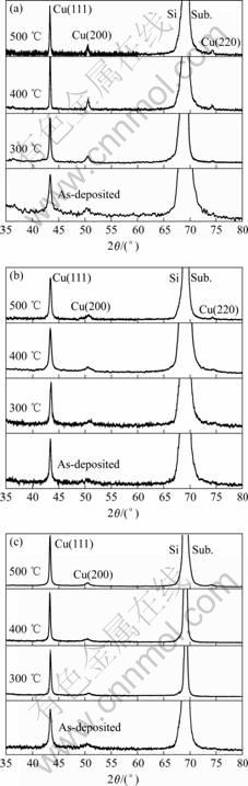
ͼ1 �˻�ǰ��Ĥ��ϵ��XRD��
Fig.1 XRD patterns of films at various annealing temperatures:
(a) Cu/Si; (b) Cu(1.19%Cr)/Si; (c) Cu(2.18%Cr)/Si
��ͭ��Ĥ��ȣ�����̬Cu(Cr)��Ĥ��Cu(200)�����Լ�С���˻�ʱCu(200)������ǿ��������Ϊ�����˻��¶ȵ����ߣ�Cu��Crԭ�ӵ���ɢ������ı�Ĥ��Ӧ���ܵ����ӵ�����Cu(200)�����ǿ��������300 ��ʱCr��Cu�е�����ɢϵ��Ϊ4.31��10-22 cm2/s[13]�����CuĤ��Cr�ij�����ɢֻ��ͨ�������뾧����С�����Cu(2.18%Cr) ��Ĥ���˻�ʱ�����Crƫ���ھ����ȱ�ݴ��������Cu��Crԭ����ɢ�ļ����ܣ���ʹ��ǿ��Cu(200)���γɵ��¶����ߡ�
2.2 ������ò
ͼ2~4��ʾ�ֱ�ΪCu/Si��Cu(1.19%Cr)/Si��Cu(2.18%Cr)/Si��Ĥ��ϵ��300��400��500 ���˻���AFM��Ƭ��Cu��Ĥ��300 ���˻�����������ӳߴ����ֲڶ��ɽ���̬��5.828 nm���ӵ�13.539 nm(ͼ2(a))��Cu(Cr)��Ĥ�˻��ı�����̬�뽦��̬��Ĥ�仯������ֲڶȷֱ���ԭ����2.140 nm��4.375 nm���ӵ�4.894 nm��7.375 nm[8]�����˻��¶ȼ������ߵ�400 ���500 ��ʱ����Cu��Ĥ��AFM��ò���Ա仯������ֲڶ����ӣ���Ĥ��֯�ṹ���ɣ����ܶ��½�������Cu��Ĥ�����䷢�������ԵĻ���ɢ����ʹ��Ĥ����ߵ������ƽ��Cu(Cr)�Ͻ�Ĥ���˻�������òû�з��������ı仯�����ܶȽϸߣ���Ĥ���ȶ���������ߡ�Cr������������ǿ��Cu/Si��Ĥ��ϵ�����ȶ��ԣ���С��Cu����е���ɢ��
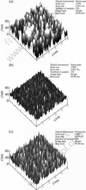
ͼ2 300 ���˻�30 min��Ĥ��ϵ��AFM��Ƭ
Fig.2 AFM images of annealed film systems at 300 �� for 30 min: (a) Cu/Si; (b) Cu(1.19%Cr)/Si; (c) Cu(2.18%Cr)/Si
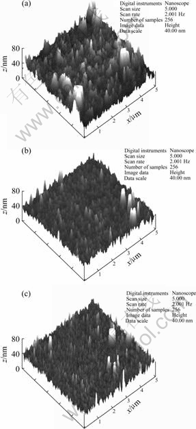
ͼ3 400 ���˻�30 min��Ĥ��ϵ��AFM��Ƭ
Fig.3 AFM images of annealed film systems at 400 �� for 30 min: (a) Cu/Si; (b) Cu(1.19%Cr)/Si; (c) Cu(2.18%Cr)/Si
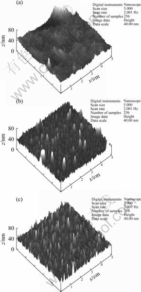
ͼ4 500 ���˻�30 min��Ĥ��ϵ��AFM��Ƭ
Fig.4 AFM images of annealed film systems at 500 �� for 30 min: (a) Cu/Si; (b) Cu(1.19%Cr)/Si; (c) Cu(2.18%Cr)/Si
2.3 ������ɢ
ͼ5��ʾΪCu/Si��Cu(1.19%Cr)/Si��Cu(2.18% Cr)/Si��Ĥ��ϵ400 ���˻���Ԫ��Ũ�ȷֲ����ߡ�Cu(Cr)��Ĥ��400 ���˻�ʱ������ϵͳ�����ܵ��Է���С(�����ߴ������)�Լ����������������ã��ֵ�Cr�ɱ�Ĥ�ڲ�������ɢǨ�������档�˻��Ĥ�����������ߴ�13����˵�����Cr�Ѿ���������Cr�Լ�Cr���������ڱ�Ĥ����ƫ�ۣ�ǿ���谭Cuԭ�ӵı�����ɢ�����������˸����±�Ĥ����Cuԭ�ӵ��žۣ����Cu/Si��Ĥ��ϵ�����ȶ��ԣ�ͬʱ������Cu(Cr)��Ĥ�ĵ����ʡ�����Cu(2.18%Cr)/ Si��Ĥ��ϵ�����ֵ�Cr�ڱ�Ĥ/�����洦ƫ�ۣ���Cu�������е���ɢ��һ�����赲���á�
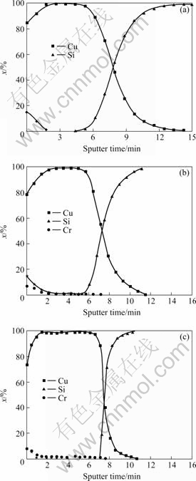
ͼ5 400 ���˻�30 min��Ĥ��ϵ��AESŨ����ȷֲ�
Fig.5 AES depth profiles of systems annealed at 400 �� for 30 min: (a) Cu/Si; (b) Cu(1.19%Cr)/Si; (c) Cu(2.18%Cr)/Si
2.4 �����ʵı仯
ͼ6��ʾΪCu/Si��Cu(1.19%Cr)/Si��Cu(2.18%Cr)/ Si��Ĥ��ϵ�ĵ��������˻��¶ȵı仯���ߡ�����̬Cu��Ĥ������Ϊ6.51 �̦�?cm��Զ���ھ�̬ͭ��Ĥ������(2 �̦�?cm)������Ͻ�Ԫ��Cr����̬��Ĥ�������������ӣ��ֱ�ﵽ13.07 �̦�?cm(Cu(1.19%Cr))��20.43 �̦�?cm(Cu(2.18%Cr))������̬��Ĥ�����ʽϸߣ� �����뱡Ĥ�����ijɷ��й�֮�⣬�뱡Ĥ������֯״̬(�羧������ȫ��ȱ���ܶȡ����ܶ��Լ���ȵIJ������Ե�)�������������Ҳ�йء������˻��¶ȵ����ߣ�����̬��Ĥ��������С����Cu(Cr)��Ĥ�������½��ķ���Զ����Cu��Ĥ����400 �漰500 ���˻�ʱ�ֱ�ﵽ��Сֵ2.76 �̦�?cm(Cu(1.19%Cr)/Si)��2.97 �̦�?cm(Cu(2.18%Cr)/Si)����Cu/Si��Ĥ��ϵ����(2.55 �̦�?cm)�����˻��¶ȴﵽ500 ��ʱ��Cu�Լ�Cu(1.19%Cr)��Ĥ���������ߣ�������뱡Ĥ��ԭ�ӱ�����ɢ�����ն�����Ĥ�������½��й�[12, 14]��
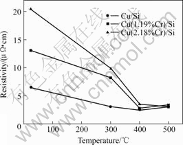
ͼ6 ��Ĥ��ϵ���������˻��¶ȵı仯����
Fig.6 Resistivity variation of systems upon annealing at various temperatures
�������������ƽ�����ɳ̦�eff�ɷ��ȡ�������Ĥ�еĦ�eff��������ʽ��ʾ[15]��
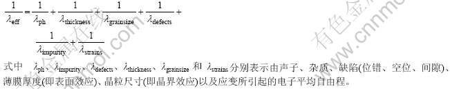
�����£��ڿ��嵥�������У�����ɢ��������Ҫ�����أ������ڱ�Ĥ״̬�£��κ����������ض����ܳ�Ϊ��Ҫ�����ء�����̬Cu(Cr)�Ͻ�Ĥ���ھ�������ȫ�������ߴ�С����Ĥ�ڵ�ȱ�ݺ�Ӧ������Ӱ�����ӣ�ʹ�ñ�Ĥ�ĵ�����Զ���ڴ�ͭ��Ĥ�ĵ����ʡ������ɢ�˻�֮����Scherrer��ʽ[16]��֪����Ĥ�����ߴ�����������С��ͬʱ�ڱ�Ĥ������������ڵ��ӡ����ӻ�ԭ�Ӻ������ĵ���ȱ��Ũ�ȵļ�С�Լ��˻�ʱ�Ͻ�Ԫ�ص���ɢҲ����������Cu(Cr)��Ĥ�ĵ����ʡ��˻��Ĵ�ͭ��Ĥ���Ա���ȱ��Ũ�Ƚ���������ĵ������½��ij̶ȣ���Cu(Cr)��Ĥ�˻��ʣ������ʵ����Ӳ�����ȫ�ǻ�����ʣ��Ͻ�Ԫ������ģ��Ͻ�вĽ�������д����ĸ����ȱ��Ҳ����������Cu(Cr)��Ĥ�ĵ����ʡ�
����������Cu(Cr)�Ͻ�Ĥ��Cu��Ĥ�������Ե����ƣ���Ϊ���ɵ�·���»������Ͼ���һ����DZ�����ơ�һ��ȷ�����ʵĺϽ�Ԫ�غ����Լ��������˻�����ʹ�Ͻ�Ԫ��Cr�ܹ���ȫƫ�ۣ����ҽ��͵���ȱ��Ũ�ȣ�Cu(Cr)��Ĥ���ܹ����ֳ����õ�����������������õ�Ӧ�á�
3 ����
1) ��Cu/Si��Ĥ��ϵ��ȣ�Cr�ļ�����ǿ�˽���̬ͭ��Ĥ��(111)֯����I(111)/I(200)�ֱ�ߴ�4.69 (Cu(1.19%Cr)/Si)��3.91 (Cu(2.18%Cr)/Si)������˻��Cu(200)��Cu(220)��������˻��¶����߶���ǿ������Ĥһֱ���ֽ�ǿ��(111)֯����Cu(Cr)��Ĥ(111)֯������ǿ�Լ�Cu(200)����γ��뱡Ĥ�����ܵļ�С�Լ�����ԭ����ɢǨ����ɵ�Ӧ���ܵ������йء�
2) Cr���������������Cu/Si��Ĥ��ϵ�����ȶ��ԡ�500 ���˻�30 min��Cu��Ĥ�������ܶȼ�ƽ�����½����ṹ���ɣ�Cu��Ĥ�����������ԵĻ���ɢ����Cu(Cr)��Ĥ��һֱ���ֽϸߵ����ܶȣ����ȶ���������ߡ�
3) Cr���������ӽ���̬Cu��Ĥ�ĵ��衣���˻��¶ȵ����ߣ�Cu(Cr)��Ĥ�������ȼ�С��������Cu(1.19%Cr)��Cu(2.18%Cr)��Ĥ��400 ���Լ�500 ���˻�30 min������ʷֱ�ﵽ��Сֵ2.76 �̦�?cm��2.97 �̦�?cm����Cu��Ĥ���(2.55 �̦�?cm)���˻�ʱCu(Cr)��Ĥ�����ʵĴ���½��뱡Ĥ�����ߴ������Լ��Ͻ�Ԫ�ص��ٷֲ��йء�������Cr�����Լ��������˻���ʹ��Cu(Cr)��Ĥ��Ϊ���»����߲��ϵ�Ӧ�þ���һ����DZ�����ơ�
REFERENCES
[1] Lin X W, Pramanlk D. Future interconnect technologies and copper metallization[J]. Solid State Technology, 1998, 41(10): 63-79.
[2] Hu C K, Harper J M E. Copper interconnections and reliability[J]. Materials Chemistry and Physics, 1998, 52(1): 5-16.
[3] Harper J M E, Rodbell K P. Microstructure control in semiconductor metallization[J]. J Vac Sci Technol, 1997, B15: 763-779.
[4] Barmak K, Lucadamo G A, Cabral C Jr, Lavoie C, Harper J M E. Dissociation of dilute immiscible copper alloy thin films[J]. Journal of Applied Physics, 2000, 87(5): 2204-2214.
[5] Gungor A, Barmak K, Rollett A D. Texture and resistivity of dilute binary Cu(Al), Cu(In), Cu(Ti), Cu(Nb), Cu(Ir), and Cu(W) allow thin films[J]. J Vac Sci Technol, 2002, B20(6): 2314-2319.
[6] Liu C J, Jeng J S, Chen J S, Lin Y K. Effects of Ti addition on the morphology, interfacial reaction, and diffusion of Cu on SiO2[J]. J Vac Sci, 2002, B20(6): 2361-2366.
[7] Hong S J, Lee S, Yang H J, Lee H M, Ko Y K, Hong H N, Soh H S, Kim C K, Yoon C S, Ban K S, Lee J G. Effects of the dissolved oxygen in Ti films on Ti reactions in Cu/Ti/SiO2/Si system upon annealing[J]. Semicond Sci Technol, 2004, 19(11): 1315-1321.
[8] Kim J, Wen S H, Yee D. Coevaporation of Cr-Cu and Mo-Ag[J]. J Vac Sci Technol, 1988, A6(4): 2366-2370.
[9] Cabral C Jr, Harper J M E, Holloway K, Smith D A, Schad R G. Preparation of low resistivity Cu-1%Cr thin films by magnetron sputtering[J]. J Vac Sci Technol, 1992, A10(4): 1706-1722.
[10] ���½�, ������, ������, �� ��. ���дſؽ���Cu1-xCrx (x=1.19~2.37)��Ĥ���Ʊ�[J]. �й���ɫ����ѧ��, 2006, 16(11): 1876-1881.
WANG Xin-jian, JIANG Chuan-hai, WANG Jia-min, HONG Bo. Preparation of Cu1-xCrx(x=1.19-2.37) films by magnetron sputtering a single target[J]. The Chinese Journal of Nonferrous Metals, 2006, 16(11): 1876-1881.
[11] Detavernier C, Deduytsche D, van Meirhaeghe R L, de Baerdemaeker J, Dauwe C. Room-temperature grain growth in sputter-deposited Cu films[J]. Applied Physics Letters, 2003, 82(12): 1863-1865.
[12] Ko Y K, Jang J H, Lee S, Yang H J, Lee W H, Reucroft P J, Lee J G. Effect of molybdenum, silver dopants and a titanium substrate layer on copper film metallization[J]. Journal of Materials Science, 2003, 38(2): 217-222.
[13] Kazutomo H, Yoshiaki I, Ken-Ichi H. Diffusion of vanadium, chromium, and manganese in copper[J]. Metallurgical Transactions A, 1977, 8(3): 469-472.
[14] Lee W H, Ko Y K, Jang J H, et. al. Microstructure control of copper films by the addition of molybdenum in an advanced metallization process[J]. Journal of Electronic Materials, 2001, 30(8): 1042-1047.
[15] Hall P M, Morabito J M, Poate J M. Diffusion mechanisms in the Pd/Au thin film system and the correlation of resistivity changes with Auger electron spectroscopy and Rutherford backscattering profiles[J]. Thin Solids Films, 1976, 33(1): 107-134.
[16] Guo Z, Keong K G, Sha W. Crystallization and phase transformation behavior of electroless nickel phosphorus platings during continuous heating[J]. Journal of Alloy and Compounds, 2003, 358(2): 112-119.
������Ŀ���Ϻ�Ӧ�ò����о���չ����������Ŀ(0525)
�ո����ڣ�2007-04-17�������ڣ�2007-08-22
ͨѶ���ߣ����½�����ʿ�о������绰��021-54747441��E-mail: xinjian_wang@sjtu.edu.cn
ժ Ҫ�����ü��Ͻ����Si(100)�ĵ״ſؽ����Ʊ�Cu��Cu-1.19%Cr��Cu-2.18%Cr��Ĥ���о�Cr��Cu��Ĥ��300~500 ������˻�ǰ��Ľṹ�͵����ʵ�Ӱ�졣X�����������������Cu��Cu(Cr)��Ĥ������Cu(111) ��Cu(200)����壬����Cu(Cr)��Ĥһֱ���ֽ�ǿ��(111)֯����ԭ����������������Cu��Ĥ��500 ���˻�ʱ����Ĥ�����������ԵĻ���ɢ����Ĥ��������ܶȼ�ƽ�����½�����Cu(Cr)��Ĥ���˻�ʱ���ֽϸߵ����ܶȣ�Cr�������Cu/Si��Ĥ��ϵ�����ȶ��ԡ�Cu(Cr)��Ĥ�ĵ��������¶������ȼ�С�������ӣ���400 �漰500 ���˻�30 min��ֱ�ﵽ��Сֵ2.76 �̦�?cm��2.97 �̦�?cm���봿CuĤ���(2.55 �̦�?cm)��Cu(Cr)��Ĥ�˻�����ʵĴ���ȼ�С�뱡Ĥ�����ߴ�������Լ�Cr����ɢ�йء�������Cr���Ӻͺ������˻���ʹ��Cu(Cr)�Ͻ�Ĥ�ڸ��»������Ϸ�����кܴ��Ӧ��ǰ����
