

Fabrication and structure characterization of ITO transparent conducting film by sol-gel technique
LI Zhi-hua(��֥��)1, REN Dong-yan(�ζ���)2
1. School of Materials Science and Engineering, Central South University, Changsha 410083, China;
2. Department of Materials Engineering, Mianyang Vocational and Technical College, Mianyang 621000, China
Received 20 July 2006; accepted 4 April 2007
Abstract:
Using In(NO3)3?5H2O and acetylacetone as raw materials and anhydrous SnCl4 as dopant, the transparent conducting indium tin oxide(ITO) films were prepared by sol-gel and dip-coating technique. The phase transformation, structure properties and physical properties (sheet resistance and transmittance) of the films were investigated by DTA-TG, XRD, SEM, four-probe method and UV-Vis spectrometry. The results indicate that it is feasible to fabricate ITO films on the quartz substrates by sol-gel technique, and the ITO films are formed by accumulating of particles with the size of several decades of nanometers. The prepared ITO film has cubic bixbyite structure, and (111) is its preferred plane. After five-times dip-coating, the ITO film has a thickness less than 150 nm, a sheet resistance of 110 ��/��, a resistivity of 1.65��10-3 ��?cm and a transparency of 90%.
Key words:
indium tin oxide; sol-gel; structure characterization; fabrication;
1 Introduction
Since the first sheet of transparent conducting membrane was prepared by using spraying hot Gd2O3 in 1907, transparent conducting membranes have been widely applied in thin film transistor(TFT) and liquid crystal display(LCD), etc. At present, transparent conducting indium tin oxide (ITO) membranes have not only good electrical conductivity, but also eminent transparency for visible light. And due to its easy machining performance, high film rigidity and fine resistance to abrasion and erosion, ITO membranes are broadly used in many fields such as TFT[1-2], LCD[3-4], active and passive components of photovoltaic device[5-6] and infrared radiation in recent years[7].
Among various methods for the preparation of ITO membrane, the widely used ones are magnetron sputtering method[8-10], activated reactive evaporation method[11-12], chemical vapour deposition method [13-14] and recently developed sol-gel process[15-18]. Sol-gel technique attracts broad attention because of its low cost, simple facility, controllable technique and possibility for the preparation of large area membrane compared with other methods. And ITO conductive membranes prepared by sol-gel method have commonly low electrical resistivity. However, sol selection and influence of specific technique condition on the film performance during the preparation process still need studying.
In this paper, the preparation technique of ITO membrane was studied. DTA-TG, XRD, SEM, four-probe resistance apparatus, and UV-Vis spectrophotometer were employed to investigate phase transformation process, structures and physical properties of the phases and films.
2 Experimental
Pure In(NO3)3��5H2O, acetylacetone and diethylene- triamine(DTA) as stabilizer were mixed in a tri-orifice flask at room temperature, and then stirred at 60-65 �� for 3 h to obtain a homogeneous and stable sol. Then SnCl4 ethanol solution was added into the sol according to adulterated concentration, and stirred for 5-10 min to be uniform. So ITO sol with various tin-doping ratios was obtained. Cleaned and dried quartz glasses with the size of 30 mm��20 mm��3 mm were selected as substrates. ITO films were prepared with drawing technique.
Phase transformation processes were investigated by PTC-1 type thermal analyzer. Changes of crystallization and phases of the ITO films treated at different temperatures were analyzed by X-ray diffraction (SIMENS D500X). Meanwhile the physical quantity �� was calculated using mathematics process to the strongest diffraction peak by the INSTR-ST program. Resistivities of the films were measured with WS-1 four-probe apparatus. Their transparency was detected by TU-1800SPC type UV-Vis spectrophotometer. Micro- structure, morphology, thickness and adhesion to the substrates were also studied by KYKY-Amray 2800 type SEM. Qualitative analysis of chemical components and adhesion to the substrates were investigated by EDS matched to the SEM.
3 Results and discussion
3.1 Transformation from gel to crystal
Fig.1 shows DTA��TG curves of ITO xerogel powder dried at 100 ��. It can be seen from this figure that there are three transformation points in the DTA curve, 335.37, 483.05 and 578.21 ��, respectively. The DTA curve shows an exothermic peak at 335.37�� and another obvious exothermic peak at 483.05 ��. From the related TG curve, it can be seen that mass loss rate of ITO xerogel powder is 15.9% from room temperature to 335.37 ��. This is caused by the charring process of remaining organic substance in the gel. The mass loss rate from 336.37 �� to 529 �� is 22.8%. It mainly results from the oxidation of carbon and intermolecular dehydration of indium hydroxide in the gel. Both of them are typically exothermic reactions.
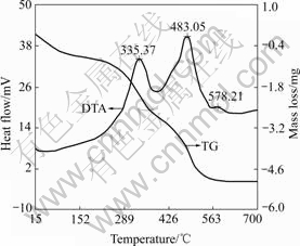
Fig.1 DTA��TG curves of ITO xerogel powder dried at 100��
A small exothermic peak at 578.21 �� can also be found, but the mass does not change at this temperature, which is probably resulted from the transformation of In2O3 to cubic bixbyite polycrystalline structure. After the temperature reaches 530 ��, there is no mass loss of ITO xerogel according to TG curve.
Fig.2 shows the XRD patterns of ITO xerogel powder heat treated at 200, 300, 400 and 600 ��, respectively. Transformation from gel to crystal under certain heat treatment condition can be characterized from this figure. Xerogel after heat treatment has obvious cubic bixbyite polycrystalline structure and the most distinctly characteristic peak at (111) plane. When the heat treatment temperatures are above 200 ��, inter- molecular dehydration of xerogel on the substrates starts and characteristic peak of In2O3 appears. The characteristic peaks become more sharp with the increase of heat treatment temperature, indicating increase of crystalline grain size and crystallization degree. Characteristic peaks of cubic bixbyite polycrystalline structure become more obvious after being heated at 300 ��. It can be also seen that the XRD diffraction peaks present visible broadening according to dimensional effect of membrane thickness. Physical quantity �� is calculated by mathematical fitting to the most intensive peak located at (222) orientation through INSTR-ST program of X-ray diffraction instrument. The particle size of ITO membrane heat treated at 600 �� is calculated to be about 20 nm by Scherrer equation, which is in good agreement with that investigated by SEM.
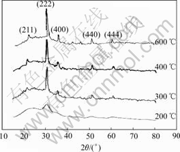
Fig.2 XRD patterns of ITO membranes heat treated at different temperatures
3.2 Morphologies and adhesion to substrates
Fig.3 shows cross-sectional SEM image of ITO conductive and transparent membrane after withdrawing for 5 times. It can be found that the thickness of the membrane doesn��t exceed 150 nm and adhesion to substrate is relatively compact. Fig.4 shows the corresponding surface SEM image of ITO membrane on the substrate. It can be seen that fairly uniform film of sol is formed on the substrate without over large area macroscopic defects such as cavity and air hole. The film has loose structure accumulation of particles with size of several decades of nanometers. Some white larger particles in the figure are supposed to be the deposition of In2O3.
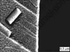
Fig.3 Cross-sectional SEM image of ITO membranes after withdrawing for 5 times
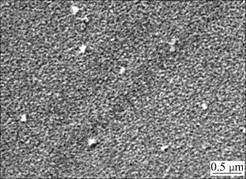
Fig.4 Surface SEM image of ITO membrane
The EDS results of ITO membranes on the quartz substrate are shown in Fig.5. EDS analysis indicates that In and Sn are the main components of the white particles in Fig.4. Chemical bonding between ITO membrane and the substrate may occur and Si��O��In bond is probably formed during the long-time process of heat treatment.
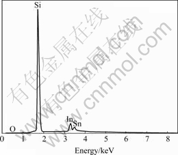
Fig.5 EDS of ITO membranes
At the same time, the Sn element dissolves in crystal lattice of In and donor level is formed for doping effect. Due to the potential chemical bonding, ITO membrane doesn��t fall off and the conductivity of ITO membrane doesn��t change after repeated cleaning.
3.3 Physical properties of ITO films
The resistance of ITO membrane was measured by WS-1 type four-probe electrical resistivity apparatus. After 5 times withdrawing, the membrane has a sheet resistance of 110 ��/��. Since its thickness does not exceed 150 nm according to cross-sectional SEM observation, the resistivity is briefly estimated to be about 1.65��10-3 ��?cm. The fabricated ITO films have sound conductivity.
The conductivity of ITO film is mainly derived from the donor doping effect yielded via replacement of In-ion sites by Sn ions in lattice and the oxygen vacancy caused by heat treatment process. When In2O3 is doped by Sn4+ ions, due to approximate radii between In3+ and Sn4+, In3+ ions are easy to be replaced by Sn4+ ions. The doping reaction can be expressed as
![]()
Bounding to the trapped electron by Sn4+ is relatively weak, hence the electrons can easily escape and turn to be charge carriers.
There is another source of charge carriers in ITO films, namely oxygen vacancies, which are formed during the process of heat treatment because partial oxygen ions in In2O3 deviate from regular location of lattice. The oxygen vacancy is similar to a center with positive charge and can trap electrons, which are shared by neighboring In3+ ions and prone to be excited up to conduction band as energy level of In3+ is just below the conduction band edge. The formation of oxygen vacancy is displayed as
![]()
The visible transmittance of ITO membrane in the wavelength range from 330 to 1 000 nm is shown in Fig.6. ITO membranes by sol-gel possess outstanding transmittance properties within the visible light range. The quartz substrate after 5 times withdrawing has a transmittance of 90% or above in the wavelength range from 500 to 1 000 nm.
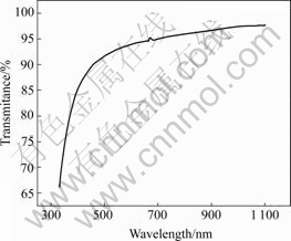
Fig.6 Transmittance of ITO membranes
The prepared ITO films have favorable transparency that is closely related to their valence band structure. ITO film is one kind of wide-band-gap materials whose band gap is between 3.75 and 4.00 eV. The outermost electron orbitals of In3+ ions are 4d10 and the d subshells are fully occupied by electrons. When the band-gap energy is 3.75 eV, wavelength of �ˡ�330 nm can be calculated according to
Eg=hc/�� (3)
where Eg is the band-gap energy, h is the Planck constant and c is the light velocity in vacuum. Therefore, when the visible light with the wavelength longer than 330 nm radiates into ITO films, electrons in the 4d10 full-filled band cannot be excited up to the conduction band by photons because of insufficient energy, thus the ITO films exhibit considerably favorable transparency. The present experiment verifies that ITO films are highly transparent within the visible light range between 400 and 800 nm.
4 Conclusions
1) Transparent conducting ITO membranes were prepared on the quartz substrates by sol-gel technique. Transformation from gel to crystal starts when the treatment temperatures are above 200 ��; this reaction ends when the treatment temperature reaches 530 ��.
2) ITO membranes by sol-gel have loose structure accumulation of particles with the size of decades of nanometers. Chemical bonding between ITO membranes and the substrates occurs and their adhesion is relatively compact.
3) After 5 times withdrawing, ITO membranes have a thickness of less than 150 nm, a sheet resistance of 110��/�� and a resistivity of 1.65��10-3��?cm. Meanwhile, the quartz substrates have a 90% transmittance or above in the wavelength range from 500 to 1 000 nm.
References
[1] IL R J, JIN C Y, KEUN W I, RYU J I, CHOI Y J, WOO I K, LIM B C, JANG J. High performance ��-Si TFT with ITO/n+ ohmic layer using a Ni-silicide [J]. Journal of Non-Crystalline Solids, Part B, 2000, B266/269: 1310-1314.
[2] BISWAS P K, DE A, DUA L K, CHKODA L. Work function of sol-gel indium tin oxide (ITO) films on glass [J]. Applied Surface Science,2006, 253(4): 1953-1959.
[3] SOLIEMAN A, AEGERTER M A. Modeling of optical and electrical properties of In2O3?Sn coatings made by various techniques[J]. Thin Solid Films, 2006, 502(1/2): 205-211.
[4] SON K S, CHOI D L, LEE H N, LEE W G. The interfacial reaction between ITO and silicon nitride deposited by PECVD in fringe field switching device [J]. Current Applied Physics, 2002, 2(3): 229-232.
[5] ISHIBASHI K, WATABE K, SAKURAI T, OKADA O, HOSOKAWA N. Large area deposition of ITO films by cluster type sputtering system [J]. Journal of Non-Crystalline Solids, 1997, 218: 354-359.
[6] SU C, SHEU T K, CHANG Y T, WAN M A, FENG M C, HUNG W C. Preparation of ITO thin films by sol-gel process and their characterizations[J]. Synthetic Metals, 2005, 153(1/3): 9-12.
[7] HATTON R A, DAY S R, CHESTERS M A, WILLIS M R. Organic electroluminescent devices: Enhanced carrier injection using an organosilane self assembled monolayer (SAM) derivatized ITO electrode [J]. Thin Solid Films, 2001, 394(1/2): 291-296.
[8] CANHOLA P, MARTINS N, RANIERO L, PEREIRA S, FORTUNATO E., FERREIRA I, MARTINS R. Role of annealing environment on the performances of large area ITO films produced by RF magnetron sputtering [J]. Thin Solid Films, 2005, 487(1/2): 271-276.
[9] HU Ya-lan, DIAO Xun-gang, WANG Cong, HAO Wei-chang, WANG Tian-min. Effects of heat treatment on properties of ITO films prepared by RF magnetron sputtering[J]. Vacuum, 2004,75(2): 183-188.
[10] DAOUDI K, SANDU C S, MOADHEN A, GHICA C, CANUT B, TEODORESCU V S, BLANCHIN M G, ROGER J A, M. OUESLATI, B. BESSA?S. ITO spin-coated porous silicon structures [J]. Mater Sci Eng B, 2003, B101(1/3): 262-265.
[11] OTA R, SEKI S, SAWADA Y, OGAWA M, NISHIDE T, SHIDA A, IDE M. Indium-tin-oxide films prepared by dip coating using an ethanol solution of indium chloride and tin chloride [J]. Surface and Coatings Technology, 2003, 169/170: 521-524.
[12] SEKI S, SAWADA Y, OGAWA M, YAMAMOTO M, KAGOTA Y, SHIDA A, IDE M. Highly conducting indium-tin-oxide transparent films prepared by dip-coating with an indium carboxylate salt[J]. Surface and Coatings Technology, 2003, 169/170: 525-527.
[13] KIM Y S, PARK Y C, ANSARI S G, LEE B S, SHIN H S. Effect of substrate temperature on the bonded states of indium tin oxide thin films deposited by plasma enhanced chemical vapor deposition [J]. Thin Solid Films, 2003, 426(1/2): 124-131.
[14] LIN H, JIN T, DMYTRUK A, SAITO M, YAZAWA T. Preparation of a porous ITO electrode [J].Journal of Photochemistry and Photobiology A: Chemistry, 2004, 164(1/3): 173-177.
[15] AL-DAHOUDI N, AEGERTER M A. Comparative study of transparent conductive In2O3?Sn (ITO) coatings made using a sol and a nanoparticle suspension[J]. Thin Solid Films, 2006, 502(1/2): 193-197.
[16] ALAM M J, CAMERON D C. Characterization of transparent conductive ITO thin films deposited on titanium dioxide film by a sol-gel process[J]. Surface and Coatings Technology, 2001, 142/144: 776-780.
[17] CHEN Shi-zhu, LI Jing. Sol-gel dip-coating technique for preparation of ITO thin film [J]. The Chinese Journal of Nonferrous Metals, 2005, 15(1): 94-99. (in Chinese)
[18] LI Zhi-hua, REN Dong-yan. Preparation of ITO transparent conductive film by sol-gel method [J]. Trans Nonferrous Met Soc China, 2006, 16(6): 1358-1361.
Corresponding author: LI Zhi-hua; Tel: +86-731-8830838; E-mail: ligfz@mail.csu.edu.cn
Abstract: Using In(NO3)3?5H2O and acetylacetone as raw materials and anhydrous SnCl4 as dopant, the transparent conducting indium tin oxide(ITO) films were prepared by sol-gel and dip-coating technique. The phase transformation, structure properties and physical properties (sheet resistance and transmittance) of the films were investigated by DTA-TG, XRD, SEM, four-probe method and UV-Vis spectrometry. The results indicate that it is feasible to fabricate ITO films on the quartz substrates by sol-gel technique, and the ITO films are formed by accumulating of particles with the size of several decades of nanometers. The prepared ITO film has cubic bixbyite structure, and (111) is its preferred plane. After five-times dip-coating, the ITO film has a thickness less than 150 nm, a sheet resistance of 110 ��/��, a resistivity of 1.65��10-3 ��?cm and a transparency of 90%.
