ϡ�н���2020���3��
ͭ����������Ĥ̫����ص��о���չ
������ ����� ��ѩ÷ ������ ���� �ϻ�
������ҵ��ѧ���Ͽ�ѧ�빤��ѧԺ�������Ƚ����ܲ����ص�ʵ���ұ����Ƚ������۽ṹ�������ص�ʵ����
ժ Ҫ��
ͭ������(CIGS)��̫�������һ�־��и�ת��Ч�ʵı�Ĥ̫�����,ʵ�����Ʊ���CIGS���ת��Ч���Ѵ�22.9%,�ӽ��ھ���������ߵ�ת��Ч�ʡ�ͬʱCIGS��ػ���������ϵ����,����ɱ��ϵ�,����Ӧ�÷dz��㷺���ŵ㡣Ȼ��,����ҵ���Ĵ��ģ������,CIGS̫����ز�����Ч�ʻ����ȶ��������뾧���ش��ڲ�ࡣ��һ������CIGS���Ч��,�Ż��������,�����ز�ҵ����ģ��CIGS̫����ؽ��չ�ıؾ�֮·����ǰCIGS̫����صķ�չȡ�õ��ش�ɾ�,��Ҫԭ���������Ƕ�CIGS����������ԭ���Ľ�һ����ʶ�������ۺϽ�����CIGS̫�������Ϊ��ǰ�ȵ��DZ��������,�ع��˽��ڹ���CIGS���о���չ,��Ҫ������صĻ���㡢���ղ�ʹ��ڲ�ĸĽ�,�������֮��Ĵ����ֶ�,��Щ�����ķ�չ�����CIGS��ص�ת��Ч��,�ƶ������ҵ������,ͬʱ�ڵ��δ����չ����������������,���Խ������������չ����
�ؼ��ʣ�
ͭ������ ;̫����� ;��Ч�� ;��ҵ�� ;
��ͼ����ţ� TM914.42
����飺 ������(1995-),Ů,�ӱ�ʯ��ׯ��,˶ʿ�о���,�о�����:��Ĥ̫����ء�ͭ���������;E-mail:479640028@qq.com;; *�ϻ�,����,�绰:010-67391876;E-mail:hyan@bjut.edu.cn;
�ո����ڣ� 2018-09-20
���� ������Ȼ��ѧ������Ŀ(61574009,11574014)����;
Research Progress of Copper Indium Gallium Selenide Thin Film Solar Cells
Qu Jingjing Zhang Linrui Song Xuemei Zhang Yongzhe Wang Hao Yan Hui
Key Laboratory of Advanced Functional Materials of Education Ministry of China,Beijing Key Laboratory of Microstructure and Property of Advanced Materials,College of Materials Science and Engineering,Beijing University of Technology
Abstract��
Copp er indium gallium selenium(CIGS) based solar cells were thin film solar cells with high conversion efficiency.The conversion efficiency of CIGS solar cells prepared in the laboratory reached 22.9%,which was close to the highest conversion efficiency of crystal silicon solar cells.At the same time,CIGS cells also had the advantages of high absorption coefficient,low manufacturing cost,and wide application.However,in large-scale commercial production,CIGS solar cells were still far from silicon-based solar cells in terms of efficiency and stability.Further improving the efficiency of CIGS solar cells,expanding the scale of cells industrialization and optimizing their performance were the only way for the future development of CIGS solar cells.The main achievements of the current development of CIGS solar cells were mainly due to people's understanding of CIGS materials and device principles.In this paper,the potential and advantages of CIGS solar cells as a hot spot and recent research progresses on CIGS solar cells were reviewed,including the improvement of buffer layer,absorption layer and window layer,as well as the treatment methods between the layers.The development of these technologies improved the conversion efficiency of CIGS solar cells and promoted its industrialization.At the same time,the related problems in the future development of cells and the solutions were discussed.
Keyword��
copper indium gallium selenium(CIGS); solar cell; high efficiency; industrialization;
Received�� 2018-09-20
������ŵ�������Դ����,ʹ������Դ��������˳��㷢չ������,����̫���ܵ���Ч����һֱ��Ŀǰ���о��ȵ�֮һ��������,ʵ����̫����ص�ת��Ч�ʲ���ͻ�������¼,�ڲ�ҵ������,�����������������Ҳȡ���˾������Ŀǰ��ҵ����õĹ����Ʒ�Ǿ����ͱ�Ĥ̫�����,���о����������Ĺ������,����������г���ռ����Ҫ��λ�����Ǿ���,CdTe�Լ�Cu(In,Ga)(S,Se)2 �ȱ�Ĥ��������������Ĺ������Ҳ���ڹ������õ���Խ��Խ������ӡ�����,����Cu(In,Ga)(S,Se)2 (CIGS)�ı�Ĥ̫����������з�չǰ���Ĺ��(PV)��������֮һ,��ʵ���ҹ�ģ�ĵ��ת��Ч���Ѿ��Ȳ����
[1 ]
��
ͭ��������(CuInSe2 ��CIS)��һ�����ڢ�-��-�������Ԫ������,��̫������г�����p�����ղ����,�����ķ���ͭ����ṹ
[2 ]
��1953��,Hahn��
[3 ]
���Ⱥϳ��˴�϶Ϊ1.04 eV��CIS����,֮��ʵ�����Ʊ����ĵ���CuInSe2 ��̫����ص���1974����֤��ת��Ч���Ѿ��ﵽ12%
[4 ]
��1976��,Kazmerski��
[5 ]
ͨ���ڹ�����Se���������¹�����CuInSe2 ��ĩ,�Ʊ����˵�һ��CuInSe2 /CdS��Ĥ̫�����,��ת��Ч�ʴﵽ��4%��5%�������,������˾��������ͨ��ʹ�ù����������Ʊ�����ͭ����(CuInS2 )��Ĥ���,��ȡ����11.4%��ת��Ч��
[6 ]
������ͬһʱ��,Kazmerski��Sanborn
[7 ]
�Ʊ�����Ч��Ϊ3%��CuInS2 ��Ĥͬ�ʽ�̫����ء�CIS�ı�Ĥ̫�������1981�꿪ʼ�õ��˹㷺��ע,���ͬʱMickelsen��Chen
[8 ]
ʹ��Ԫ�ع��������Ʊ����ĵ�ص�ת��Ч�ʴﵽ��9.4%��1987��,CuInSe2 ��Ĥ��س��ڼ�¼��ת��Ч���Ѿ��ﵽ��14.1%
[9 ]
��ʮ���,��1998��,��һ����ҵ����CIGS̫��������Ͷ������
[10 ]
���������Ÿ��ּ�����ͻ��,������(Ga)�IJ�ͬ������,��(Na)����(K)�ȼ��������,����(CdS)���ڲ�ļ���,ͨ�����ӱ����Ͳ�������п(ZnO)��ȵ��Ż�,�ڶ̶̵�ʮ�����,CuInSe��ص�ת��Ч�ʱȹ�ȥ�ļ�ʮ����ߵĻ�Ҫ���ԡ����,ͨ��ʹ�����ӻ������(Zn,Mg)O/Zn(O,S,OH)�Ʊ���Cu(InGa)Se2 ���,���ת��Ч���Ѿ��ﵽ��22.8%
[11 ]
,ʵ�����Ʊ���CIGJS���ת��Ч���Ѵ�22.9%,�ӽ��ھ���������ߵ�ת��Ч��
[12 ]
��
CIGS��Ĥ�Ĵ�϶����ͨ����Gaȡ��In������,���ʹ����Ը��õ�ƥ��̫�����ס�����CIGS��һ��ֱ�Ӵ�϶����,���нϸߵ�����ϵ��,��1��m��ı�Ĥ�������մ�̫������,Լ2.0��2.5��m�ı�����������������豸����Ҫ����Ϊ�ϱ������ղ���Լ���ԭ���ϵ�ʹ��,���Կ�����Ч�ؽ��ͳɱ���ͨ��Ӧ�ø��ֲ�ͬ�ij�������,CIGS���Ͽ��ڸ����Լ����Ի����ϳ���,����CIGS̫����ص�Ӧ�ÿ��Ա鼰������档���ҳ��˵���Ӧ��,CIGS̫�����������߷���������Ҳ�����ڿռ��豸�ϡ�����,���ڵ���Ʊ��IJ������,���CIGS�����ڵ�Ƭ����,�������Խ�һ�����������ɱ�
[13 ,14 ,15 ,16 ,17 ,18 ,19 ,20 ]
��
��ȻCIGS��Ĥ����ŵ��ڶ�,���Ƕ�����Ľ�һ����ҵ��,Ŀǰ�Դ��ڲ�������,���������Ʊ�������ÿ�����еijɷ־����Ծ�����һ,���������й��̿�����,һ���걸��ԭλ��Ϲ�����������Ҫ�ġ�ͬʱ,����CIGS̫����ش��ģ����Ķ�Դ�����������ι����豸�ı�����һ���dz��ؼ������ơ���͵�����Ŀǰʵ����С�����ص�Ԫ(>22.9%)�����۵��ģ��(16.1%)֮��Ч�ʲ��ܴ���,������������,�����ܻ�������Ĺ�Ӧ����,���������ɱ��ļ�������(����1 GW��������Ҫ31 t��)
[21 ]
��
CIGS�������õĹ�������Լ������ڴ��ģ�������Ʊ���������������Ϊ���ͱ�Ĥ̫����ص�DZ�������ơ���ǰCIGS̫����صķ�չȡ�õ��ش�ɾ�,��Ҫԭ���������Ƕ�CIGS����������ԭ���Ľ�һ����ʶ,���ľͶ�CIGS̫����ػ����,���ղ�ĸĽ�,���ڲ�ͽ��洦�������ȷ��������ϸ���ܡ�
1 �ṹ���ص�
1.1 ���Ͻṹ
CIGS����ɲ���CuInSe2 ��CuGaSe2 ���ڢ�-��-���廯����,�����ķ���ͭ����ṹ
[22 ]
�������ķ���ͭ��ṹ��ͨ��I��(Cu)�͢���(In��Ga)Ԫ�ض�II��Ԫ��(Zn)������ȡ��,�ɢ�-�������(ZnSe)����������п��ṹ�ݱ����,ÿ����(Cu)���(In)��ԭ�������ԭ��(Se��S)�γ��ĸ�����������ķ�������,��������(c/a)�ӽ���2,����Cu-Se,In-Se��Ga-Se����ǿ�Ȳ�ͬ,ͬʱ������ɾ���ƫ��(��Ϊ�ķ�����)��
1.2 CIGS�ṹ
CIGS��Ĥ̫����صĻ����ṹΪ�ĵ�/Mo/���ղ�/�����/�����/���ڲ�/������/����դ��
[23 ,24 ,25 ]
���ĵ�����ͨ�ĸ����ƸƲ���(SLG),��Ϊ������Ϊ��Ч����ṩ���Խ���Ԫ��,ͬʱ�����нϺõ����ȶ��Ժͻ�ѧ����,�����ղ����Ƶ�������ϵ��,���������⻬������,����������Ե����,Ҳʹ�ò���ֲ�Ƭ������ǰ�(PI)��Ϊ���Գĵ�,�������CIGS�ྦྷ��Ĥ̫�����
[23 ]
����������ս��䷽ʽ�ڳĵ��Ͻ���һ��Mo,��Ϊ��صı��缫,������Ѩ�����缫�ĺ��һ����0.5��1.0��m,�Ա�֤�缫����ĵ�֮��������õĸ�����,ͬʱ���������ղ��γ����õ�ŷķ�Ӵ����ڱ��缫�Ͽ��Բ�����ջ��߷����(��ѧˮԡ������)���յõ�һ����Ϊ1��3��m��p��CIGS���ղ�ͺ��Ϊ0.03��0.05��m��n��CdS��������������ʽᡣ�ڻ������������Ƶ��ֱ���ſؽ����Ʊ�������������(TCO)����Ϊ���ڲ�,Ŀǰ�����Ĵ��ڲ���Ҫ��һ�㱡�ı�������п(i-ZnO,0.05��m)�������ӵ�����п���(ZnO:Al,0.1��0.3��m)
[26 ]
�������������ڷ�ֹ����ֲ��IJ������Ի������Dz���ȫ���µķ�Χ�ڵ�©����
[27 ,28 ]
,Ҳ���Ա����������TCO�����ڼ������������ˡ�
1.3 CIGS��Ĥ�����c-Si��صıȽ�
SiԪ����һ�ִ����ḻ��Ԫ��,�ڵؿ��еĺ�����������,ռ�ؿ���������26.4%,��������̫����ص���Ҫ���ϡ�������ڹ��̫�������˵,CIGS��ԭ���ϴ������١�����Ϊ�˻�ø����պ�еǿ�ȵ����,���̫�����ģ�������о���ʹ�ýϺ��c-Si��Բ(180 mm)��Ϊ���ղ�,��ͻ���ɵ�������ɱ���Լ50%��Ϊ���Ʊ���c-Si��Բ,ͬʱc-Si̫�������Ҫ������ߴ�Ĵ�Si����,��͵������������հ�����SunPower��������NREL��֤��c-Si������ת��Ч���Ѿ��ﵽ��24.1%(���11310.1 cm2 )��������CIGS̫�������˵,���Ч��ԼΪ16.1%,Զ����c-Si��ص�Ч�ʡ�Ŀǰ�г��ϴ�Լ92%����ҵ���Ϊc-Si��Ʒ,��Ĥ�����ռ8%,������CIGS�����Ϊ2%
[29 ]
��Si��̫����صĿɿ������κ�����̫����ؼ����������,Ŀǰ�Ѿ������˳���Ĺ��ռ�����ͬʱ,c-Si̫����ص������Ѿ���֤�����Դﵽ�����ȶ�(��Լ20��)��������CIGS���,��û���㹻�ɿ����ȶ��Ա�����Բο���
CIGS̫�������Ϊ��̫����ص��������Ʒ,��Si��̫��������,��Ȼ���кܶ����ơ��������Si��̫�����,CIGS��ز����ܵ���,ͬʱCIGS�����ʹ���˶��ֹ��ܲ�,�����ڼ��ٶ�·����(Jsc )��ġ���ǰCIGS��ص��Ʊ���������ܶ�,ͬʱ�漰��ԭ���ϡ��ɱ����Ʊ�ʱ�䶼�Ƚ��١�CIGS��Ĥ����ֱ�ӳ����ڸ��ֳĵ���,��Si������������и����,��Ҫ���ĵ��������١������������,CIGS�����Ҫ���¶�(Լ550��)��c-Si���(Լ1100��)Ҫ��,����CIGS��ؿ����ڵ�ش��������е�Ƭ����,����Si��̫�������,��Ƭ�����Dz�����ʵ�ֵġ��ڳ����c-Si̫�������,Ϊ�˻��ŷķ�Ӵ������ʹ�������,˿��ӡˢդ�ߵ缫�ͱ����Al�Ӵ��ֱ���ҪԼ20��40��m��,����CIGS̫�������,�Ӵ���ȱ�c-Si̫�����ҪС��
����SiΪ��Ӵ�϶����,������������ϵ���ܵ�(1��104 cm-1 )����CIGS��Ϊֱ�Ӵ�϶����,������ϵ���ϸ�,���CIGS���ղ�ĺ�ȿ��Ա�c-Si��Ƭ�ĺ��СԼ100��,�Ӷ�����������ԭ������������,CIGS��������ԴͶ�ʻ�����(1��)Ҫ����cSi����(2��)
[30 ]
���������������������Դ����ϵ�,CIGS̫����ص������ɱ�����Si̫����ء�
��c-Si̫�������,ͨ��������p��c-Si�Ͻ���Si��Ƭ�ı���������泡,����p��c��Si��Ϊ�ز����������ز������͵Ͳ�����֮��ĺ���������(p+ -p��,��Ϊ��-�ͽ�)��������-�ͽ�ĵ糡ʹ����Զ��Ӵ���/����,��˼����˱���ĸ��ϡ����Ƶ�,��CIGS�ı���(����CIGS/Mo����)��GaŨ�ȵĽ�����������泡,���ҵ���Զ�뵽��Mo�����㲢�ҳ���ǰ����,�ɴ������ռ�Ч�ʡ���ʵ���ҹ�ģ(2 cm��2 cm),CIGS̫����ص�Ч���Ѿ��dz��ӽ�c-Si(CIGS22.9%,c-Si 25.6%)��
2 �����о�����չ
2.1 ���ղ�
2.1.1 ���������
���ղ�����Ԫ�صIJ���һֱ��CIGS̫������о����ȵ㡣���������ͨ���ɲ����ĵ���ɢ(Ԥ����)
[31 ]
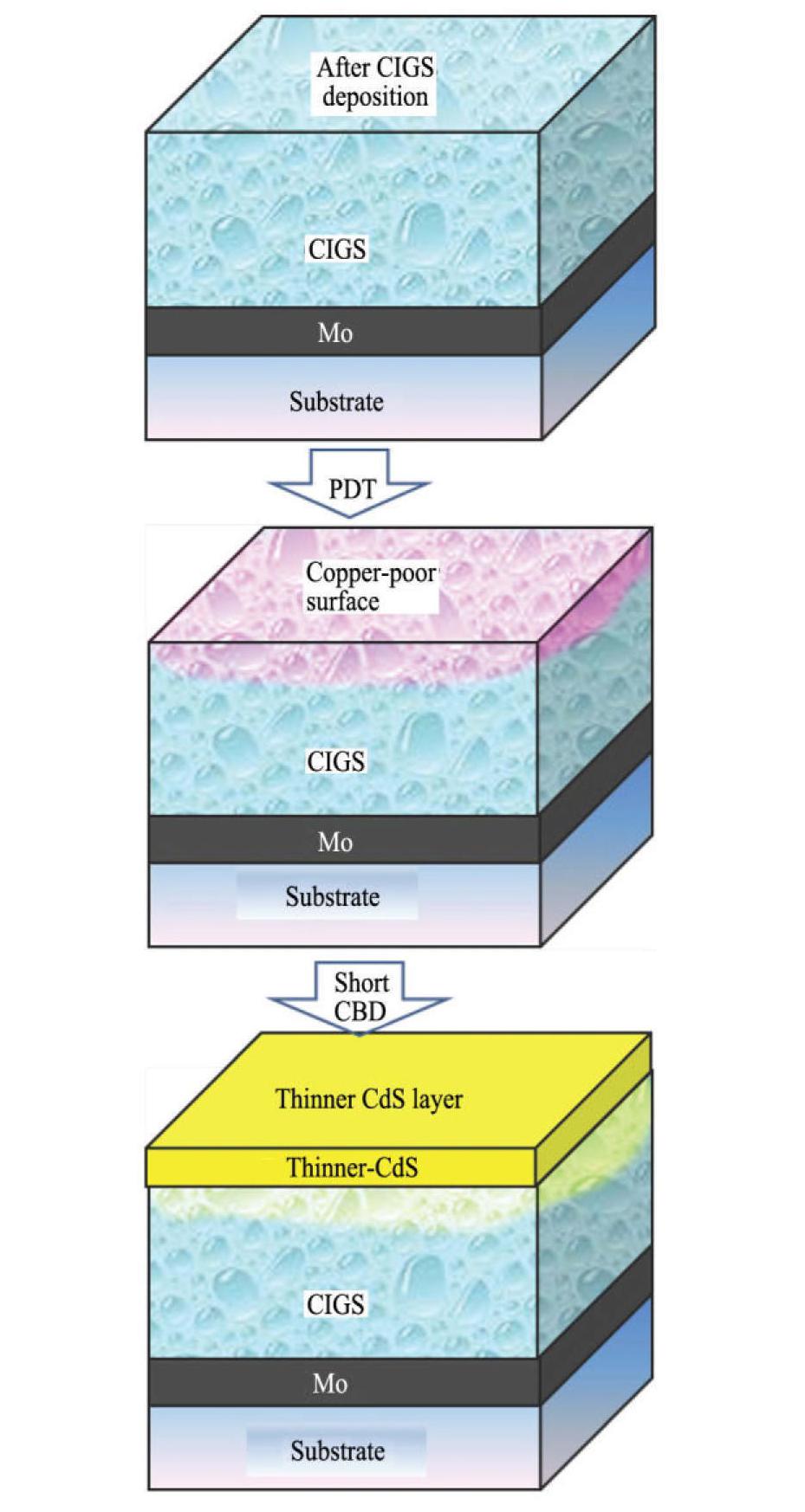
,������CIGS������֮ǰ���ڼ��֮�����ܿصķ�ʽ(Ԥ����,������,�����)���ӡ����Ƿֱ��Ӧ�ż��������ļ����Ǽ�����ĵ�ĵױ������ɢ,���ղ���������й�����,�������ղ��Ʊ�����������������˻�(Ҳ��ΪPDT����)����,��Щ���ӷ�ʽ����Ե�����ʲ�������Ӱ��
[32 ]
��
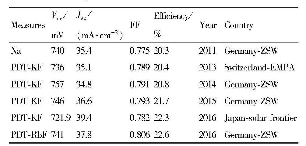
Ԥ��������һ������CIGS���Ʊ�������,Na���ƸƲ����ĵ��ڲ���ɢ�õ�,���Ƕ��ڴ��ģ���,Na�����ͷֲ��ľ����Ի����������Ӱ��,���������Ч�ʡ�����ͨ����Ҫ�ڲ����ĵ��ϳ���һ���������������赲��,���Ʊ���Na��Mo(MoNa)���Ӵ�,ʵ��Na�ľ��ȷֲ�;����Mo���Ӵ��ϳ���һ��NaFǰ���,ȷ�����ղ�����ڼ�Na�ij��㹩Ӧ��Na��������NaF��ĺ�ȿ���,NaF������ᵼ�¿�·��ѹ(Voe )���������(FF)����,������ᵼ�����ղ���������з�������,���һή��̫����ص����ܡ�������Ĺ�����ͨ��ʹ�������ι����������Ʊ�CIGS��Ĺ����С��о�����,�ڵ�һ�͵ڶ��β���Na��ʹCIGS�ᾧ�Ƚ���,�ڵ����εIJ������Ӱ��Ĥ����Ľᾧ��,������Na����Ʒ��ʾ�ϴ�ľ����ߴ��û�зֲ㡣PDT�����Բ��Ӽ������Ũ�����Ʋ���,���ڷ����ھ�������֮��,���PDT���̿��Զۻ�ȱ�ݶ���Ӱ��ᾧ��,����������CIGS̫����ص����ܡ������������¼Ч�ʵ�CIGS̫�������,�����¼Ч�ʵ��ʹ����KF��RbF����������ķ��������1��ʾ,��2011�굽2016��,CIGS��ת��Ч����20.3%�ﵽ��22.6%��KF��PDT����������ʵ������ȡ���˳ɹ�,�����Ѿ���ʼ��չ������ҵ��ص������С������PDT���뵽CIGS����жԵ�ر����Լ����ܲ����Ļ�����������:
(1)��Ч����CdS����,ͬʱ����Jsc��
Chiril����
[34 ]
��X���߹��������(XPS)��������Cu��Ga��CIGS�����ϵ���30 nm��Ⱦ��Ѿ��ľ�,�����CIGS�����ԭʼ�����λ������(OVC)������,����ȱ��Cu ʩ����ʹ�ü����PDT�IJ���ʩ���ܶȸ���û��ʹ��PDT�IJ���,��ᵼ�±��淴Ӧ��ǿ��,�Ӷ���ǿ����ص�ͬ�ʽᡣ�����ͼ1��ʾ,�ڽϺ��ƶͭ�������м����PDT������,�������Ӻͷ��͵�������,������������������,���Ͻ���,����������ܶ�����,Voe ����,����ֻ��Ҫʹ�úܱ��ĵĻ����Ϳ����γɸ�������CIGS/CdS���ʽ�,ͬʱ��������Jsc ������,��ͼ2��ʾ,����ʹ��KF-PDT����Ʒ,CdS����CBD�����ڽα��ֳ����õĸ������;�����
[40 ]
,���CdSĤ���Ը���,�������ڶԶ̲������յ�����,�Ӷ�����Jsc ��
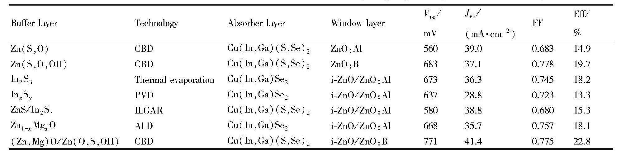
��1 ���ڲ�ͬ��������ӶԵ�����ܵ�Ӱ�� ����ԭͼ
Table 1 Effect of recent alkali metal doping on solar cell performance
[33-39]
ͼ1 PDT�������ʹ�ø����Ļ����
Fig.1 A thinner buffer layer being used after PDT treatment
ͼ2 ��PDT��Ʒ��PDT��Ʒ����CdS�IJ���
Fig.2 The differences in CdS surface between no-PDT samples(a)and PDT samples (b)
[40]
(2)��Ч����CIGS������Ŀ�ѨŨ�� [41,42]��
��ͼ3��ʾ
[42 ]
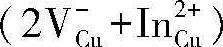
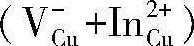
,����PDT��Ʒ,���PDT��Ʒ���,CIGS�����洦�Ŀ�Ѩ������Ũ���������ӡ�NaF-PDT��Ʒ��������Ũ�ȱ�(NaF+KF)-PDT��Ʒ��Լһ��������,ͬʱҲ����KF-PDT��Ʒ��������Ũ�ȡ���Ч��ص�CIGS���ղ������OVC��ɡ�������dz����ȱ��Cu ),�Ӷ����CIGS���еĿ�Ѩ������Ũ�ȡ�Na������ռ��In��λ(VIn ),�γɱ�+ ������O2 ,��Se��λ(Vsc )ת����Osc (Se��O���),���ή�Ͳ�������Ũ�ȡ���������,Na����ʹCIGS������Ŀ�ѨŨ�����ӡ�
(3)ʹCIGS�����϶�����Ҽ۴����͡�
Handick
[43 ]
����PI�ĵ��ϳ�����CIGS���ղ�ı���������ܴ��ṹ����,����NaF-PDT��Ʒ�Ľ������϶Ϊ1.61 eV(+0.14/-0.51 eV),(NaF+KF)-PDT��Ʒ�Ľ������϶Ϊ2.52 eV(+0.14/-0.51 eV),�۴����ֵ(VBM)�����EFλ�������Ե����ơ�Handick��
[43 ]
����˱����϶�����������ڲ��Ͻṹ�仯����ĵ��ӽṹ�ı仯�������������,��������Ҫ��K,In��Se���,��In2 Se3 ������Ĵ�϶�������Եĺ��������,���ڵ�ǰ�Ĵ�϶����,���������������ֻ�����,�����ֻ�������ܹ���,�������в���ȷ������(NaF+KF)-PDT��Ʒ��VBM��������,��NaF-PDT��Ʒ��VBMƫ������,���ҿ�ѨŨ���ںܴ�̶��Ͻ���,�ʽ��渴�Ͻ�һ������,Voe ��ת��Ч��������ߡ�
ͼ3 ͨ��C-V������õĿ�ѨŨ��(N)�ڲ��Ϻ��(W)�ϵķֲ�
Fig.3 Distribution of hole concentration (N) on material thickness (W) obtained by C-V measurements
[42]
(a) No-PDT samples;(b) PDT samples
2.1.2 GaԪ�ص��ݶȷֲ�
CIGS��Ĥ�Ĵ�϶����ͨ������ȡ����������,CIGS���������ķ�չDZ���������϶�Ŀɵ����ԡ�Ga����CIS����Ҫ�ı䵼����λ�ôӶ�������϶������Ga/(Ga+In)�ı��ʸı�,CIGS�Ĵ�϶���Դ�1.04 eV���ӵ�1.67 eV
[44 ,45 ]
�����ڹ̶���϶�뵼����϶�̫���������ղ����,С�ڹ̶���϶�Ĺ����������ܲ�������-��Ѩ��,�ͻᵼ��һ����̫����������������,�Բ��ϵĶ�·������������Ӱ��;�����ڹ̶���϶�Ĺ�������Ҳֻ�ܲ���һ������-��Ѩ��,���������ת��Ϊ������������������CIGS����в��øı�Ga���ݶ��γ��ݶȴ�϶���Ը��ӳ�ֵ�����̫�����ס����ݶȴ�϶������ľ��Ƿ����ݶȴ�϶(���ղ��϶��ǰ�缫�缫�����Լ�С������)�������ݶȴ�϶(���ղ��϶��ǰ�缫�缫���������������)���ڷ����ݶȽṹ��,���ӻ�������ɼ۴�ԾǨ������,����������б,��ʹ�����ɸ�����������������˶�������ռ�����(SCR)�е��ӷ������˶������෴,����һ�����ڽ��糡�����෴�ĸ��ӵ糡,�ᵼ��(1) SCR���ܳ�ǿ����,�����������ӷ���;(2)�����ղ���������������SCR�ļ��ʽ���,���缫�����ϼ�����ǿ�����,���ֽṹ�������ڵ���й��������ӵ��ռ�,����Ӱ���ص�Jxc ���������ݶȽṹ��,�������ܵı仯,������״�Ĵ�϶ͬ�����γ�һ�����ڽ��糡������ͬ�ĸ������糡,�����ڹ��������ӵķ���,ͬʱ���ܼ�С���ӱ����ϵļ��ʡ����������ݶ�б�ʵ�����,���缫���ĸ�������,����Լ�ǿ�����������������ӵ��ռ�����,��ͬʱҲ�ᵼ�������Գ����ι����յļ�С��Ϊ�˼��������������,��CIGS����г����þ��и����չ���˫�ݶȴ�϶,����ĿǰCIGS̫�����������Ч�Ľṹ
[46 ,47 ,48 ]
��CIGS̫����ص�˫�ݶȴ�϶ʾ��ͼ��ͼ4��ʾ,���С�g1 ,Eg2 ,Eg3 Ϊ���ϲ�ͬλ�õĴ�϶��
ͨ�����ι��������������Ʊ�������˫�ݶȴ�϶��CIGS��Ĥ,�䵼�����ݴ�(ȱ��)�������ղ�ǰ����,�˴���϶��խ(Ga%�ϵ�),�����ղ��������Ĵ�϶�Ͽ�(Ga%�ϸ�),�Ӷ�ʹ��Eg3 >Eg1 >Eg2 ������˫�ݶȴ�϶��CIGS̫�����,��SCR�е�ǰ���ݶȿ�����Ч�ؽ���CIGS/CdS����ĸ���,���ݶ�ͨ�����ٱ��渴�Ϻ�������Ч��������ɢ�������յ������糡,�Ӷ�DZ�ڵ���ǿ�������ռ�,ʹ�ö�·�����ܶ�(Jsc )�Ϳ�·��ѹ(Voc )����
[49 ,50 ]
�����������ղ���ͨ������Ga/(Ga+In)�Ŀռ�ֲ��Ϳ��Ե����ܴ������CIGS��ص��������ܡ����,�Ż�Ga/(Ga+In)���������ղ�ķֲ��Ƿdz���Ҫ���о��ȵ㡣Dullweber��
[51 ]
���ö�Ԫ���������Ʊ��������ݶȴ�϶CIGS���,�о������ʾ�����ݶȴ�϶���������Ʊ��缫���ĸ���,����SCAPS��ģ������ʵ������һ�¡�Amin��
[52 ]
�о��˳������ղ��д�϶�ݶȶԵ�����ܵ�Ӱ��,ʵ������ʾ�������Ӧ�ĵ�ؽṹ��Ӧ�������϶�ṹ,�������ܽ��ֱ��10.74%������12.38%,14.36%������17.26%��������ʾ�ڳ������ղ���Ӧ��˫��϶�ṹ�Ǹ��õ�ѡ��,����Ŀǰ���Ʊ�����Ȼ�����ѵ㡣ʵ����,�Բ�ͬ������Ż���һ����ߵ��Ч����Ч�ķ�ʽ
[52 ]
��Jackson��
[37 ]
ͨ�������ղ㶸�͵�Ga/(Ga+In)�ݶȵ��Ż��ͼ����PDT����,ͬʱ����CdS�������,�Ʊ�����ת��Ч�ʸߴ�21.7%��CIGS��ء�
ͼ4 CIGS̫����ص�˫�ݶȴ�϶ʾ��ͼ
Fig.4 Schematic diagram of double gradient band gap for CIGS solar cells
�о��������CIGS�����Ĵ�϶��������������ܷ���������Ҫ������,���Ƕ���CIGS������˵,���ʵ�ֶ�GaԪ�طֲ��ĺ���������Ŀǰ�о����ѵ�,���谭�����һ����չ��Ӧ�á�Ŀǰ���о���Ҫ������ʹ�ö����ֶ�,���ڽ��������ʹ�ö�Ԫ��в�,�ı����������е��¶���ʱ���,������ݶ�CIGS̫�����,�������о����١����,Ϊ�˳������̫������,��CIGS���ղ�Ĵ�϶���̵������о��Ƿdz���Ҫ�ġ�
2.2 �����
CIGS̫�������ͨ��ʹ��CdS��Ϊ�����
[25 ]
��Ŀǰ,CdS������Ѿ�����CIGS̫����صĴ�Ҫ��,�������ղ�CIGS��δ���ӵ�ZnO����к��ʵĵ�����,CIGS��ص��ܴ�ͼ��ͼ5��ʾ��CdS�������������֮���������Ľ���ȱ�ݻ�ѧ,�ݱ���,������ɵ�Cd������ƶͭ�Ļ�ͭ������γ��ȶ���ʩ����ȱ��,���Բ�����ѵĵ���ܶȺ���ȷ�ķ����ܼ�λ��
[53 ]
��CdS��ͨ��ͨ����ѧˮԡ����(CBD)������CIGS���ղ���档CBD��Һһ��Ϊ����ˮ��Һ(pH>9),��Ҫ����3�ֳɷ�:������Ϊ��Դ(CddSO4 ,CDI2 ��),��ˮ(NH4 OH)��Ϊ��ϼ�,������Ϊ��Դ����ˮ��������Ϊ��������(Cdd)�ṩ����,��ͨ��pH�仯���������ˮ�⡣ͬʱCBD��Һ�еİ�������һ���̶��ϸ�ʴCIGS����,�����Ϳ�����CdS�γ�֮ǰȥ���������ʵ�CIGS����(�����������)
[54 ]
��CdS����Ҫȱ��Ϊ����Խ�խ�Ĵ�϶(2.4eV),�ᵼ�µ�ص����ļ���������ʧ,�Լ�Cd�Ķ������⡣���,�����CdS�����ӻ������о��ǵ�ǰ�о��ȵ�֮һ,Zn(S,O,OH),Zn1-x Mgx O,In2 S3 ��Zn1-x Snx O�ȱ���Ϊ��Ŀǰ���CdS������ǰ;�Ļ������ϡ�
ͼ5 CIGS����ܴ�ͼ
Fig.5 Band diagram of CIGS solar cell
2013��,Solar Frontier�ڲ���CBD���Ʊ�Zn(S,O,OH)����㷽���Ѿ�ȡ�������ý�չ,��CIGS��ص�ת��Ч���Ѿ��ﵽ��19.7%,ͬʱ�����Ѿ�����һ������������ҵ����
[55 ]
��AGU��ZSWҲ�����˿���ͨ��ʹ��Zn(O,S)�����ʵ��CIGS��ؽϸߵ�ת��Ч��(>18%)
[56 ,57 ]
������,�������ֲ���,����������������(PVD)��ԭ�Ӳ����(ALD)�����Ӳ����巴Ӧ(ILGAR)���ֶ��Ʊ���Zn1-x Mgx O,InSx Oy ��,��ΪCIGS̫������е����ӻ�������,���ڶ�ȡ���˽�һ�����о���չ��������,��������ʹ���Ż���(Zn,Mg)O/Zn(O,S,OH)��Ϊ�����ʱ,CIGS����Ѿ�����ʵ�ָߴ�22.8%��ת��Ч��(Voc Ϊ0.711 V,Jsc Ϊ41.4 mA��cm-2 ,�������Ϊ0.775)
[11 ]
�����ڲ��־������ӻ�����CIGS��ص��������2��ʾ
[58 ]
��
���ӻ�����Voc һ�����CIGS/CdS̫�����,��Ϊʹ��CdS���������ߵı�����ѹ
[59 ]
���������ӻ����,�����䷢չ�Ĺؼ������ǻ������洦�Ĵ�ȡ��͵�ȱ���ܶ�
[60 ]
������,���ӻ������ϵĴ�϶��CdS����,���Կ������̫����صĶ̲�����Ӧ,�Ӷ���ߵ�ص�Jsc ��CdS�Ĵ�϶�ǹ̶�ֵ,Ȼ�����ֲ���,����Zn1-x Mgx O��ZnO1-x Sx ,����ͨ���ı�Mg��S�ĺ��������ڴ�϶����ZnO1-x Sx �Ĵ�϶����ͨ���ı�S/O������3.2 eV(Eg ,ZnO)��3.6 eV(Eg ,ZnS)֮�����,��x=0.45ʱ��϶��Сֵ�ӽ�2.6 eV
[61 ,62 ]
��In2 S3 Ҳ��CdS��ǰ����ǰ;�����Ʒ֮һ,���������������Ʊ���In2 S3 �������Ч���Ѵﵽ18.2%
[63 ]
��
2.3 ���ڲ�
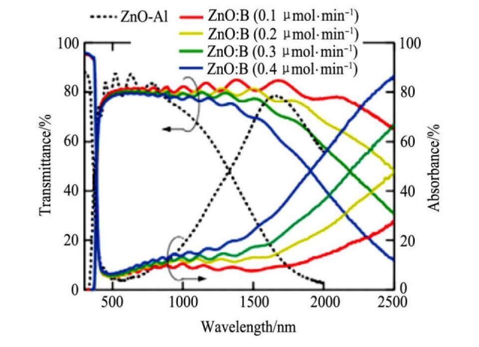
��CdS��ı�������Ҫ����һ��߶����ġ����к��ʴ�϶(>3.3 eV)��n��������������(TCO)��䵱ǰ�Ӵ�,Ҳ��Ϊ���ڲ�,���������ǽ���䵽���������������ղ���,ͬʱ��Ϊ�����ӵĴ���ͨ����CIGS������Ĵ��ڲ���˫��ZnO��:�ɱ�(100 nm)����ZnO��ͺ�(300 nm)n�Ͳ���ZnO����ɡ�����ZnO����Խ�CdS��Ͳ���ZnO�����,����ֹ����Ԫ����ɢ���������С������ӵ�ZnO(ZnO:Al,AZO)����CIGS̫���������õ����缫����,һ��ͨ���������,�����ZnO:B,ZnO:Ga���Ҳ��������TCO�㡣��AZO��Ĥ��,���ӵ�Al3+ ���Zn2+ ���ڱ�Ĥ�в������������������,���,AZO��Ĥ��ZnO��Ĥ���и��͵ĵ�����
[64 ]
���������ʹ�û�ѧ������������������п(ZnO:B,BZO)��ΪTCO�㡣������CIGS���ݵij�������,��ʵ�ָߴ�40cm2 ��V-1 ��s-1 �ĸ�Ǩ����,ͬʱ�������ܶȱ�����1��1020 cm-3 ����,��������ʹTCO�����ȺͶ�·�����������,��ͼ6��ʾ
[65 ]
��������������CIGS�ĸ�Ǩ����TCO����о�����������δ����ZnO,�⻯������(IOH)��������п(IZO)��
[66 ,67 ,68 ,69 ]
��
��2 �������ӻ����(ʹ�ò�ͬ�����Ʊ�)��CIGS��ص����� ����ԭͼ
Table 2 Performance of CIGS solar cell with cadmium free buffer layer (prepared by different methods)
[55-59]
TCO���ϵ�ѡ�������䵼���ԡ����ȡ�ˮ���ȶ��Ժͽ�һ���ӹ��������Ե��������ġ�AZOĤ��Al�Ĵ�����ǿ��Ĥ����ʪ��,��ˮ�ֶ�AZO��Ĥ���к���,�ڳ�ʪ�Ļ�����,AZO��Ĥ����ִ�Լһ���������ĵ����ʵ��˻�
[69 ]
��������Ϊ�����е��������˻�ѧ����,�γ���������п��̼����
[70 ]
,���¾��紦�γ�������,������Ǩ���ʡ����,��AZO����CIGS̫�����ʱ,���ڵ���Ҫ������AZO�ij����ȶ��ԡ�Ŀǰ����ͨ�����Ӳ��ܶ�
[71 ,72 ]
��ʹ���ʵ��ķ�װ(������з���Ϳ�����ǰ��)
[73 ]
����ֹTCO��ʪ�Ȼ����еı�¶������֮��Ҳ����ѡ������TCO����,����������(ITO)��������п(IZO)������ʪ���ȶ���
[74 ,75 ]
��
ͼ6 SLG��ZnO:Al��ZnO:B��Ĥ�����ʺ����չ���
Fig.6 Transmittance and absorption spectra of ZnO:Al and ZnO:Bfilms on SLG
[65]
2.4 ����ۻ�
�о�����,���洦�������Ӹ�����Ȼ������CIGS̫����ط�չ����Ҫԭ��֮һ,���������ۻ����Ĺ۵㱻���,�Լ������ղ�����ͱ�����洦�ĸ��ϡ�
���õ�������洦���ֶγ���ǰ����˵�ļ����PDT������CdS�����CdԪ�ص���ɢ֮��,������:(1)ͨ�������ղ��������������ı����ղ�����϶���ۻ�����ȱ��,�Ӷ�����CIGS/CdS���洦�ĸ���;(2)��СCIGS�ı����
��(<50 nm),ʹCIGS/CdS����ı������С,�Լ��ٽ��洦�ĸ��ϼ����͵���,��������ƽ���ı����ʹ��������;(3)���ղ�Ľṹ�������Ӿ�Ե�ۻ���ȡ���CIGS̫����صı��Ӵ����洦,ͨ���������ղ���Ga���ݶȱ仯�����ı��泡(BSF)
[76 ]
,ʹ����������Զ��Mo/CIGS����Ӷ����ٱ�����洦�ĸ��ϡ�
����֮��,������ʹ�������ھֲ���Ӵ��Ķۻ�����
[77 ]
�����ַ�����һ�ֽӽ�Ӧ���ڸ�Ч�ʹ��̫������ϵĶۻ�����
[78 ]
���÷��������ղ�����ͱ��涼����Ӧ��,�����������Ƶ������,�����Ƕ��ڷdz����Ļ��Ga�ݶȱ仯��CIGS���ղ�,��Ϊ����е�����Ga�ݶȲ����Է�ֹ���Ӵ��������������Ӹ��ϡ�������(Al2 O3 )�Ǿ�����������Ӧ�õIJ���֮һ,�����Լ��ٷǷ��临��,��ALD���Ʊ���AI2 O3 ��ĿǰCIGS����нϳ��õĶۻ�����
[79 ,80 ]
��
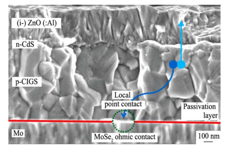
Vermang��
[81 ]
ʹ��̫�����ģ������(SCAPS)���е�ģ�����,������Ӵ�����Al2 O3 �ۻ��������ղ�ֲ���Ӵ�,CIGS�����ı��渴���ٶȿ��Դ�1��104 ��1��106 cm-1 ����1��102 ��1��103 cm-1 ��ͨ�����ʵ��,��ͼ7��ʾ,Vermang��
[82 ]
��֤��ʹ��5 nm��ALD-Al2 O3 �ۻ�CIGS�����,��ʹ��CdS����
[77 ]
����������
[73 ]
��CBD-CdS�в�����Ӵ��Ŀ���,�����ۻ��õ������Ľ�,Voc ��������,�ر��Ƕ��ڱ�(<1.6��m����Ga�ݶȱ仯���ղ��Ч���������Ľ�,��Ϊ�����ֻ�ĺ������ӽ���ص����Ծ���������ֱ��Ӵ��ۻ�������Ga�ݶȱ仯��������Ч��������δ���������ۻ����Ӵ�����һ��Ӱ���ǿ��Խ��и��õĹ����,�����Ѿ��в�ͬ���о����������˷����Ա��������Ч�������ԸĽ�
[83 ,84 ]
��
ͼ7 ʹ��ALD-Al2O3�ۻ�CIGS�����ʾ��ͼ
Fig.7 Schematic diagram of passivation ofrear surface of CIGS using ALD-Al2 O3
[82]
����Ӵ��ۻ������ڱ���ĵ�Ӵ��ķ�ʽ������ģ����ʾ,ͨ��ѡ����ʵĵ㿪�ڼ�����״
[85 ,86 ,87 ]
���ʵ��Ķۻ�����,������ܿ��Եõ��Ľ������ڵ�ǰ��CIGS������,��ѵ�Ӵ����Ⱥͼ�������10��100 nm��Χ��
[86 ]
��Hsu��
[80 ]
�״�ͨ��ALD����CIGS�����Ʊ�Al2 O3 ���ڽ���ۻ���ʵ�������ʹ��Ƚ�Ϊ5 nm,�Ϳ��Թ۲쵽Al2 O3 �Ķۻ�Ч����ALD-Al2 O3 �Ķۻ�Ч����Ҫ������CIGS/Al2 O3 ����ĵͽ���ȱ���ܶȺͿ�״Al2 O3 �еĴ�����Ĺ̶���ɲ����ij�ЧӦ������
����,ZnS��Ҳ������Ϊһ����Ч�ضۻ���
[88 ]
��ʵ��֤��In2 S3 ������CIGS���ղ�֮���ZnS���������̫����ص�����,�����Voc
[89 ]
,ZnS�ۻ���(������ILGAR��������ZnS�������Ʊ�)�뻺����Ӵ���̫������Ѿ����Ʊ�����
[90 ]
,���������ᄃ�������ղ�����ϵ�����װ,���������ۻ��������ģ��
[91 ]
��
3 CIGS��ز�ҵ�����ٵ���ս
(1)���Ч�ʡ�
������CIGS��صļ���Ч��Ϊ33.5%(��Ӧ��϶1.14 eV)
[30 ]
,����ǰ��ʵ����Ч��ˮƽ��߽�Ϊ22.9%����,���������ĵ��Ч�ʸ���,����δ�����Ƶļ��������ڷ��ƻ�����������CIGS��Ĥ�ĺ�Ⱥͳɷ֡�ʵ����Ч��(22.9%)
[12 ]
����ҵģ��Ч��(16.1%)
[92 ]
֮����ڽϴ��ࡣCIGS��ҵ������Ҫ��ս�ǽ�ʵ���ҵ����켼����չ����ģ����ҵ������,ͬʱ���ָ�Ч�ʡ����ڸ�Ч��CIGS���,ʵ�����о����õ��Ǿ�̬��������(�ĵ״��ڹ̶�λ��)������������������,���������̫�����һ����ö�̬��������(�ĵ����˶���),�����ֹ��յ���������ѧ�Dz�ͬ��
[30 ]
�������豸����������,�ڴ�����Ϻ�������С�����صĸ�Ч�ʡ����������Ҫ�Ľ��ؼ��豸����Ӧȫ��̬�������Ʊ�,ͬʱ����ص���������ѧ���н�һ���о���
(2)�������ա�
CIGS��һ����Ԫ������,������ĵ��ϵı�Ĥ������(��Ⱥͳɷ�)�Ե�ص����������˵��һ����Ҫ���⡣��Ĥ�����ԶԸ�Ч��̫����صĵ�ѧ��ѧ����Ӱ��ܴ�,ͬʱ�������Ĥ���ظ��Ժ;�����ֱ��Ӱ���Ʒ�������Ͳ��������CIGS̫����ص������漰����պ�������ֹ���(����CBD�Ʊ�CdS,��ռ����Ʊ�CIGS),��ͬ�豸֮��Ļ��崦������֮���ͨ�����춼�������ϵĹؼ�����
[93 ]
����һ��Ŀǰ����ͨ��ʹ����չ����Ʊ����б�Ĥ������,����ý����������,��������������ɱ���
(3)�����װ��
�ڵ���ȶ��Է���,Ŀǰ������о�������δ��װ��CIGS����Ͻ��е�
[87 ]
��Theelen��
[94 ]
���о�����,���缫���Ľ��淴Ӧ�Ե����˵������Ҫ,��Mo���缫���ں����������ͽ���,�ᵼ�µ������IJ��ȶ���Ϊ�����CIGS̫����صij����ȶ���,��Ҫһ�ָ����ȶ��ı��Ӵ���ͬʱ����TCO��Ĥ��ˮ�ֺͿ����б�¶Ҳ���������ܵ��˻�
[64 ]
,���Ի���ZnO��Mo�ĸ�ʴ��,ʹ����ϩ-������ϩ������(EVA)/������CIGS��������ںܴ�����⡣Ϊ�˱���ʪ������������,CIGS�����Ҫһ�־��и�������(��ճ����,�;���,��ʪ�ʺ����ȶ��Ե�)�ĺ��ʵ��ܷ⼼����
(4)ԭ�����������ɱ���
�����ӱ������ж���,��Ի�����������Ӱ��,�������������������
[88 ]
,���Զ����ӵ�CIGS��ص��о��dz���Ҫ������,In�ڹ�ҵ��������Ҫ����ΪZn�ĸ���Ʒ��õ�,�����������Zn����������
[95 ]
������Ԥ��,In�������������CIGS����Ĵ�������������,��ᵼ����۸�������ͬʱGaԪ���ڵ����ϴ��������ḻ,��۸��Ϊ����Ϊ�˽���������,��Ҫ������ղ�Ĺ�������������,ͨ�����ϵ��Ż����������ṹ������,ʹ��������CIGS�����(��1��m),ͬʱ����Jsc ����ʧ��Ϊ���������ɱ�,Ӧ����CIGS��TCO����Ʊ�ʱ��,����Ҳ��Ҫʹ�ø�����CIGS�㲢�Ҳ���TCO�ĸ�������������
4 չ��
������,CIGS̫����ص��о�ȡ������Ҫ��չ,�ɲ�ͬʵ���Ҵ���������¼Ч�ʷ�������,���ǵ�ǰ��¼Ч��������Ч��ֵ�����ڽϴ��ࡣ�¼����ij���������CIGS���Ч�ʵļ�����,������Щ�����Ļ�����֪������Ч�ʵĹؼ����¼�������CIGS̫����������Ի����ϵ�����,CIGS����ѿ��صĵ���Ȳ���,�Ѿ���Ϊ���µķ�չ����Ŀǰʵ�����о��ɹ�Ӧ�������������ʹ��Ͳ�ҵ����������ս,ʵ�����о�����ת��Ϊ��ҵ��������Ҳ��Ҫһ��ʱ�䡣����,��CIGS��ص��о�Ҳ��Ҫ��һ���,�Ӹ�Դ�������Ƶ�����ܡ�
�����
[1] Jackson P,Wuerz R,Hariskos D,Lotter E,Witte W,Powalla M.Effects of heavy alkali elements in Cu(In,Ga)Se_2 solar cells with efficiencies up to 22.6%[J].Physica Status Solidi(RRL)-Rapid Research Letters,2016,10(8):583.
[2] Jeyakumar R,Ramamurthy S,Jayachan-dran M,Chockalingam M J.Electrochemical preparation and characterization of copper indium diselenide thin films[J].Materials Research Bulletin,1994,29(2):195.
[3] Hahn H,Frank G,Klingler W,Anne D S,Georg S.Untersuchungen��bertem?re Chalkogenide.V.Ubereinigetem?re chalkogenidemit chalkopyritstruktur[J].Zeitschrift f��r Anorganische und Allgemeine Chemie,1953,271:153.
[4] Wagner S,Shay J L,Migliorato P,Piero M,Kasper H M.CuInSe_2/CdS heterojunction photovoltaic detectors[J].Applied Physics Letters,1974,25(8):434.
[5] Kazmerski L L,White F R,Morgan G K.Thin-film CuInSe_2/CdS heterojunction solar cells[J].Appl.Phys.Lett.,1976,29:268.
[6] Boer K W.Solar Cell Theory[M].Physics and Technology of Solar Energy.Springer Netherlands,1987.9.
[7] Kazmerski L L,Sanborn G A.CuInS_2 thin-film homojunction solar cells[J].Journal of Applied Physics,1977,48(7):3178.
[8] Mickelsen R A,Chen W S.Development of a 9.4%efficient thin-film CuInSe_2/CdS solar cell[A].15th Photovoltaic Specialists Conference[C].1981.800.
[9] Mitchell K,Eberspacher C,Ermer J,Pier D.Single and tandem junction CuInSe_2,cell and module technology[A].Photovoltaic Specialists Conference,1988.Conference Record of the Twentieth IEEE[C].IEEE,1988.1384.
[10] Wieting R D.CIS manufacturing at the megawatt scale[A].Photovoltaic Specialists Conference,2002.Conference Record of the Twenty-Ninth IEEE[C].IEEE,2002.478.
[11] Rui K,Yagioka T,Adachi S,Handa A,Tai K F,Takuya K,Hiroki S.New world record Cu(In,Ga)(Se,S)2 thin film solar cell efficiency beyond 22%[A].Photovoltaic Specialists Conference[C].IEEE,2016.1287.
[12] Green M,Hishikawa Y,Dunlop E,Dean H L,Jochen H E,Anita H B.Solar cell efficiency tables(version51)[J].Progress in Photovoltaics Research&Applications,2018,26(1):51.
[13] Reinhard P,Pianezzi F,Bissig B,Chirila A,Blosch P,Nishiwaki S,Buecheler S,Tiwari A N.Cu(In,Ga)Se_2thin-film solar cells and modules��a boost in efficiency due to potassium[J].IEEE Journal of Photovoltaics,2015,5(2):656.
[14] Rampino S,Annani N,Bissoli F,Rampino S,Annani N,Bissoli F,Bronzoni M,Calestani D,Calicchio M.15%efficient Cu(In,Ga)Se_2 solar cells obtained by lowtemperature pulsed electron deposition[J].Applied Physics Letters,2012,101(13):894.
[15] Fischer J,Larsen J K,Guillot J,Aidac Y,Eisenbartha T,Regescha D,Depreduranda V,Fevrea N,Siebentritta S,Phillip J D.Composition dependent characterization of copper indium diselenide thin film solar cells synthesized from electrodeposited binary selenide precursor stacks[J].Solar Energy Materials&Solar Cells,2014,126(126):88.
[16] Kapur V,Kemmerle R,Bansal A,Haber J,Schmitzberger J,Le P,Guevarra D,Kapur V,StempienT.Manufacturing of ��ink based�� CIGS solar cells/modules[A].Photovoltaic Specialists Conference,2008.Pvsc'08[C].IEEE,2009.1.
[17] Nakada T.Invited paper:CIGS-based thin film solar cells and modules:unique material properties[J].Electronic Materials Letters,2012,8(2):179.
[18] Romeo A,Terheggen M,Abou-Ras D,B?tzner D L,Haug F J,Kalin M,Rudmann D,Tiwari A N.Development of thin-film Cu(In,Ga)Se_2 and CdTe solar cells[J].Progress in Photovoltaics Research&Applications,2004,12(2-3):93.
[19] Guillemoles J F.The puzzle of Cu(In,Ga)Se_2,(CIGS)solar cells stability[J].Thin Solid Films,2002,s 403-404(-):405.
[20] Kannan R,Miguel A,Contreras,Craig L.Perkins.Properties of 19.2%efficiency ZnO/CdS/CuInGaSe2thin-film solar cells[J].Progress in Photovoltaics Research&Applications,2010,11(4):225.
[21] Katagiri H.Survey of development of CZTS-based thin film solar cells[A].IEEE,International Conference on Photonics[C].IEEE,2012.345.
[22] Ghorbani E,Kiss J,Mirhosseini H,Roma G,Schmidt M,Windeln J,K��hne T D,Felser C.Hybridfunctional calculations on the incorporation of Na and K impurities into the CuInSe_2 and CuIn_5Se_8 solar-cell materials[J].Journal of Physical Chemistiy C,2015,119(7):151014100345001.
[23] Reinhard P,Chirila A,Blosch P,Pianezzi F,Nishiwaki S,Buecheler S,Tiwari A N.Review of progress toward20%efficiency flexible CIGS solar cells and manufacturing issues of solar modules[J].IEEE Journal of Photovoltaics 2013,3(1):572.
[24] Shafarman W N,Stolt L.Cu(InGa)Se_2 Solar Cells[M].Handbook of Photovoltaic Science and Engineering.John Wiley&Sons,Ltd.,2010.546.
[25] Scheer R,Schock H W.Chalcogenide Photovoltaics:Physics,Technologies,and Fhin Film Devices[M].Wiley-VCH,2011.159.
[26] Fortunato E,Ginley D,Hosono H,Paine D C.Transparent conducting oxides for photovoltaics[J].Mrs Bulletin,2007,32(3):242.
[27] Rau U,Grabitz P 0,Werner J J H.Resistive limitations to spatially inhomogeneous electronic losses in solar cells[J].Applied Physics Letters,2004,85(24):6010.
[28] Naghavi N,Abou-Ras D,Allsop N,Barreau N,B��cheler S,Ennaoui A,Fischer C H,Guillen C,Hariskos D,Herrero J,Klenk R,Kushiya K,Lincot D,Menner R,Nakada T,Platzer-Bj?rkman C,Spiering S,Tiwari A N,T?mdahl T.Buffer layers and transparent conducting oxides for chalcopyrite Cu(In,Ga)(S,Se)_2,based thin film photovoltaics:present status and current developments[J].Progress in Photovoltaics Research&Applications,2010,18(6):411.
[29] Ramanujam J,Venna A,Gonzalez-Diaz B,GuerreroLemus R,Cirlin G E.Inorganic photovoltaics-Planar and nanostructured devices[J].Progress in Materials Science,2016,82:294.
[30] Ramanujam J,Singh U P.Copper indium gallium selenide based solar cells-a review[J].Energy&Environmental Science,2017.
[31] Hedstrom J,Ohlsen H,Bodegard M,Kylner A,Stolt L,Hariskos D,Ruckh M,Schock H W.ZnO/CdS/Cu(In,Ga)Se_2 thin film solar cells with improved performance[A].Photovoltaic Specialists Conference,1993.Conference Record of the Twenty Third IEEE[C].IEEE Xplore,1993.364.
[32] Rudmann D,Bremaud D,Cunha A F D,Bilger G,Strohm A,Kaelin M,Zogg H,Tiwari A N.Sodium incorporation strategies for CIGS growth at different temperatures[J].Thin Solid Films,2005,480(11):55.
[33] Jackson P,Hariskos D,Lotter E,Paetel S,Wuerz R,Menner R,Wischmann W,Powalla M.New world record efficiency for Cu(In,Ga)Se_2 thin-film solar cells beyond 20%[J].Progress in Photovoltaics Research&Applications,2011,19(7):894.
[34] Chirila A,Reinhard P,Pianezzi F,Bloesch P,Alexander R Uhl,Fella C,Kranz L,Keller D,Gretener C,Hagendorfer H,Jaeger D,Emi Rolf,Nishiwaki S,Buecheler S,Tiwari A N.Potassium-induced surface modification of Cu(In,Ga)Se_2 thin films for high-efficiency solar cells[J].Nature Materials,2013,12(12):1107.
[35] Green M A,Emery K,Hishikawa Y,Warta W,Dunlop E D.Solar cell efficiency tables(version 41)[J].Progress in Photovoltaics Research&Applications,2013,21(1):49.
[36] Jackson P,Hariskos D,Wuerz R,Wischmann W,Powalla M.Compositional investigation of potassium doped Cu(In,Ga)Se_2,solar cells with efficiencies up to 20.8%[J].Physica Status Solidi(RRL)-Rapid Research Letters,2014,8(3):219.
[37] Jackson P,Hariskos D,Wuerz R,Kiowski O,Bauer A,Friedlmeier T M,Powalla M.Properties of Cu(In,Ga)Se_2 solar cells with new record efficiencies up to 21.7%[J].Physica Status Solidi(RRL)-Rapid Research Letters,2015,9(1):28.
[38] Theresa M F,Philip J,Andreas B,Dimitrios H,Oliver K,Richard M,Roland W,Michael P.High-efficiency Cu(In,Ga)Se_2 solar cells[J].Thin Solid Films,2017,633:13.
[39] Jackson P,Wuerz R,Hariskos D,Lotter E,Witte W,Powalla M.Effects of heavy alkali elements in Cu(In,Ga)Se_2 solar cells with efficiencies up to 22.6%[J].Physica Status Solidi(RRL)-Rapid Research Letters,2016,10(8):583.
[40] Paetel S.Roadmap CIGS towards 25%efficiency[presentation][R].7th International Workshop on CIGS Solar Cell Technology[C].Munich,Gennany,2016.
[41] Yun S,Shuping L,Li Wei,Shiqing C,Yunxiang Z,Yiming L,Wei L.Review on alkali element doping in Cu(In,Ga)Se_2 thin films and solar cells[J].Engineering,2017,3(4):452.
[42] Pianezzi F,Reinhard P,Chirila A,Bissig B,Nishiwaki S,Buecheler S,Tiwari A N.Unveiling the effects of post-deposition treatment with different alkaline elements on the electronic properties of CIGS thin film solar cells[J].Physical Chemistry Chemical Physics Peep,2014,16(19):8843.
[43] Handick E,Reinhard P,Alsmeier J H,Kohler L,Pianezzi F,Krause S,Gorgoi M,Ikenaga E,Koch N,Wilks R G,Buecheler S,Tiwari A N,B?r M.Potassium postdeposition treatment-induced band gap widening at Cu(In,Ga)Se_2 surfaces-reason for performance leap[J].Acs Applied Materials&Interfaces,2015,7(49):27414.
[44] Mahboob S,Malik S N,Haider N,Nguyen C Q,Malik M A,O'Brien P.Deposition of binary,ternary and quaternary metal selenide thin films from diisopropyldiselenophosphinato-metal precursors[J].Journal of Crystal Growth,2014,394(10):39.
[45] Xiao H,Tahirkheli J,Iii W A G.Accurate band gaps for semiconductors from density functional theory[J].2011,2(3):212.
[46] Witte W,Abou-Ras D,Albe K,Bauer G H,Bertram F,Boit C,Br��ggemann R,Christen J,Dietrich J,Eicke A,Hariskos D,Maiberg M,Mainz R,Meessen M,M��ller M,Neumann O,Orgis T,Paetel S,Pohl J,Rodriguez-Alvarez H,Scheer R,Schock H W,Unold T,Weber A,Powalla M.Gallium gradients in Cu(In,Ga)Se_2 thin-film solar cells:gallium gradients in CIGS thin-film solar cells[J].Progress in Photovoltaics Research&Applications,2015,23:717.
[47] Schleussner S,Zimmennann U,W?tjen T,Leifer K,Edoff M.Effect of gallium grading in Cu(In,Ga)Se_2,solar-cell absorbers produced by multi-stage coevaporation[J].Solar Energy Materials&Solar Cells,2011,95(2):721.
[48] Chirila A,Buecheler S,Pianezzi F,Bloesch P.Gretener C,Uhl A R,Fella C,Kranz L,Perrenoud J,Seyrling S,Venna R,Nishiwaki S,Romanyuk Y E,Bilger G,Tiwari A N.Highly efficient Cu(In,Ga)Se_2solar cells grown on flexible polymer films[J].Nature Materials,2011,10(11):857.
[49] Dullweber T,Hanna G,Shams-Kolahi W,Schwartzlander A,Contreras M A,Noufi R,Schock H W.Study of the effect of gallium grading in Cu(In,Ga)Se_2[J].Thin Solid Films,2000,s361-362(7):478.
[50] Gorji N E,Reggiani U,Sandrolini L.A simple model for the photocurrent density of a graded band gap CIGS thin film solar cell[J].Solar Energy,2012,86(3):920.
[51] Dullweber T,Anna G H,Rau U,Schock H W.A new approach to high-efficiency solar cells by band gap grading in Cu(In,Ga)Se_2 chalcopyrite semiconductors[J].Solar Energy Materials&Solar Cells,2001,67(1):145.
[52] Amin N,Chelvanathan P,Hossain M I,Sopian K.Numerical modelling of ultra thin Cu(In,Ga)Se_2 solar cells[J].Energy Procedia,2012,15(1):291.
[53] Wada T,Hayashi S,Hashimoto Y,Nishiwaki S,Sato T,Negami T,Nishitani M.High efficiency Cu(In,Ga)Se_2(CIGS)solar cells with improved CIGS surface[A].Proceedings of the 2nd World Conference and Exhibition on Photovoltaic Energy Conversion[C].1998.403.
[54] Fjallstrom V,Szaniawski P,Vennang B,Salome P M P,Rostvall F,Zimmennann U,Edoff M.Recovery after potential-induced degradation of Culn_(1-x)Ga_xSe_2 solarcells with CdS and Zn(O,S)buffer layers[J].2015,5(2):664.
[55] Nakamura M,Kouji Y,Chiba Y,Hakuma H,Kobayashi T,Nakada T.Achievement of 19.7%efficiency with a small-sized Cu(InGa)(SeS)_2 solar cells prepared by sulfurization after selenizaion process with Zn-based buffer[A].IEEE Photovoltaic Specialists Conference[C].IEEE,2013.0849.
[56] Kobayashi T,Yamaguchi H,Nakada T.Effects of combined heat and light soaking on device performance of Cu(In,Ga)Se_2,solar cells with ZnS(O,OH)buffer layer[J].Progress in Photovoltaics Research&Applications,2014,22(1):115.
[57] Hariskos D,Menner R,Jackson P,Paetel S,Witte W,Wischmann W,Powalla M,B��rkert L,Kolb T,Oertel M,Dimmler B,Fuchs B.New reaction kinetics for a high-rate chemical bath deposition of the Zn(S,O)buffer layer for Cu(In,Ga)Se_2-based solar cells[J].Progress in Photovoltaics Research&Applications,2012,20(5):534.
[58] Naghavi N,Abou-Ras D,Allsop N,Barreau N,B��cheler S,Ennaoui A,Fischer C H,Guillen C,Hariskos D,Herrero J,Klenk R,Kushiya K,Lincot D,Menner R,Nakada T,Platzer-Bj?rkman C,Spiering S,Tiwari A N,T?rndahl T.Buffer layers and tmnsparent conducting oxides for chalcopyrite Cu(In,Ga)(S,Se)_2based thin film photovoltaics:present status and current developments[J].Progress in Photovoltaics Research&Applications,2010,18(6):411.
[59] Salome P M P,Keller J,Tomdahl T,Teixeira J P,Nicoara N,Andrade R R,Stroppa D G,Gonzalez J C,Edoff M,Leitao J P,Sadewasser S.CdS and Zn_(1-x)Sn_xO_y,buffer layers for CIGS solar cells[J].Solar Energy Materials&Solar Cells,2017,159:272.
[60] Meyer B K,Polity A,Farangis B,He Y,Hasselkamp D,Kr?mer Th,Wang C.Structural properties and bandgap bowing of ZnO_(1-x)S_x thin films deposited by reactive sputtering[J].Applied Physics Letters,2004,85(21):4929.
[61] Persson C,Platzer-Bj?rkman C,Malmstr?m J,Tomdahl T,Edoff M.Strong valence-band offset bowing of ZnO_(1-x)S_x,enhances p-type nitrogen doping of ZnO-like alloys[J].Physical Review Letters,2006,97(14):146403.
[62] Grimm A,Kieven D,Klenk R,Lauennann I,NeisserA,Niesen T,Palm J.Junction formation in chalcopyrite solar cells by sputtered wide gap compound semiconductors[J].Thin Solid Filins,2011,520(4):1330.
[63] Spiering S,Nowitzki A,Kessler F,Igalson M,Maksoud H A.Optimization of buffer-window layer system for CIGS thin film devices with indium sulphide buffer by inline evaporation[J].Solar Energy Materials&Solar Cells,2016,144:544.
[64] Pan J,Kerr L,Li X,Gulley-Stahl H J,Sommer A J.Investigation of aluminum induced degradation in sputtered Al:ZnO for CIGS solar cells applications[A].In:IEEE Photovoltaic Specialists Conference[C].IEEE,2009.000345.
[65] Koida T,Nishinaga J,Higuchi H,Kurokawa A,Iioka M,Kamikawa-Shimizu Y,Yamada A,Shibata H,Niki S.Comparison of ZnO:B and ZnO:Al layers for Cu(In,Ga)Se_2 submodules[J].Thin Solid Filins,2016,4(4):79.
[66] Hala M,Fujii S,Redinger A,Inoue Y,Rey G,Thevenin M,Depredurand V,Weiss T P,Bertram T,Siebentritt S.Highly conductive ZnO films with high near infrared transparency[J].Progress in Photovoltaics Research&Applications,2015,23(11):1630.
[67] Koida T,Fujiwara H,Kondo M.Hydrogen-doped In_2O_3 as high-mobility transparent conductive oxide[J].Japanese Journal of Applied Physics,2007,46(25-28):L685.
[68] Menner R,Cemernjak M,Paetel S,Wischmann W.Application of indium zinc oxide window layers in Cu(In,Ga)Se_2,solar cells[J].Thin Solid Films,2016.
[69] Jager T,Romanyuk Y E,Nishiwaki S,Benjamin B,Fabian P,Peter F,Christina G,Max D,Tiwair A N.Hydrogenated indium oxide window layers for highefficiency Cu(In,Ga)Se_2 solar cells[J].Journal of Applied Physics,2015,117(20):28.
[70] Theelen M,Boumans T,Stegeman F,Colberts F,Illiberi A,Berkum J,Barreau N,Vroon Z,Zeman M.Physical and chemical degradation behavior of sputtered aluminum doped zinc oxide layers for Cu(In,Ga)Se_2,solar cells[J].Thin Solid Films,2014,550(550):530.
[71] Hiipkes J,Owen J I,Wimmer M,Ruske F,Greiner D,Klenk R,Zastrow U,Hotovy J.Damp heat stable doped zinc oxide films[J].Thin Solid Filins,2014,555(555):48.
[72] Greiner D,Gledhill S E,Koble C,Krammer J,Klenk R.Damp heat stability of Al-doped zinc oxide films on smooth and rough substrates[J].Thin Solid Films,2011,520(4):1285.
[73] Carcia P F,Mclean R S,Hegedus S.Encapsulation of Cu(InGa)Se_2 solar cell with Al_2O_3 thin-film moisture barrier grown by atomic layer deposition[J].Solar Energy Materials&Solar Cells,2010,94(12):2375.
[74] Pem F J,Noufi R,Li X,Dehart C,To B.Damp-heat induced degradation of transparent conducting oxides for thin-film solar cells[A].Photovoltaic Specialists Conference,2008.Pvsc'08.IEEE[C].IEEE,2008.1.
[75] Coyle D J,Blaydes H A,Northey R S,Pickett J E,Nagarkar K R,Zhao R A,Gardner J 0.Life prediction for CIGS solar modules part 2:degradation kinetics,accelerated testing,and encapsulant effects[J].Progress in Photovoltaics Research&Applications,2013,21(2):173.
[76] Lundberg O,Edoff M,Stolt L.The effect of Gagrading in CIGS thin film solar cells[J].Thin Solid Films,2005,480(3):520.
[77] Vennang B,Fjallstrom V,Pettersson J,Salome P,Edoff M.Development of rear surface passivated Cu(In,Ga)Se_2,thin film solar cells with nano-sized local rear point contacts[J].Solar Energy Materials&Solar Cells,2013,117(4):505.
[78] Blakers A W,Wang A,Milne A M,Zhao J,Green M A.22.8%efficient silicon solar cell[J].Applied Physics Letters,1989,55(13):1363.
[79] Joel J,Vennang B,Larsen J,Donzel-Gargand O,Edoff M.On the assessment of CIGS surface passivation by photoluminescence[J].Physica Status Solidi(RRL)-Rapid Research Letters,2015,9(5):288.
[80] Hsu W W,Chen J Y,Cheng T H,Lu S C,Ho W S,Chen Y Y,Chien Y J,Liu C W.Surface passivation of Cu(In,Ga)Se_2 using atomic layer deposited Al_2O_3[J].Applied Physics Letters,2012,100(2):235.
[81] Vennang B,W?tjen J T,Frisk C,Fj?llstr?m V,Rostvall F,Edoff M,Salome P,Bonne J,Nicoara N,Sadewasser S.Introduction of Si PERC rear contacting design to boost efficiency of Cu(In,Ga)Se solar cells[J].Photovoltaics IEEE Journal of Photovoltaics,2014,4(6):1644.
[82] Vennang B,Fj?llstr?m V,Gao X,Edoff M.Improvedrear surface passivation of Cu(In,Ga)Se,solar cells:a combination of an Al,O,rear surface passivation layer and banosized local rear point contacts[J].IEEE Journal of Photovoltaics,2014,4(1):486.
[83] Vermang B,W?tjen J T,Fj?llstr?m V,Rostvall F,Edoff M,Gunnarsson R,Pilch I,Helmersson U,Kotipalli R,Henry F,Flandre D.Highly reflective rear surface passivation design for ultra-thin Cu(In,Ga)Se_2solar cells[J].Thin Solid Films,2015,582:300.
[84] Van L C,Yin G,Polman A,Schmid M.Light coupling and trapping in ultrathin Cu(In,Ga)Se_2 solar cells using dielectric scattering patterns[J].Acs Nano,2015,9(10):9603.
[85] Sozzi G,Pignoloni D,Menozzi R,Pianezzi F,Reinhard P,Bissig B,Buecheler S,Tiwari A N.Designing CIGS solar cells with front-side point contacts[A].Photovoltaic Specialist Conference[C].IEEE,2015.1.
[86] Bercegol A,Chacko B,Klenk R,LauennannI,LuxSteiner M C,Liero M.Point contacts at the copper-indium-gallium-selenide interface��a theoretical outlook[J].Journal of Applied Physics,2016,119(15):1107.
[87] Allsop N,N��mberg R,Lux-Steiner M C,SchedelNiedrig T.Three-dimensional simulations of a thin film heterojunction solar cell with a point contact/defect passivation structure at the heterointerface[J].Applied Physics Letters,2009,95(12):235.
[88] Hultqvist A,Li J V,Kuciauskas D,Dippo P,Contreras M A,Levi D H,Bent S F.Reducing interface recombination for Cu(In,Ga)Se_2 by atomic layer deposited buffer layers[J].Applied Physics Letters,2015,107(3):28.
[89] Allsop N A,Camus C,H?nsel A,Gledhilll S E,Lauernann I,Lux-Steiner M C,Fischer C H.Indium sulfide buffer/CIGSSe interface engineering:Improved cell performance by the addition of zinc sulfide[J].Thin Solid Films,2007,515(15):6068.
[90] Fu Y,Saez-Araoz R,Kohler T,Kr��ger M,Steigert A,Lauennann I,Lux-Steiner M C,Fischer C H.SprayILGAR ZnS nanodots/In_2S_3,as defect passivation/point contact bilayer buffer for Cu(In,Ga)(S,Se)_2,solar cells[J].Solar Energy Materials&Solar Cells,2013,117(10):293.
[91] Reinhard P,Bissig B,Pianezzi F,Hagendorfer H,Sozzi G,Menozzi R,Gretener C,Nishiwaki S,Buecheler S,Tiwari A N.Alkali-templated surface nanopatteming of chalcogenide thin films:a novel approach towards solar cells with enhanced efficiency[J].Nano Letters,2015,15(5):3334.
[92] Green M A.Estimates of Te and In prices from direct mining of known ores[J].Progress in Photovoltaics Research&Applications,2009,17(5):347.
[93] Theelena M,Daume F.Stability of Cu(In,Ga)Se_2solar cells:a literature review[J].Sol.Energy,2016,133:586.
[94] Theelen M,Polman K,Tomassini M,Barreau N,Steijvers H,Berkum J,Vroon Z,Zeman M.Influence of deposition pressure and selenisation on damp heat degra-dation of the Cu(In,Ga)Se_2,back contact molybdenum [J].Surface&Coatings Technology,2014,252(9):157.
[95] Ramanujam J,Venna A,Gonzalez-Diaz B,Guerrero-Le-musd R,Canizo C,Garcia-Tabares E,Rey-Stolle I,Granek F,Korte L,Tucci M,Rath J,Singh U P,Todorov T,Gunawan 0,Rubio S,Plaza J L,Dieguez E,Hoffmann B,Cirlin G E.Inorganic photovoltaics-Planar and nanostructured devices[J].Progress in Ma-terials Science,2016,82:294.