
J. Cent. South Univ. Technol. (2010) 17: 1163-1171
DOI: 10.1007/s11771-010-0613-2![]()
Structural evolution and optical characterization in argon diluted Si:H thin films obtained by plasma enhanced chemical vapor deposition
LI Zhi(��־)1, HE Jian(�ν�)1, LI Wei(��ΰ)2,
CAI Hai-hong(�̺���)1, GONG Yu-guang(�����)1, JIANG Ya-dong(���Ƕ�)2
1. School of Optoelectronic Information, University of Electronic Science and Technology of China,
Chengdu 610054, China;
2. State Key Laboratory of Electronic Thin Films and Integrated Devices,
University of Electronic Science and Technology of China, Chengdu 610054, China
? Central South University Press and Springer-Verlag Berlin Heidelberg 2010
Abstract:
The structural evolution and optical characterization of hydrogenated silicon (Si:H) thin films obtained by conventional radio frequency (RF) plasma enhanced chemical vapor deposition (PECVD) through decomposition of silane diluted with argon were studied by X-ray diffractometry (XRD), Fourier transform infrared (FTIR) spectroscopy, Raman spectroscopy, transmission electron microscopy (TEM), and ultraviolet and visible (UV-vis) spectroscopy, respectively. The influence of argon dilution on the optical properties of the thin films was also studied. It is found that argon as dilution gas plays a significant role in the growth of nano-crystal grains and amorphous network in Si:H thin films. The structural evolution of the thin films with different argon dilution ratios is observed and it is suggested that argon plasma leads to the nanocrystallization in the thin films during the deposition process. The nanocrystallization initiating at a relatively low dilution ratio is also observed. With the increase of argon portion in the mixed precursor gases, nano-crystal grains in the thin films evolve regularly. The structural evolution is explained by a proposed model based on the energy exchange between the argon plasma constituted with Ar* and Ar+ radicals and the growth regions of the thin films. It is observed that both the absorption of UV-vis light and the optical gap decrease with the increase of dilution ratio.
Key words:
nanocrystallization; plasma enhanced chemical vapor deposition (PECVD); hydrogenated silicon (Si:H)��
1 Introduction
Hydrogenated amorphous silicon (a-Si:H) thin film has attracted considerable attention and been a subject of extensive studies worldwide on account of its important applications such as thin film solar cells, thin film transistors, radiation detectors, and liquid crystal displays based on its good electrical and optical properties [1]. However, light-induced degradation, also named Staebler- Wronski effect [2], has been a major bottleneck since it was observed in practical device applications. Due to the difficulty of this technique, several approaches aiming at eliminating it have been proposed. It has been reported that high dilution of silane (SiH4) with argon, hydrogen or helium, mixed in the high vacuum chamber of radio frequency plasma enhanced chemical vapor deposition (PECVD) system, improves stability and properties of a-Si:H thin films through partial nanocrystallization of the thin films [3-5]. So, researching on transformation of Si:H thin films from amorphous state to nanocrystalline state is prospective. Until now, the preparation of nano-crystal Si:H (nc-Si:H) and micro-crystal Si:H (?c-Si:H) thin films under high gas dilution of silane at certain RF power density has been accomplished [6-8]. But the conventional technique for crystallization using PECVD method depends extremely on high gas dilution ratio, high substrate temperature, and high RF power density [9-10]. And it has been reported that using these specified deposition parameters is always associated with undesirable disadvantages like low deposition speed and unavoidable etching effect [11], which reduces the deposition efficiency and impairs the quality and uniformity of the thin films. Moreover, the effects of argon dilution on the crystallization process are still controversial and the existing principles of crystallization using argon dilution in RF-PECVD system are still incomplete [12-13]. Therefore, preparation of a-Si:H thin films embedded with nano-crystal grains using lower argon dilution ratio at moderate radio frequency (RF) power and discussion of phase transformation principles behind as well as the influence of the structural evolution on the optical properties of the testing films are promising and significant.
In this work, the Si:H thin films were deposited in a conventional PECVD system. By use of X-ray diffraction (XRD) spectroscopy, Fourier transform infrared (FTIR) spectroscopy, Raman spectroscopy and transmission electron microscopy (TEM), the nano-crystal grains embedded in the a-Si:H thin films were observed and the structural studies of the thin films deposited near amorphous-nanocrystalline transition region were fulfilled systematically. The optical characterization of these thin films was also appraised by ultraviolet and visible (UV-vis) spectroscopy in order to study the influence of argon dilution on the absorption of UV-vis light and the optical gap of the films. On the basis of these results, the structural evolution under low argon dilution ratio was discussed. The growth and nanocrystallization mechanisms of the thin films that involve the role of excited argon atoms in CVD plasma were also discussed under a proposed model.
2 Experimental
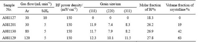
The argon diluted samples of Si:H thin films were deposited in a conventional RF (13.56 MHz) PECVD chamber, as shown in Fig.1, at gas pressure of 60 Pa, substrate temperature of 250 �� and gas temperature of 160 ��. The electrode area and the distance between the electrodes were 220 cm2 and 2 cm, respectively. Before the deposition, all substrates were cleaned strictly following a standard procedure to ensure a good adhesion between the substrate and the thin film. The mixed precursor gases were ultrahigh purity silane and argon. The dilution ratio R (the argon-to-silane flow ratio) was increased from 3 to 24 at a given RF power density of 150 mW/cm2. Raman spectroscopy researches were carried out on Si:H thin films (about 500 nm in thickness) which were deposited on K9 glass. The films (about 500 nm in thickness) for XRD and UV-vis studies were also deposited on K9 glass. FTIR analysis was accomplished on the thin films (about 500 nm in thickness) co-deposited on KBr substrate. TEM images were taken from the films (about 300 nm in thickness) deposited directly on carbon-coated copper grids, avoiding the negative influence on the thin film structure by ion milling.
In XRD analysis, conventional Cu K�� X-ray radiation (��=0.154 18 nm) was used and the measurements were taken by Philips X' Pert Pro operated at 3 kW. Further analysis of the data was accomplished using Jade5 software. To analyze bonding formation in the Si:H thin films, Bruker Tensor 27 FTIR spectroscopy apparatus was used at room temperature, and the moisture in the environment was controlled to a low level. For Raman analysis, samples were analyzed by JY HR800 at 0.1 mW, and the light resource was supplied by 532 nm laser. To observe the mixed regions in Si:H thin films, high resolution transmission electron microscopy (HRTEM) graphs were taken in an FEI Tecnai F20 field emission gun microscope. The image analysis was completed by DigitalMicrograph software. The data of optical characterization were obtained from absorption measurements in Shimadzu UV-1700 spectrophotometer.
3 Results
3.1 XRD spectroscopy
Results of XRD measurement are presented in Fig.2 for the series of samples in which nanocrystallization embedded in the a-Si:H thin films is looked forward to. The spectra for those thin films deposited under different dilution ratios R at certain RF power density are displayed. The emergence of three crystal peaks in the graph confirms the existence of crystal grains in the testing thin films under certain deposition conditions. For the patterns of XRD measurement, the peaks at different angles represent different orientations of crystal grains. The peaks observed at angles of 28.5?, 47.2? and 56.2? are assigned to Si(111), Si(220) and Si(311) reflection planes of faced-centered cubic silicon, respectively.
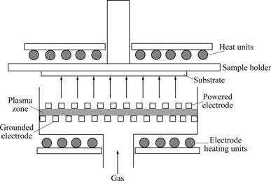
Fig.1 Sketch of PECVD device
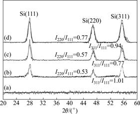
Fig.2 XRD spectra and orientation tendency of Si:H thin films deposited at 150 mW/cm2 and different R values: (a) R=3; (b) R=6; (c) R=16; (d) R=24
XRD patterns of four typical samples at the same RF power density with different dilution ratios are shown in Fig.2. At R=3 and an extremely low dilution ratio, no crystal grains are detected in this sample, indicating that there is no apparent structural evolution in the thin films. When dilution ratio R reaches 6, diffraction peaks arise. With the increase of dilution ratio, there appear three peaks symbolizing three different silicon crystalline orientations. The higher the dilution ratio R is, the sharper and higher the three peaks are. These suggest that crystal grain size and structural characteristics in the testing films evolve along with the increase of argon dilution ratio. Also, the growth of grains in the thin films is multi-oriented. Based on the widths of the XRD lines, the average grain size of different orientations in the testing thin films can be calculated using Scherrer��s equation when the grain size is in nano scale, and in this equation a decrease of grain size corresponds to an increase of peak width. The calculated data of grain size are given in Table 1.
The increase of the total intensity diffracted by the testing thin films with increasing dilution ratio suggests that the crystalline volume fraction increases accordingly. However, the exact crystalline volume fraction in each sample cannot be quantified in detail from XRD spectroscopy because of the crystallographic texture effects. Each grain embedded in the amorphous network normally has a crystallographic orientation different from that of its neighbors. Considering all grains as a whole, the orientations of each grain may be distributed randomly, or may tend to cluster around a specified preferential orientation. The grains aggregated in the latter microstructure are said to have a ��preferred orientation�� or ��texture�� which may be simply defined as a condition in which the crystal orientation is nonrandom. In our cases, the peak height ratios of I(220)/I(111) and I(311)/I(111) were used to monitor the evolution of crystallographic texture as a function of the argon dilution ratios. The data in Fig.2 show that the crystal growth in the deposition condition is random for the reason that they do not change much with the increase of dilution ratio. All of the three main orientation planes develop simultaneously along with the increase of dilution ratios. And this is quite different from that of the former report [14].
It is already well known that preferential growth depends strongly on the specific plasma conditions generated in film deposition. The argon plasma generated by gas discharging under RF power mainly contains two excited radicals, Ar+ and Ar* [15]. Through the bombardment of Ar+ and Ar*, a great amount of energy is transferred into the formation regions of crystal grains. The significant fact is that the increase of argon dilution ratio alone at a given RF power will increase Ar* dramatically without much change of Ar+ [12]. So, the excited particle Ar* in argon plasma may stimulate the growth of all the three orientation planes dramatically. However, the detailed mechanism of grain growth remains unclear and needs further investigation.
Table 1 Preparation parameters and analysis results of XRD, FTIR and Raman tests
3.2 FTIR spectroscopy
FTIR spectroscopy is used widely as a component analysis technique for the reason that it is nondestructive and easily performed to measure hydrogen and the bonding patterns between silicon and hydrogen atoms that are important to the structural, optical and electronic properties of Si:H thin films [16]. There are three absorption regions in the FTIR spectra of Si:H thin films: a wagging mode at 640 cm-1, a doublet one at 840-890 cm-1 due to dihydride bending or scissors modes, and two stretching modes centered at 2 000 cm-1 and ranged from 2 090 to 2 010 cm-1. The 2 000 cm-1 stretching mode usually presents isolated monohydrides (SiH). The mode from 2 090 to 2 100 cm-1 stands for polyhydrides simply tagged as (SiH2)n, which mainly cluster on the crystal grain boundaries [17-18].
Firstly, the transmittance spectra are measured and then converted to absorption coefficients which can provide more valuable bonding information. Considering the interference free, transmittance is approximated by
![]() (1)
(1)
where �� is the absorption coefficient; d is the film thickness; and r is an empirically determined interface multiple reflection loss (here r is determined by setting T=T0= 0.54 when ��=0, and T0 is checked transmission of the silicon substrates used [17]. Thus, Eq.(1) can be transformed to
![]() (2)
(2)
then, �� can be attained.
Secondly, the total hydrogen content in the thin films is calculated by integrating area I�� under the wagging mode at 640 cm-1 in FTIR spectra by the following formula [16]:
![]() (3)
(3)
where A��=1.6��1019 cm-2. The results of hydrogen content in the samples are shown in Table 1.
The hydrogen in the thin films comes from the dissociation of SiH4. The weak Si��Si bonds broken by deexcitation of Ar* have a better chance of forming Si��H bonds instead of strong Si��Si bonds. Moreover, the energy released from Ar* also helps the formation of (SiH2)n at crystal boundaries. So, according to this model, the increase of Ar dilution ratio at a moderate RF power density will lead to the increase of hydrogen content of the thin films. And this conclusion is consistent with the calculation results. This also indicates that the main bulk component of the thin films deposited under argon dilution is still amorphous silicon.
The absorption spectra of two Si��H stretching modes in Si:H thin films deposited with various argon dilution ratios at a given RF power are presented in Fig.3. In Fig.3, different trends of the absorption coefficient curves illustrate the influence of Ar dilution on the structure of the thin films. When R=3, the absorption band of stretching mode is mainly contributed to its 2 000 cm-1 component which demonstrates the dominant monohydride configurations in the bonding structure; meanwhile, a quite small polyhydride component band at around 2 100 cm-1 can also be identified. Besides the curve of the films deposited at R=3, all other three curves from R=6 to R=24 have the peak near 2 100 cm-1. Moreover, when the major absorption is contributed to the higher wave number component, the increase in polyhydride bonding contributions from R=6 to R=24 is consistent with the increase in crystallization of Si:H network and the associated bonding configurations around the grain boundary. Furthermore, the height and the area of these three peaks are different apparently, which indicate varied hydrogen content and uneven amount of (SiH2)n. To be specifically, with the increase of Ar dilution ratio, the amount of (SiH2)n, which is very important to the formation of nanocrystalline grains, increases simultaneously.
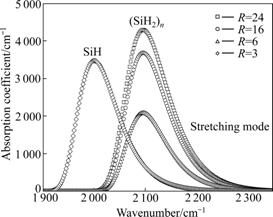
Fig.3 FTIR vibrational spectra of Si:H thin films fabricated at 150 mW/cm2 and different R values
3.3 Raman spectroscopy
Valuable information about the crystalline volume fraction of Si:H thin films can be drawn from data of Raman scattering spectra. A Raman spectrum of a-Si:H thin films is composed of four Gaussian peaks as transverse optic (TO), longitudinal optic (LO), longitudinal acoustic (LA) and transverse acoustic (TA) modes. It is well established that the TO band frequency ��TO and its line width ��TO are associated with the short-range order of the amorphous silicon network. An increase in the short-range order is manifested by a decrease in ��TO and an increase in ��TO [19]. It has also been demonstrated that the ratio of the integrated density ITA/ITO is related to the intermediate-range order and its increase reflects the decrease in the order on this scale. The presence of coordination defects is necessary for the existence of the LA mode and the increase in the integrated intensity of the ILA/ITO ratio indicates an increase in defects in a-Si:H films [20].
The changes of ��TO and ��TO along with Ar dilution ratios are presented in Fig.4(a). With the increase of Ar dilution ratios, ��TO increases simultaneously but ��TO develops quite the opposite. Thus, the improvement of short-range order of the thin films can be concluded from these. Moreover, a sharp change of these parameters can be seen from the graph when R is above 3. This indicates that the structural transformation and the growth of nano-crystal grains do occur around this point. ITA/ITO is decreased with the increase of Ar dilution ratios, and the improvement of intermediate- range order of the thin films can be deduced from this. However, the curve decreases much slower when R is larger than 6. So, as the growth of nano-crystal grains occurs, the effect of Ar dilution on the structural improvement is no longer significant. The decrease of defects in the thin films along with the increase of dilution ratios also happens, and Fig.4(c) can prove this.
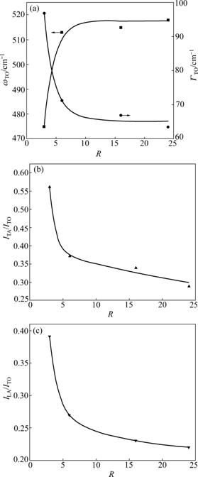
Fig.4 Dependence of Raman features of Si:H thin films on Ar dilution ratios: (a) ��TO, ��TO; (b) ITA/ITO; (c) ILA/ITO
Generally, the Raman spectra of transverse optic (TO) peaks can be best deconvoluted into three Gaussian components as shown in the inter graph of Fig.5. The first scattering in the region of 460-490 cm-1 comes from the TO vibrational modes of amorphous silicon. The second one, intermediate component, arises near 500 cm-1 due to the bond dilation at grain boundaries. The third region at 512-520 cm-1 is assigned to the TO mode of crystal grains of different sizes [21]. Considering the intermediate component (grain boundaries) as a portion of the crystal, the crystalline volume fraction in Si:H thin films can be calculated. The inter graph of Fig.5 shows the deconvoluted peaks of Raman spectrum for the film deposited at R=24 with RF power 150 mW/cm2, and Raman crystalline volume fraction (Fn) is estimated by use of the following formula [22]:
![]() (4)
(4)
where Ia, Ib and In are the integrated intensities of amorphous component, intermediate component and nanocrystalline component, respectively; �� presents ratio of the cross-section of amorphous phase to crystalline phase, which is given by ��=0.1+exp(-D/250), and in this formula D is the grain size in nm [23]. Because the Ar diluted samples have quite small crystal grains, �¡�1.
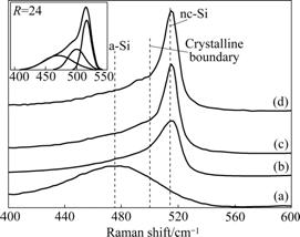
Fig.5 Raman spectra of Si:H thin films deposited at 150 mW/cm2 and different R values (Insert is Gaussian deconvoluted spectra of film deposited at R=24): (a) R=3; (b) R=6; (c) R=16; (d) R=24
The Raman spectra of the thin films prepared at different R values are presented in Fig.5. For R=3, the Raman spectrum is quite broad with a low wave number peak. With the increase of Ar dilution ratio, as to R=6, 16 and 24, the sharpness of the Raman spectrum gradually increases and the higher wave number distribution becomes more narrow. At R=3, the Raman spectrum consists of only one broad distribution at a lower wave number around 475 cm-1, which indicates that the thin films deposited under this condition only consist of amorphous matrix. When the dilution ratio is above 3, a transition from a-Si:H to nc-Si:H growth occurs as indicated by the emergence of the narrow band at 515 cm-1. And, this is in agreement with the results of XRD characterization. Moreover, the increase of the relative intensity of the crystalline peak with the increase of R is also illustrated in Fig.5, and this trend provides useful information about different crystalline volume fractions within the matrix. From the data given in Table 1, the increase of crystalline volume fraction of the films deposited with varied Ar dilution ratios is obvious and significant.
3.4 TEM tests
High resolution TEM images of the films deposited at 150 mW/cm2 and R=24 are taken to observe the mixed-phase region. TEM image clearly shows the surface structures, which contain large amount of nano scale grains, as shown in Fig.6(a).
Moreover, many isolated nano-crystal grains embedded in the amorphous matrix can be seen in Fig.6(b). However, these nano grains are randomly distributed and there is no clear evidence to show distribution or orientation tendency of the nanocrystalline phases as observed in Fig.6. This conclusion is well consistent with XRD analysis. In Fig.6(b), the film is homogeneously amorphous with well-separated dark regions which symbol the nano-crystal grains. And from this graph, the size of grains in the films can be deduced approximately. The average diameter of the dark spots in the graph is about 12 nm. This is in agreement with the discussion above. The corresponding diffraction pattern, the inter graph in the down right corner of Fig.6(b), shows the poly-nanocrystalline nature of the thin film from the clear diffraction rings. These rings correspond to different Si crystal planes. From the graph, three clear light rings emerge homocentrically, corresponding to Si(111), Si(220) and Si(311) from inner to outside respectively. Fig.7 shows the photo of film deposited at 150 mW/cm2 and R=3. No crystal grains can be seen in this photo. The thin film deposited in this condition is amorphous. This confirms the results of XRD and Raman analysis.
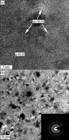
Fig.6 High resolution transmission electron microscopy (HRTEM) graph (a) and diffraction pattern (b) of film deposited at 150 mW/cm2 and R=24
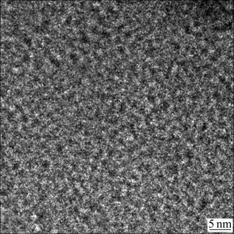
Fig.7 HRTEM graph of film deposited at 150 mW/cm2 and R=3
3.5 UV-visible absorption
The UV-visible absorption coefficient spectra of the thin films at different dilution ratios are shown in Fig.8. It can be seen that the highest optical absorption corresponds to the thin film which is deposited at R=3. When the dilution ratio R increases from 3 to 24, the intensity of the optical absorption coefficient spectra gradually declines. The optical gap (Eg) of the films can be calculated from absorption measurements using Tauc plotting [24]. In this method, (��h��)1/2 is plotted versus h��. The energy-axis intercept of a linear regression line is associated with optical gap Eg. The changes of optical gap depend on the form and the content of hydrogen bonding in the thin films. Comparing the data shown in Fig.9, it can be observed that, when R is increased from 3 to 24, the optical gap decreases from 3.2 to 2.1 eV. The redshift of the optical gap can be explained by an increase of the nano-crystal grain average size when R is increased. And this is in agreement with the XRD results.
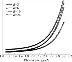
Fig.8 Optical absorption coefficient spectra of films deposited with different R values
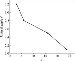
Fig.9 Variation of optical gap with different R values
4 Discussion
Through the studies of XRD, FTIR, Raman and TEM, the following conclusions can be drawn.
(1) Nano-crystal grains start to develop in Si:H thin films when the argon dilution ratio is increased to 6, a relatively low ratio.
(2) The crystalline volume fraction of Si:H thin films increases with the increase of Ar dilution ratio R.
(3) FTIR, Raman and TEM results reveal that the Si:H films embedded with well-separated small nano- crystal grains are still predominantly amorphous.
(4) Hydrogen content is high and the predominant bond is in monohydride mode in the argon diluted Si:H thin films.
(5) The optical absorption coefficient and optical gap of the films decrease with the increase of dilution ratio.
Formation of nano-crystal grains in amorphous network needs certain amount of energy. The change of some deposition parameters facilitates reduction of strain energy at the boundary between nucleation centers and the amorphous matrix by breaking down the strained bonds at the interface and neutralizing of the dangling bonds using high energy plasma from the deposition environment. In our experiments, nano-crystal grains are formed at a moderate RF power density, relative lower substrate temperature in the absence of direct exposure to hydrogen, and especially, a quite lower gas dilution ratio. The role of argon dilution in the growth of nano-crystal grains and amorphous silicon network in the Si:H thin films is discussed in the following paragraphs.
The argon plasma generated by gas discharging under RF power mainly contains two excited radicals, Ar+ and Ar* [15]. A great amount of energy can be transferred to the growth zone of the crystal grains through the bombardment of Ar+ and Ar* radicals. The equilibrium concentrations of Ar+ and Ar* in the plasma and their interaction with atoms in the growth zone determine the magnitude of energy transferred. Actually, in the process of dissociation of SiH4 in the CVD chamber, metastable Ar* plays an important role [25]. Moreover, the bombardment in the growing zone by metastable Ar* also plays a significant role for the reason that its lifetime is of the order of seconds (��1.3 s) [26]. Ar* reacts with SiH4 to form radicals including SiH3, SiH2 and some of the other forms. The reaction rate of Ar* with SiH4 is of the order of 10-10 cm3/s. In comparison, the reaction rate of Ar+ with SiH4 is about one order of magnitude lower [15]. Due to the rate difference, the concentrations of the radicals in the plasma will be different. It has been reported that the change of Ar* concentration is much faster than that of Ar+ [12], which means that Ar* participates in the structure changing process of the Si:H thin films more actively than Ar+.
The concentration of Ar+ mainly depends on the density of RF power for the reason that the ionization energy of Ar follows the electron distribution function. The formation energy of Ar+, which is 15.76 eV is more than that of Ar*, which is 11.5-11.7 eV [25]. Because of the relatively low concentration of Ar+, the film properties have some correlation with the bombardment of Ar*.
The process and amount of energy transmitted by Ar* and Ar+ to the growth zone of nanocrystal grains are also different. The atoms of Ar* will influence the growth of grains only at the thermal velocities which are much lower than the electronic impingement velocity of Ar+. The magnitude of energy transmitted to the lattice is the energy released by the deexcitaton of Ar*. In comparison, the energy transmitted by Ar+ in this process is much tougher. It can be deduced that the energy released by Ar* is absorbed in the lattice which may help the formation of nano-crystal grains. And this contribution is achieved through two processes. The first is that the weak Si��Si bonds are broken up by the energy released from Ar* and this energy may release weakly bonded hydrogen. The second is that the dangling bonds created from weak Si-Si breaking up form strong bonds with other silicon or hydrogen atoms. As consequences, these lead to the increase of SiH bonds and the decrease of voids and strains. Moreover, along with the nanocrystallization of the thin films, the less voids and strains in the materials lead to less light-induced degradation [27].
Si��Si(weak)![]() Si��+��Si (5)
Si��+��Si (5)
Si��+��H![]() SiH (6)
SiH (6)
Si��+��Si![]() Si��Si(strong) (7)
Si��Si(strong) (7)
It has been reported that the increase of argon dilution ratio alone at the same RF power will increase Ar* significantly without much change of Ar+ [12]. With the increase of argon dilution ratio, there will be increasing energy released from deexcitation of Ar*. By replacing weak Si��Si bonds with stronger bonds and removing the hydrogen surrounding the grain centers, some hydrogen-vacuum regions are created. Therefore, more and more hydrogen-vacuum regions appear as a result of the increase of dilution ratio. These regions are fundamental for the growth of crystal grains. So, this model can best explain the changes of grain size, volume fraction of crystallization and content of hydrogen and (SiH2)n with dilution ratio observed in our experiments. And in our present study, the argon dilution ratio at initiating nanocrystallization is quite lower than that reported in Ref.[28].
The hydrogen in Si:H thin films comes from the dissociation of SiH4. The content of hydrogen in the films is dependent on the deposition conditions. In the two-step process discussed above, the weak Si��Si bonds broken by deexcitation of Ar* have a better chance of forming Si��H bonds instead of strong Si��Si bonds. Moreover, the energy released from the Ar* also helps the formation and aggregation of (SiH2)n at crystal boundaries. The appearance and increase of considerable amount of (SiH2)n causes the change of hydrogen content in the thin films. So, according to this model, the increase of Ar dilution ratio at a moderate RF power density will lead to the increase of hydrogen content of the films. This result corresponds to our calculations on the content of hydrogen from FTIR spectroscopy. This model also indicates that the main bulk component of Si:H thin films deposited under argon dilution is still amorphous. This also corresponds to the results from Raman spectroscopy and TEM tests. The formation of small isolated nano-cyrstal grains in the testing thin films is also a result of bond reforming.
A quantum confinement theory that the optical gap depends on the size of nano-crystal grains can explain the redshift of the optical gap when deposition conditions change. The equation proposed by TRWOGA et al [29] for silicon nanoclusters is
![]() (8)
(8)
where c is the confinement constant; Ebg is the bulk silicon bandgap; and �� is the diameter of nano-crystal grains. An increase of the grain size depends on the deposition condition. In our experiments, the increase of dilution ratio results in the increase of grain size. Accordingly, the redshift of the films in optical gap has been observed.
5 Conclusions
(1) Initiation of the growth of nano-crystal grains to crystalline ones occurs at a quite low Ar dilution ratio under a moderate RF power in Si:H thin films. The structural evolution occurs as a result of the increase of Ar dilution ratio when R��3.
(2) The short-range order and the intermediate- range order in Si:H thin films are improved by argon dilution while the defects decrease, and the nano-scale grain size and hydrogen content in the thin films change along with the argon dilution.
(3) The optical properties of Si:H thin films vary with the changes of dilution ratio based on the results from UV-vis measurements.
References
[1] MEIER J, FLUCKIGER R, KEPPNER H, SHAH A. Complete microcrystalline p-i-n solar cell��Crystalline or amorphous cell behavior? [J]. Appl Phys Lett, 1994, 65(7): 860-862.
[2] STAEBLER D L, WRONSKI C R. Reversible conductivity changes in discharge-produced amorphous Si [J]. Appl Phys Lett, 1977, 31(4): 292-294.
[3] FU Y Q, LUO J K, MILNE S B, FLEWITT A J, MILNE W I. Residual stress in amorphous and nanocrystalline Si films prepared by PECVD with hydrogen dilution [J]. Mat Sci Engr B, 124/125(s): 132-137.
[4] VALLAT-SAUVAIN E, KROLL U, MEIER J, SHAH A, POHL J. Evolution of the microstructure in microcrystalline silicon prepared by very high frequency glow-discharge using hydrogen dilution [J]. J Appl Phys, 2000, 87(6): 3137-3142.
[5] LI S B, WU Z M, JIANG Y D, LI W, LIAO N M, YU J S. Structure and 1/f noise of boron doped polymorphous silicon films [J]. Nanotechnology, 2008, 19(8): 085706.
[6] DAS U K, MIDDYA A R, RATH J K, LONGEAUD C, WILLIAMSON D L, CHAUDHURI P. Nanostructures and defects in silicon-hydrogen alloys prepared by argon dilution [J]. J Non-cryst Solids, 2000, 276(1): 46-55.
[7] van ELZAKKER G, NADAZDY V, TICHELAAR F D, METSELAAR J W, ZEMAN M. Analysis of structure and defects in thin silicon films deposited from hydrogen diluted silane [J]. Thin Solid Films, 2006, 511/512(7): 252-257.
[8] BHATTACHARYA K, DAS D. Nanocrystalline silicon films prepared from silane plasma in RF-PECVD, using helium dilution without hydrogen: structural and optical characterization [J]. Nanotechnology 2007, 18(41): 415704.
[9] YOON J H, LEE J Y, PARK D H. Photoluminescence in microcrystalline silicon films grown from argon diluted silane [J]. J Non-cryst Solids, 2004, 338/340(s1): 465-468.
[10] YOUNG D L, STRADINS P, XU Y, GEDVILAS L M, IWANICZKO E, YAN Y, BRANZ H M, WANG Q, WILLIAMSON D L. Nanostructure evolution in hydrogenated amorphous silicon during hydrogen effusion and crystallization [J]. Appl Phys Lett, 2007, 90(8): 081923.
[11] DI Z F, WANG Y Q, NASTASI M, SHAO L, LEE J K, THEODORE N D. Evidence for ion irradiation induced dissociation and reconstruction of Si��H bonds in hydrogen-implanted silicon [J]. Appl Phys Lett, 2008, 93(10): 104-103.
[12] DAS U K, CHAUDHURI P, KSHIRSAGAR S T. Effect of argon dilution on the structure of microcrystalline silicon deposited from silane [J]. J Appl Phys, 1996, 80(9): 5389-5397.
[13] DAS D. Structural studies on Si:H network by Raman, micro-photoluminescence, electron microscopy and ultraviolet ellipsometry: Effect of Ar dilution to the SiH4-plasma [J]. Thin Solid Films, 2005, 476(2): 237-245.
[14] SOPPE W J, DEVILEE C, GEUSEBROEK M, LOFFLER J, MUFFLER H J. The effect of argon dilution on deposition of microcrystalline silicon by microwave plasma enhanced chemical vapor deposition [J]. Thin Solid Films, 2007, 515(19): 7490-7494.
[15] KUSHNER M J. A model for the discharge kinetics and plasma chemistry during plasma enhanced chemical vapor deposition of amorphous silicon [J]. J Appl Phys, 1988, 63(8): 2532-2551.
[16] LANGFORD A A, FLEET M L, NELSON B P, LANFORD W A, MALEY N. Infrared absorption strength and hydrogen content of hydrogenated amorphous silicon [J]. Phys Rev B, 1992, 45(23): 13367-13377.
[17] BRODSKY M H, CARDONA M, CUOMO J J. Infrared and Raman spectra of the silicon-hydrogen bonds in amorphous silicon prepared by glow discharge and sputtering [J]. Phys Rev B, 1977, 16(8): 3556-3571.
[18] LUCOVSKY G, NEMANICH R J, KNIGHTS J C. Structural interpretation of the vibrational spectra of a-Si: H alloys [J]. Phys Rev B, 1979, 19(4): 2064-2073.
[19] MARINOV M, ZOTOV N. Model investigation of the Raman spectra of amorphous silicon [J]. Phys Rev B, 1997, 55(5): 2938- 2944.
[20] LIAO N M, LI W, JIANG Y D, WU Z M, LI S B, LIU Z, LI Z, JIN X, CHEN Y X. Electron irradiation effects on the properties of heavily phosphorus-doped a-Si:H films prepared from undiluted silane [J]. J Phys D, 2008, 41(20): 205412.
[21] VEPREK S, SAROTT F A, IQBAL Z. Effect of grain boundaries on the Raman spectra, optical absorption, and elastic light scattering in nanometer-sized crystalline silicon [J]. Phys Rev B, 1987, 36(6): 3344-3350.
[22] YUE G, LORENTZEN J D, LIN J, HAN D, WANG Q. Photoluminescence and Raman studies in thin-film materials: Transition from amorphous to microcrystalline silicon [J]. Appl Phys Lett, 1999, 75(4): 492-494.
[23] BUSTARRET E, HACHICHA M A, BRUNEL M. Experimental determination of the nanocrystalline volume fraction in silicon thin films from Raman spectroscopy [J]. Appl Phys Lett, 1988, 52(20): 1675-1677.
[24] WOOD D L, TAUC J. Weak absorption tails in amorphous semiconductors [J]. Phys Rev B, 1972, 5(8): 3144-3151.
[25] SANSONNENS L, HOWLING AA, HOLLENSTEIN C, DORIER J L, KROLL U. The role of metastable atoms in argon-diluted silane radiofrequency plasmas [J]. J Phys D, 1994, 27(7): 1406-1411.
[26] MAKABE T, NAKANO N, YAMAGUCHI Y. Modeling and diagnostics of the structure of rf glow discharges in Ar at 13.56 MHz [J]. Phys Rev A, 1992, 45(4): 2520-2531.
[27] STAEBLER D L, PANKOVE J I. Conductivity changes in dehydrogenated and rehydrogenated discharge-produced a-Si:H [J]. Appl Phys Lett, 1980, 37(7): 609-612.
[28] GUPTA N D, RAY P P, CHAUDHURI P, DAS U K, VIGNOLI S, JARDIN C. Study of amorphous to microcry-stalline silicon transformation from argon diluted silane [R]. San Francisco, CA: Materials Research Society, 2002.
[29] TRWOGA P F, KENYON A J, PITT C W. Modeling the contribution of quantum confinement to luminescence from silicon nanoclusters [J]. J Appl Phys, 1998, 83(7): 3789-3794.
Foundation item: Project(60425101) supported by the National Outstanding Young Scientists Foundation of China; Project(06DZ0241) supported by the Science Foundation of General Armament Department of China
Received date: 2010-02-15; Accepted date: 2010-05-18
Corresponding author: LI Wei, Professor; Tel: +86-28-83201123; E-mail: wli@uestc.edu.cn
