
���±��: 1004-0609(2005)08-1214-05
�ſؽ����Ʊ�In2O3-SnO2��Ĥ�����
������, ��ѧ��, �½���
(���пƼ���ѧ ģ���������ص�ʵ����, �人 430074)
ժ Ҫ: ѡ��In2O3��SnO2������1��1�İв�Ϊ����Դ, ���ôſؽ��䷨������ITO��Ĥ, �����˽������ѹǿ�� �������� �����¶ȶԱ�Ĥ���ʺͷ����Ӱ��, ���������������� �о��������: ����ʱ���õ�Arѹǿ�������ڽ���ITO��Ĥ�ĵ�����, ��ȷ��������ѹǿΪ0.2Pa, ���Ϊ120nm��ITO��Ĥ�ڿɼ����������ʿɴﵽ90%; �����������Ըı䱡Ĥ������, ������������0����10L/min(��״̬��, ��ͬ), ������Ũ��(N)����3.2��1020���͵�1.2��1019 /cm3, Nֵ�ı仯��ITO��Ĥ��ѧ��������(Eg)�ı仯������ء� ����ģ����ʵ�����Ǻ�, ��ȷ����ITO��Ĥ�ĵ����Ӳ���(��p=1510nm)�� ��Ĥ�淽���С���ֳ����Եġ�B-M��ЧӦ�� ͨ����������, ������ֱ��ԾǨ��(��E)2ģ��, ��ȷ���˱�Ĥ��Egֵ(3.5~3.86eV)��
�ؼ���: ITO��Ĥ; �ſؽ���; ������; ��B-M��ЧӦ
��ͼ�����: TN304.0255; O484.4
���ױ�ʶ��: A
Preparation and analysis of In2O3-SnO2
thin films deposited by magnetic sputtering
LI Shi-tao, QIAO Xue-liang, CHEN Jian-guo
(State Key Laboratory of Die and Mould Technology, Huazhong University of Science and Technology, Wuhan 430074, China)
Abstract: The ITO thin films were prepared by radio frequency magnetic sputtering using a ceramic target with mass ratio of In2O3 to SnO2 1��1. The experiment parameters such as Ar gas pressure (p(Ar)), oxygen flow rate (f(O2)) and substrate temperature (ts) all have important influence on the transmittance and square resistivity of the thin films. The semiconductor mechanisms of ITO films were studied. The results show that lower p(Ar) can reduce Rs, the optimal p(Ar) of about 0.2Pa was determined. The transmittance of 120nm thick ITO thin films in visible light range is about 90%. The ITO properties can be changed obviously by f(O2), the carrier concentration decrease from 3.2��1020 to 1.2��1019 /cm3 when f(O2) increases from 0 to 10L/min(standard state), which is related to optical forbidden band Eg. And the oscillator model is accorded with the experimental results, the plasma wavelength of ITO films is up to 1510nm.The thin films shows obvious ��Burstin-Moss�� effect due to a decrease in Rs. The direct transition model of (��E)2 versus photon energy Eg was established and a band gap energy Eg was obtained by linear extrapolation.
Key words: ITO thin films; magnetic sputtering; oxygen flow rate; ��Burstin-Moss�� effect
ITOĤ�Ľ�������Ϊ3.75~4.0eV[1-3], ��һ���ڿɼ�����(��=400~780nm)���ԽϺõIJ���, ���Ƿ���ITOĤ���ڡ����ơ�����, һ�����Ų��ӱ�����, �����ձ߽�ġ�B-M������[4]Խ����, �������������ա� �ɼ������� ����߷��������, �䷴����Ҫ�����ڱ�Ĥ�е������������, �����������ɵ�������ġ� ITO��Ĥ�е���������Ҫ�����ֻ���[5, 6]: һ�������Ա�Ĥ�е�����λ, ��һ�������Ա�Ĥ��Sn4+��In3+������Ӷ�������һ�����ӵĹ��ס� ����������In2O3ͨ���������γ�����λת��Ϊ��ITO��Ĥ���й㷺��Ӧ��[7, 8], ������Ϊ���缫�� �ȷ����� ���ܴ��ȡ� ͨ����ΪIn��Sn������Ϊ9��1��ITO��Ĥ�ۺ��������, ������Щ�о���[9]�����˺�SnO2>45%(��������)�ı�Ĥ, �����ֳ����õĹ�����ܡ� ��������ѡ��In2O3�� SnO2������Ϊ1��1�İвĽ��н���(�����������б������߽���ϸ������������ITO��Ĥ��Ӱ�켰�вĺͱ�Ĥ�ɷֵ�һ����), ̽�����Ʊ����նԱ�Ĥ��ѧ���ܵ�Ӱ�졣
1 ʵ��
��ʵ�����ƽ�潦�䷽ʽ, �����豸Ϊ����JPG-450�ſؽ����ǡ� ��Ƭ��Բ�ΰб���ƽ��, �л���Ϊ65mm, ����Ϊ50W, ��ƫѹΪ-120V, ��Ƭ�¶�Ϊ����~300��, ���ѹǿΪ0.2Pa�� �ô���Ϊ99.99%��������ĩIn2O3�� SnO2����������Ϊ1��1�ı������г�ֻ��, ��900���������ѹ�ս�(HIP)��d86mm��8mm�İв�, ѹ��Ϊ150~190MPa, �в�����ܶ�Ϊ97.49%(�����ܶ�Ϊ7.02kg/cm3)�� ��ƬΪ��ͨ�Ƹƹ����β����� ʯӢƬ(24mm��45mm��1.7mm)�͵�����ĵ�����Ƭ, �����ڶ�Ĥ֮ǰ��������ϴ�ɾ��� ����ƫ�Dz�����Ĥ�ĸ�������(�Ե���SiΪ�ĵ�)��ƫ�ǵIJ��������ͨ���ı������IJ����ͽǶȵõ�����, ���ü���������ݴ������������㡣 ��Ĥ����æ�-Step̨����(����Ϊ0.5nm)������ ��Ĥ�����ñ���̽��ϵͳ����, ������UV-2550������ֹ��ȼ�(Shimadzu, �ձ�)���ԡ�
2 ��������
2.1 ��������Ա�Ĥ���ܵ�Ӱ��
Arѹǿ�뱡Ĥ��������(Q)�Ĺ�ϵ�ɱ�ʾΪ[10]
ʽ(1)����, ����һ���Ľ���װ��(Cֵһ��), ��߳������ʵ���Ч��������������ӵ���(I)�� �����ڲ��������ѹ��������, ����I�ͱ����������ѹǿ(p(Ar)), ���ǵ�����ѹǿ����һ��ֵʱ, �����ʿ�ʼ�����½��Ӷ�ʹ�������ʼ�С, Q��(p(Ar))��ϵ��ͼ1��ʾ�� �о�����, p(Ar)����ʹ��Ĥ������Ҳ����, ������Ϊ��������İв����ӱ�Arɢ��ļ��������û���㹻�������ڻ����Ͻᾧ�� Ǩ��, ���Ա�Ĥȱ�ݺ;�������, ����Ե���ɢ���ǿʹ�ñ�Ĥ�ĵ��������ӡ� ͨ�������Ʊ���Ĥ��������Ũ��(N)�ͻ���Ǩ����(��)�IJ���, �������Ž���ѹǿ������, N��1.2��1020���ٵ�8��1019 /cm3, ����10��С��6cm/(V��s), ��һ����������[3]�Ľ���һ�¡� Ϊ�˱�֤���䱡Ĥ����������߱�Ĥ��������, Ӧ����������������ѹǿ����߽�����, ��ѡ��p(Ar)=0.2Pa��
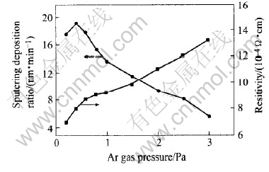
ͼ1 p(Ar)�Խ������ʺ͵����ʵ�Ӱ��
Fig.1 Effects of p(Ar) on deposition ratio and resistivity of ITO films
ͼ2��ʾΪ��Ĥ��������(n)������ϵ��(��)���������Ĺ�ϵ, ͼ2����Ʒ�ĺ�Ⱦ��ɳ������ʺ�ʱ�������60nm�� ��������������f(O2)2L/minʱ���, ԼΪ2.005, Ȼ��������, f(O2)Ϊ6L/minʱ���������(n=2.082)�� ITO��Ĥ������ϵ���ڿɼ��ⷶΧ�ں�С, k��0.1, ����f(O2)��������ֵ��С�� ������Ũ�Ȳ��Ա���������Ũ������f(O2)���Ӷ���3.2��1020���͵�1.2��1019 /cm3, ��Ϊf(O2)�ı��˱�Ĥ������λ��Ũ�Ⱥͱ�Ĥ�ɷ֡� ��������[11, 12]�������ɢģ�ͺ�Drudeģ��, ���Ա�ʾ�������������ѧ�����Ĺ�ϵ, ���Ƕ���ITO��Ĥ����, �������Ƶ��(��p)С�ڿɼ���Ƶ��, ���ֻ����Ϊ���Եķ����ͳ������ơ� ��˱�ʵ������[12]��ģ�Ͳ��������������, ���ݹ��������Ļ����������������ģ��(Oscillator model), ���Ա�ʾΪ
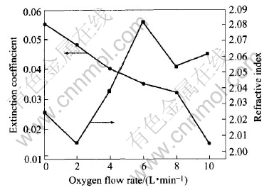
ͼ2 �����������������Ĺ�ϵ
Fig.2 Effects of oxygen flow rate on refractive indexes of ITO films
![]()
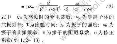
��ʽ(2)���Կ���, ������Ũ�ȵĸı�����(��p)�ı仯�����±�Ĥn�ͦ�ֵ�ĸı䡣 ��0.2Pa�������ѹǿ�� 50WRF���书�ʡ� 2L/min����������, ������120nm��ITO��Ĥ, ���÷ֹ��ȼƲ��������ʺͷ�����, ��ͼ3�е㻮����ʾ, ��A��õ���p=1510nm(���ʺͷ��������ߵĽ�����Ǧ�p)�� ���������� �ӡ� s0�� ��0�� �ü�����[3], ��ʽ(2)����õ������ʺͷ�����������ͼ3��������ʾ, ��B��õ���p=1570nm��

ͼ3 120nm���ITO��Ĥ�����ʺͷ���������
Fig.3 Transmittance(T) and reflectance(R) of 120nm thick ITO film deposited on glass substrate
�ɴ˿ɼ�, ����ģ�ͼ���Ľ����ʵ����ʮ�ֽӽ�, ���ʺͷ�����������״����, ����õ��������Ը���ʵ�ʲ��Ե����ߡ� ����ʽ(2)�ܺõ������ITO��Ĥ�����ʺͷ��������ߡ�
2.2 ��Ĥ����������¶Ⱥ����ʵĹ�ϵ
ͼ4��ʾΪ��Ĥ�ķ��衢 �����¶������ʵĹ�ϵ, ��Ĥ���Ϊ240nm�� ���Կ���, ������¶ȿ�����߱�Ĥ������, �����䷽��, �������ڻ����¶�����, �����㱡Ĥ����������ѧ�������ᾧ���, ȱ�ݼ��١� ���ű�Ĥ����ļ�С, һ���污Ĥ�����ʼ�С; ��һ���污Ĥ�����ս������ŷ���ļ�С��ʼ��UV�����ƶ�, ����Ĥ��������������, ����Ҫ�����ڡ�Burstin-Moss effect��(��ơ�B-M��ЧӦ)[4]����ġ� �ɡ�B-M��ЧӦ����Ŀ����ܴ����Ա�ʾΪ
ITO��Ĥ�ڿɼ��������������ɱ�Ĥ�е�������Ũ�������, ���Ա�Ĥ�����С��Ȼ��������յ���ǿ�� ʽ(3)������Ĥ�е�������Ũ�������±�Ĥ�����Ŀ�����
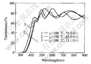
ͼ4 �����¶������ʺͷ���Ĺ�ϵ
Fig.4 Dependence of transmission and square resistance on substrate temperature
2.3 ITO��Ĥ�ܴ��о�
�ı�f(O2)(6�� 8�� 10L/min), ������ʯӢ�����ϳ�����ITO��Ĥ�� ���Ȳ��Ա�Ĥ������ϵ����, �����ͼ5��ʾ, ������(��E)2������ϵ��(��)�Ĺ�ϵͼ(EΪ�����������), Ȼ�������������, ͼ�к�����Ľؾ���ǽ�������Eg��ֵ, ��ͼ6��ʾ�� ���ԾǨ(��E)2/3���Ƶý�������Ei=2.99~3.47eV, ��ֱ��ԾǨ(��E)2ģ�Ͷ�������������Ƶó�Ed=3.5~3.86eV�� ��ͼ5���Կ���, ����������������, ��Ĥ��Eg��С, ���ձ�������ƫ�ơ� Ϊ��˵������ʵ����, ��������[12-14], ��������ͼ7��ʾ���ܴ�ͼ�����͡� �������ּ���, �����ܴ�����, ���������������������ƫ�붯���ռ��, ���Ծʹ�����������ԾǨ�Ļ���:
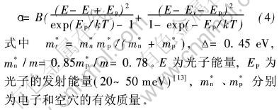
1) ����Ϊֱ��ԾǨʱ, ֱ�ӹ�ѧ����Ed=Eg-4kT(m*n/m*r)+h2(2m*r)-1(3��2n)2/3, ����ϵ����ʾΪ��=A(E-Ed)1/2��
2) ����Ϊ���ԾǨʱ, ��ӹ�ѧ����Ei=��m-��v2=Eg-��-4kT+h22(2m<sub>n)-1(3��2n)2/3, ����ϵ����ʾΪ
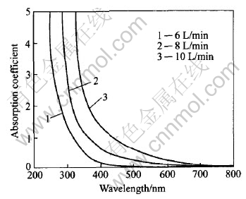
ͼ5 ITO��Ĥ������ϵ��(��)������Ⲩ���Ĺ�ϵ
Fig.5 Relations between optical absorption coefficient(��) and wavelength
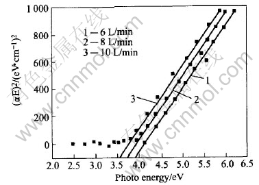
ͼ6 (��E)2���������(E)�Ĺ�ϵ
Fig.6 Relations between (��E)2 and photon energy
��������������ԾǨ���Ʋ�����ͬһ�ܴ�������, ����������ͬ���ܴ�����ԾǨ��, ��ͼ7��1(ITO�ı����ܼ�)��2(ITO���Ӻ���ܼ�)����λ�á� ֱ��ԾǨ��ϵ��ܴ���ʵ�������Ǻ�, ���Ʊ���ITO��Ĥ��ֱ��ԾǨģ��, ���Bashar[14]�ó��Ľ��һ��, ������[15]��Ϊ2/3�η�������������Ͻ���� ����ITO��Ĥ�и��ӵ�ԭ���ṹ���ӵIJ��ӻ���(����λ��Sn4+��In3+���滻)���¶Ա�Ĥ�Ļ�������(������ơ� �ܴ��ṹ��)����ʶ�����ںܴ�IJ���, ���Բ�ͬ���о��ߵó��˲�ͬ����Ͻ���� �ı�������, ����ͬ���ķ�������������, �������, ����������, Egֵ��С, ����Ҫ���ɱ�Ĥ������λ���������[4, 16, 17]�� ��ѧ�������Ⱥͱ�Ĥ��������Ũ���й�, ����Ҫ����Ϊ��Burstain-Moss��ЧӦ�� ʽ(3)������Ĥ�е�������Ũ�������±�Ĥ�����Ŀ�����
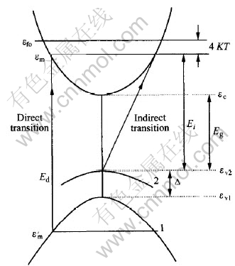
ͼ7 ITO��Ĥ���ܴ��ṹͼ
Fig.7 Diagram of proposed energy band
3 ����
�������ѹǿ�Ա�Ĥ�ij������ʺ͵����������Ե�Ӱ��, ��ʵ���õ����ֵΪ0.2Pa�� �������ı仯����Ĥ������λ�ͳɷֵı仯, �Ӷ����±�Ĥ��������Ũ�Ⱥ������ʵı仯, ����ģ�ʹ������Ͻ�����ITO��Ĥ����������������干��Ƶ�ʵĹ�ϵ, ����ʵ�����һ�¡� ��Ĥ�����¶�����, ��Ĥ�ķ��轵��, �����ֳ����Եġ�Burstain-Moss��ЧӦ�� ͨ���о���Ĥ�Ĺ�ѧ�ܴ�, �������ű�Ĥ������������, ��Ĥ�Ĺ�ѧԾǨ�ܴ���խ, ͨ��������Ϸ���ITO��Ĥ��ֱ��ԾǨ�� ���Ʊ���ITO��Ĥ����Ϊ90%, ����Ϊ13.1��/, Eg=3.5~3.86eV��
REFERENCES
[1] Tahar B H R, Ban T, Ohya Y, et al. Tin doped indium oxide thin films: Electrical properties[J]. J Appl Phys, 1998, 83(5): 2631-2637.
[2] Zhang D H, Ma H L. Room-temperature deposition of indium tin oxide thin films with plasma ion-assisted evaporation[J]. J Appl Phys, 1996, A62: 487-491.
[3] Laux S, Kaiser N, Z��ller A, et al. Room-temperature deposition of indium tin oxide thin films with plasam ion-assisted evaporation[J]. Thin Solid Films,1998, 335: 1-5.
[4] Kim H, Horwitz J S, Kushto G, et al. Effect of film thickness on the properties of indium tin oxide films[J]. J Appl Phys, 2000, 88(10): 6023-6025.
[5] Takaki S, Matsumoto K, Suzuki K. Properties of highly conducting ITO films prepared by ion plating[J]. Applied Surface Science, 1988(33/34): 919-925.
[6] ZENG Ming-gang, CHEN Song-yan, CHEN Mou-zhi, et al. The effects of the microstructure on the optical and electrical quality of indium tin oxide thin films[J]. Journal of Xiamen University (Nature Science), 2004, 43(4): 498.
[7] Cairns D R, White R P ��, Sparacin D K, et al. Strain-dependent electrical resistance of tin-doped indium oxide on polymer substrates[J]. Applied Physics Letters, 2000, 76(11): 1426-1431.
[8] Swint A L, Bohn P W. Effect of acidic and basic surface dipoles on the depletion layer of indium tin oxide as measured by in-plane conductance[J]. Applied Physics Letters, 2004, 84(1): 61-63.
[9] Minami T, Takeda Y, Takata S, et al. Preparation of transparent conducting In4Sn3O12 thin films by DC magnetron sputtering[J]. Thin Solid Films, 1997, 308-309: 13-18.
[10] ��ΰ��. Ĥ���ϵ��Ʊ�ԭ���� ���պ�Ӧ��[M]. ����: ұ��ҵ������, 1998. 49-61.
TANG Wei-zhong. Preparation Principle, Technology and Application of Film Materials[M]. Beijing: Metallurgy Industry Press, 1998. 49-61.
[11] Born M. Optic[M]. Berlin: Springer, 1981. 421.
[12] Hamberg I, Granqvist C G. Evaporated Sn-doped In2O3 films: basic optical properties and applications to energy-efficient windows[J]. Sol Energy Mater, 1986, 14: 241.
[13] Rakhshani A E, Mkdisi Y, Ramazaniyan H A. Electronic and optical properties of fluorine-doped tin oxide films[J]. J Appl Phys, 1998, 83(2): 1056.
[14] Bashar S A. Study of Indium Tin Oxide (ITO) for Novel Optoelectronic Devices[D]. London: University of London, 1998.
[15] �� ��, ��־��, ��ѩ��, ��. ITO��Ĥ��X���߹���ӵ羵�о�[J]. ������ѧ��, 2000, 15(1): 191-194.
CHEN Meng, PEI Zhi-liang, BAI Xue-dong, et al .X-ray photoelectron spectroscopy studies of ITO thin films[J]. Journal of Inorganic Materials, 2000, 15(1): 191-194.
[16] Honda S, Watamori M, Oura K. The effect of oxygen content on electrical and optical properties of indium tin oxide films fabricated by reactive sputtering[J]. Thin Solid Films, 1996, 218-282: 206-208.
[17] Bellingham J R, Mackenzie A P, Phillips W A. Precise measurements of oxygen content: Oxygen vacancies in transparent conducting indium oxide films[J]. Appl Phys Lett, 1991, 58(22): 2506.
������Ŀ: ���пƼ���ѧ���㲩ʿ�����Ļ���������Ŀ(2004-39);����Ԥ�п���ҵ����������Ŀ(51410020401JW0504)
�ո�����: 2005-01-27;
������: 2005-05-05
�����: ������(1978-), ��, ��ʿ�о���.
ͨѶ����: ��ѧ��, ����; �绰: 027-87541540; E-mail: xlqiao@public.wh.hb.cn
(�༭ ������)
