
J. Cent. South Univ. (2012) 19: 299-303
DOI: 10.1007/s11771-012-1004-7![]()
Negative differential resistance behavior in doped C82 molecular devices
XU Hui(���)1, JIA Shu-ting(�����)1, CHEN Ling-na(������)1, 2
1. School of Physics Science and Technology, Central South University, Changsha 410083, China;
2. School of Computer Science and Technology, University of South China, Hengyang 421001, China
? Central South University Press and Springer-Verlag Berlin Heidelberg 2012
Abstract:
By using the first-principle calculations and nonequilibrium Green functions method, the electronic transport properties of molecular devices constructed by C82, C80BN and C80N2 were studied. The results show that the electronic transport properties of molecular devices are affected by doped atoms. Negative differential resistance (NDR) behavior can be observed in certain bias regions for C82 and C80BN molecular devices but cannot be observed for C80N2 molecular device. A mechanism for the negative differential resistance behavior was suggested.
Key words:
electronic transport properties; negative differential resistance; first-principle; molecular device��
1 Introduction
In recent years, the fullerene has attracted intensive interests due to its fundamental properties and potential applications in future electronic devices [1-5]. Doping of the fullerenes is a central issue [6-9]. WANG et al [10] reported the orbital hybridization and charge transfer for the interaction between the cage and the metal atom in Dy@C82 metallfullerenes. LU et al [11] found that La@C82, La2@C80 and Sc3N@C80 are endothermically encapsulated inside the (17,0) nanotube and electron transfer takes place from the nanotubes to strongly electrophilic La@C82 and La2@C80. Previous studies mainly focus on the effect on the electronic structure of single fullerene molecules by endothermal doping, but rarely focus on the effect on electronic properties of single fullerene molecules by substitutional doping. Recently, transport properties of fullerenes molecular devices have been receiving great attentions, because they are the most prospective candidates in the nanoelectronic devices [12]. FAN et al [13], ZHANG et al [14], LI et al [15] observed the negative differential resistance (NDR) in fullerenes molecular devices. NDR effect, which is characterized by the phenomenon of decreasing current with the increase of bias, has gained a wide range of applications including logic circuits [16], memory [17], switching [18] and amplification [19]. Different mechanisms such as chemical changes [20], local orbital symmetry matching between electrodes and scatting region [21], the channel conduction suppressed at a certain bias [22] and the bias-induced alignment of molecular orbit [23] have been proposed to explain the NDR behavior in molecule devices.
In this work, the electronic transport properties for molecular devices constructed by C82, C80BN and C80N2 coupled with carbon nanotubes (CNTs) electrodes were investigated by applying nonequilibrium Green functions in combination with the first-principle theory. Here, C80BN is formed by replacing a pair of carbon atoms of the C82 with a pair of B/N atoms, and C80N2 is formed by replacing a pair of carbon atoms of the C82 with a pair of N atoms. The present work focuses on the effect of doped atoms on the electronic transport properties for molecular devices constructed by C82, C80BN and C80N2.
2 Method and model
The model structures are shown in Fig. 1(a). These devices are divided into three parts including left lead, scattering region and right lead. Both leads are semi-infinite CNTs and scattering region is composed of different molecular configurations (Fig. 1(b)). The structures are optimized and the quantum transport calculations are carried out by using an ab initio code package, ATK. ATK is based on the real space, nonequilibrium Green functions (NEGF) formalism and the density-functional theory (DFT) [24]. After relaxing the structures, the distance between the surface of CNTs of CNTs and the central of C82 is about 5.0 ?. The generalized gradient approximation (GGA) and the Perdew-Wang 91 (PW91) exchange-correlation function are chosen. The electrode calculations are performed under periodical boundary conditions, and Brillouin-zone integration is performed using a 1��1��500 Monkhorst- Pach (MP) grid. Single-�� basis set is used and a mesh cutoff is set to be 150 Ry to save computational time. Test calculations with larger basis set and cutoff energy are also performed, which give almost the same results. The conductance is given within Landauer-B��ttiker formalism [25-26].
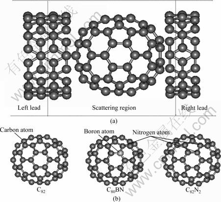
Fig. 1 Schematic views of molecular device and molecules: (a) Molecular device; (b) Molecules
3 Results and discussion
Figure 2 shows the current as a function of the bias voltage for three molecular devices. From Fig. 2, it can be found that all the molecular devices display metallic transport behavior. It can be seen clearly that when the bias is lower than 0.7 V, at the low bias range, the current of C80N2 is the maximum. When the bias 0.8 V�� |Vb|��0.9 V, the sequence of currents is C80BN>C82>C80N2. This means that at very low bias, the introduction of impurity enhances the electron transport. In addition, it is found that when the bias takes a value between -0.9 V and -1.5 V for C82 and when the bias takes a value between -0.9 V and -1.2 V for C80BN, the current decreases with the increases of the bias, which shows that the NDR behavior is in the negative bias range. The peak-to-valley ratios are 1.63 and 1.43 corresponding to C82 and C82BN, respectively. However, the NDR behavior for C82N2 system is not found.
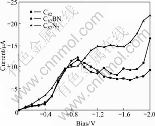
Fig. 2 Curves for currents as function of bias for C82, C80BN and C80N2 molecular devices
To understand the origin of the transport properties of molecular devices, the transmission spectrum T(E, Vb) was presented and the projected densities of states (PDOS) of molecular devices at zero bias (Vb=0) are shown in Fig. 3. Figure 3 shows very distinct transmission spectra for three molecular devices. From Fig. 3(a), it can be found that near Fermi level there are two big transmission peaks which originate from HOMO and LUMO, respectively. Two strong and broad transmission peaks correspond to a strong transmission channel opened in C82 system. When more electrons are introduced into the system, it is clearly observed that LUMO are split into more levels, and more transmission peaks appear in the system (Fig. 3(b)). This may lead to more opened transmission channels. From Fig. 3(c), it can also be found that transmission peaks of C80N2 near the Fermi energy are more than those of C82 and C80BN. Thus, it can be inferred that there is a strong coupling between electrode and molecular orbit, which dominates the electron transport in C80N2 at low bias. This may help explain why the current of the C80N2 system is larger than that of C82 and C80BN at low bias.
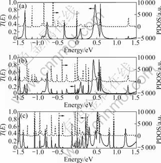
Fig. 3 Transmission coefficient and corresponding PDOS on electron energy at zero bias: (a) C82; (b) C80BN; (c) C80N2
To understand the NDR behavior clearly, the transmission spectrum and the corresponding PDOS of C80, C80BN and C80N2 under different biases are presented in Fig. 4. The region between the solid lines is the bias window and the shade area denotes the integral area in the bias window. As known, the current is determined by T(E, Vb) in the bias window and further determined by the integral area (namely, the shadow area in the bias window). From Fig. 4(a), it can be found that at the bias Vb=-0.9 V, high and broad transmission peaks enter into the bias window. This is the bias corresponding to the maximum current and it denotes the beginning of the NDR. Compared with Fig. 4(a), Fig. 4(b) shows that the total magnitude of transmission coefficient in the bias window becomes smaller, so the NDR behavior appears in C82. This bias (Vb=-1.5 V) is at the minimum current and corresponds to the end of the NDR. From Fig. 4(c), it can be found that at the bias Vb=-1.6 V, new transmission peaks enter bias windows, so the NDR behavior disappears. Compared with C82 system, C80BN system can decrease the peak-to-valley ratio of NDR. From Fig. 5(a) and Fig. 5(b), it can be seen that when the bias takes a value between Vb=-0.9 V and Vb=-1.2 V, the bias window increases with the increase of the bias, but the total integral area gets smaller. As a result, the current decreases and NDR appears. From Fig. 5(c), it can be found that when the bias is further increased, the current increases again and NDR disappears. From Fig. 6, it can be seen that the total integral area increases with the increase of the bias, so there is no NDR in C80N2 molecular device.
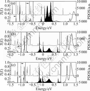
Fig. 4 Transmission coefficient and corresponding PDOS for C82 molecular device under different biases: (a) Vb=-0.9 V; (b) Vb=-1.5 V; (c) Vb=-1.6 V
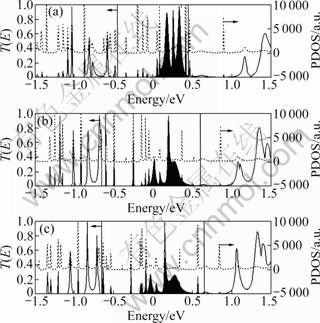
Fig. 5 Transmission coefficient and corresponding PDOS for C80BN molecular device under different biases: (a) Vb=-0.9 V; (b) Vb=-1.2 V; (c) Vb=-1.3 V
In order to further understand the NDR behavior, the molecular projected self-consistent Hamiltonian (MPSH) was presented. Note that MPSH contains the molecule-lead coupling effects, which decides the transport ability of molecular devices. Figures 7 and 8 show two frontier molecular orbits from HOMO to LUMO for C82 and C80BN molecular devices, respectively. From Fig. 7(a) and Fig. 7(b), the contribution of HOMO to transmission decreases with the increase of the bias from -0.9 V to -1.5 V, thus there is less current at -1.5 V compared with that at -0.9 V. Compared with Fig. 7(b), it can be seen from Fig. 7(c) that the contribution of HOMO and LOMO changes a little, but the contribution of additional channels LUMO+1 to transmission increases due to the increase of the chemical potential window, which leads to a higher current at -1.6 V compared with that at -1.5 V. From Fig. 8, it can be found that when bias increases from -0.9 V to -1.3 V, the contribution of LUMO to transmission decreases. But at the bias Vb=-1.3 V, the contribution of additional channels LUMO+1 to transmission increases. According to the above results, it can be concluded that the nonlinear change in the coupling from a bias dependent transition in the broken symmetry phase of the molecular wave function is the origin of the NDR.
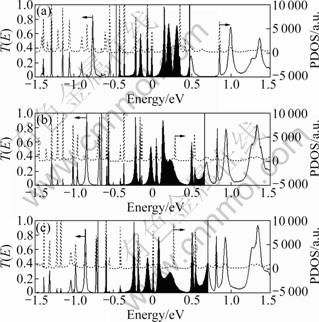
Fig. 6 Transmission coefficient and corresponding PDOS for C82N2 molecular device under different biases: (a) Vb=-0.9 V; (b) Vb=-1.3 V; (c) Vb=-1.4 V
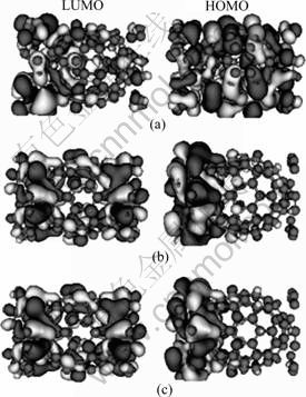
Fig. 7 Frontier orbits of MPSH from LOMO and HOMO for C82 molecular device: (a) Vb=-0.9 V; (b) Vb=-1.5 V; (c) Vb= -1.6 V
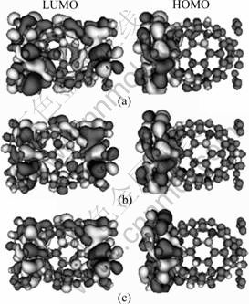
Fig. 8 Frontier orbits of MPSH from LOMO and HOMO for C80BN molecular device: (a) Vb=-0.9 V; (b) Vb=-1.2 V; (c) Vb=-1.3 V
4 Conclusions
1) Using first-principle quantum transport calculations, all the molecular devices display metal transport behavior. At low bias, doping can enhance the electron transport.
2) The calculation in molecular devices reveals NDR features in the I-V curves and B/N pair dope of the C82 molecule can decrease the peak-to-valley ratio.
3) The bias dependent transition in the broken symmetry phase of the molecular wave function leads to a nonlinear change in the coupling between the molecule and lead, triggering the NDR behavior.
References
[1] PALACIOS J J. Coulomb blockade in electron transport through a C60 molecule from first principles [J]. Physical Review B, 2005, 72(12): 125424-1-125424-6.
[2] AN Yi-peng, YANG Chuan-lu, WANG Mei-shan, MA Xiao-guang, WANG De-hua. First-principles study of structure and quantum transport properties of C20 fullerene [J]. The Journal of Chemical Physics, 2009, 131(2): 024311-1-024311-6.
[3] OUYANG Fang-ping, XU Hui, FAN Tou-jiao. All-carbon nanoswitch based on C70 molecule: A first principles study [J]. Journal of Applied Physics, 2007, 102(6): 064501-1-064501-4.
[4] JORN R, SEIDEMAN T. Competition between current-induced excitation and bath-induced decoherence in molecular junctions [J]. The Journal of Chemical Physics, 2009, 131(24): 244114-1- 244114-16.
[5] GARDENER J A, BRIGGS G A D, CASTELL M R. Scanning tunneling microscopy studies of C60 monolayers on Au(111) [J]. Physical Review B, 2009, 80(23): 235434-1-235434-9.
[6] TOTH S, QUINTAVALLE D, NAFRADI B, KORECZ L, FORRO L, SIMON F. Enhanced thermal stability and spin-lattice relaxation rate of N@C60 inside carbon nanotubes [J]. Physical Review B, 2008, 77(21): 214409-1-214409-5.
[7] YANG Shen-yuan, YOON M, HICKE C, ZHANG Zhen-yu, WANG E G. Electron transfer and localization in endohedral metallofullerenes: Ab initio density functional theory calculations [J]. Physical Review B, 2008, 78(11): 115435-1-115435-5.
[8] YANG C K. Magnetic molecules made of nitrogen or boron-doped fullerenes [J]. Applied Physics Letters, 2008, 92(3): 033103-1- 033103-3.
[9] RIVELINO R, MALASPINA T, FILETI E E. Structure, stability, depolarized light scattering, and vibrational spectra of fullerenols from all-electron density-functional-theory calculations [J]. Physical Review A, 2009, 79(1): 013201-1-013201-10.
[10] WANG Ke-dong, ZHAO Jin, YANG Shang-feng, CHEN Lan, LI Qun-xiang, WANG Bing, YANG Shi-he, YANG Jin-long, HOU J G, ZHU Qing-shi. Unveiling metal-cage hybrid states in a single endohedral metallofullerene [J]. Physical Review Letters, 2003, 91(18): 185504-1-185504-4.
[11] LU Jing, NAGASE S, RE Su-yong, ZHANG Xin-wei, YU Da-pen, ZHANG Jin, HAN Ru-shan. Interplay of single-wall carbon nanotubes and encapsulated La@C82, La2@C80, and Sc3N@C80 [J]. Physical Review B, 2005, 71(23): 235417-1-235417-5.
[12] NISHIKAWA T, KOBAYASHI S, NAKANWATARI T, MITANI T, SHIMODA T, KUBOZONO Y, YAMAMOTO G, ISHII H, NIWANO M, IWASA Y. Ambipolar operation of fullerene field- effect transistors by semiconductor/metal interface modification [J]. Journal of Applied Physics, 2005, 97(10): 104509-1-104509-5.
[13] FAN Zhi-qiang, CHEN Ke-qiu, WAN Qing, ZOU B S, DUAN Wen-hui, SHUAI Z. Theoretical investigation of the negative differential resistance in squashed C60 molecular device [J]. Applied Physics Letters, 2008, 92(26): 263304-1-263304-5.
[14] ZHANG Xiao-jiao, LONG Meng-qiu, CHEN Ke-qiu, SHUAI Z, WAN Qing, ZOU B S, ZHANG Yan. Electronic transport properties in doped C60 molecular devices [J]. Applied Physics Letters, 2009, 94(7): 073503-1-073503-3.
[15] LI Y F, KANEKO T, HATAKEYAMA R. High-performance negative differential resistance behavior in fullerenes encapsulated double-walled carbon nanotubes [J]. Journal of Applied Physics, 2009, 106(12): 124316-1-124316-6.
[16] CHEN Jiang-shan, XU Li-ling, LIN Jian, GENG Yan-hou, WANG Li-xiang, MA Dong-ge. Negative differential resistance and multilevel memory effects in organic devices [J]. Semiconductor Science and Technology, 2006, 21(8): 1121-1124.
[17] SU Z S, FUNG M K, LEE C S, LI W L, LEE S T. Memory effect and negative differential resistance in tris-(8-hydroxy quinoline)- aluminum/bathocuproine bilayer devices [J]. Applied Physics Letters, 2008, 93(8): 083301-1-083301-3.
[18] DIMITRAKIS P, NORMAND P, TSOUKALAS D, PEARSON C, AHN J H, MABROOK M F, ZEZE D A, PETTY M C, KAMTEKAR K T, WANG Chang-sheng, BRYCE M R, GREEN M. Electrical behavior of memory devices based on fluorene-containing organic thin films [J]. Journal of Applied Physics, 2008, 104(4): 044510-1-044510-11.
[19] MCWHORTER A L, FOYT A G. Bulk GaAs negative conductance amplifiers [J]. Applied Physics Letters, 1966, 9(8): 300-302.
[20] CHEN J, REED M A, RAWLETT A M, TOUR J M. Large on-off ratios and negative differential resistance in a molecular electronic device [J]. Science, 1999, 286(5444): 1550-1552.
[21] CHEN Lan, HU Zhen-peng, ZHAO Ai-di, WANG Bing, LUO Yi, YANG Jin-long, HOU J G. Mechanism for negative differential resistance in molecular electronic devices: Local orbital symmetry matching [J]. Physical Review Letters, 2007, 99(14): 146803-1- 146803-4.
[22] LI Xiao-fei, CHEN Ke-qiu, WANG Ling-ling, LONG Meng-qiu, ZOU B S, SHUAI Z. Effect of intertube interaction on the transport properties of a carbon double-nanotube device [J]. Journal of Applied Physics, 2007, 101(6): 064514-1-064514-4.
[23] CORNIL J, KARZAZI Y, BREDAS J L. Negative differential resistance in phenylene ethynylene oligomers [J]. Journal of the American Chemical Society, 2002, 124(14): 3516-3517.
[24] OUYANG Fang-ping, XIAO Jin, GUO Rui, ZHANG Hua, XU Hui. Transport properties of T-shaped and crossed junctions based on grapheme nanoribbons [J]. Nanotechnol, 2009, 20(5): 055202-1- 055202-6.
[25] SAHIN H, SEBGER R T. First-principles calculations of spin-dependent conductance of graphene flakes [J]. Physical Review B, 2008, 78(20): 205423-1-205423-4.
[26] YAN Jie-yun, ZHANG Ping, SUN Bo, LU Hai-zhou, WANG Zhi-gang, DUAN Su-qing, ZHAO Xian-geng. Quantum blockade and loop current induced by a single lattice defect in graphene nanoribbons [J]. Physical Review B, 2009, 79(11): 115403-1- 115403-5.
(Edited by HE Yun-bin)
Foundation item: Project(50721003) supported by the National Natural Science Foundation of China; Project(10C1171) supported by the Scientific Research Fund of Hunan Provincial Education Department, China; Project(11JJ3073) supported by the Natural Science Foundation of Hunan Province, China
Received date: 2011-03-04; Accepted date: 2011-09-20
Corresponding author: XU Hui, Professor; Tel: +86-731-88836762; E-mail: cmpxhg@csu.edu.cn
Abstract: By using the first-principle calculations and nonequilibrium Green functions method, the electronic transport properties of molecular devices constructed by C82, C80BN and C80N2 were studied. The results show that the electronic transport properties of molecular devices are affected by doped atoms. Negative differential resistance (NDR) behavior can be observed in certain bias regions for C82 and C80BN molecular devices but cannot be observed for C80N2 molecular device. A mechanism for the negative differential resistance behavior was suggested.
