

J. Cent. South Univ. (2019) 26: 158-167
DOI: https://doi.org/10.1007/s11771-019-3990-1

Electromagnetic emanation exploration in FPGA-based digital design
Van Toan NGUYEN, Minh Tung DAM, Jeong-Gun LEE
E-SoC Laboratory/Smart Computing Laboratory, Department of Computer Engineering, Hallym University, Chuncheon, 24252, Korea
 Central South University Press and Springer-Verlag GmbH Germany, part of Springer Nature 2019
Abstract:
As semiconductor technologies have been shrinking, the speed of circuits, integration density, and the number of I/O interfaces have been significantly increasing. As a consequence, electromagnetic emanation (EME) becomes a critical issue in digital system designs. Electronic devices must meet electromagnetic compatibility (EMC) requirements to ensure that they operate properly, and safely without interference. I/O buffers consume high currents when they operate. The bonding wires, and lead frames are long enough to play as efficient antennas to radiate electromagnetic interference (EMI). Therefore, I/O switching activities significantly contribute to the EMI. In this paper, we evaluate and analyze the impact of I/O switching activities on the EME. We will change the circuit configurations such as the supply voltage for I/O banks, their switching frequency, driving current, and slew rate. Additionally, a trade-off between the switching frequencies and the number of simultaneous switching outputs (SSOs) is also considered in terms of EME. Moreover, we evaluate the electromagnetic emissions that are associated with the different I/O switching patterns. The results show that the electromagnetic emissions associated I/O switching activities depend strongly on their operating parameters and configurations. All the circuit implementations and measurements are carried out on a Xilinx Spartan-3 FPGA.
Key words:
Cite this article as:
Van Toan NGUYEN, Minh Tung DAM, Jeong-Gun LEE. Electromagnetic emanation exploration in FPGA-based digital design [J]. Journal of Central South University, 2019, 26(1): 158�C167.
DOI:https://dx.doi.org/https://doi.org/10.1007/s11771-019-3990-11 Introduction
With recent advanced semiconductor technologies, the feature size of a transistor becomes smaller, therefore, it operates faster and consumes lower power. A lot of features/ functionalities have been integrated into a chip with a large amount of I/O interfaces. In addition, lots of high-speed communication links and high bandwidth applications are currently deployed for modern consumer electronic devices such as online game consoles, high definition multimedia players, etc. Hence, the demand for a high speed data transfer capability between multiple integrated circuits (ICs) through the I/O interfaces has been growing up rapidly. The increase in I/O speed and the number of I/Os, and the shrinking semiconductor technology causing EMI become more difficult to solve. Additionally, the supply voltage has been decreased to meet low power design requirement, which makes the ICs more vulnerable to electromagnetic (EM) noises.
For the past few years, many research works have concerned about EMI associated with the I/O switching activities. PILSOO et al [1] analyzed the influence of the supply voltage variation on the duty cycle and slew rate of the DRAM signals which affect the radiated electromagnetic energy. Actually, when the duty cycle of a signal is changed due to the supply voltage variation, the slew rate of the signal is also changed. Thus, the radiated electromagnetic energy highly depends on the slew rate. KIM et al [2] carried out the prediction of the near field and far field EMI that were associated with I/O switching activities. Then, they validated their proposed model by comparing the measurement and simulation results under two scenarios: the minimum and maximum slew rates. However, their model just performed with one I/O buffer. The mutual influences between I/O buffers, the effect of SSOs, and their impacts on the EM emissions had not been evaluated yet. I/O switching occurs during a data transfer through the I/O interfaces, but the switching produces the voltage drop in a power distribution network (PDN). The noisy voltage propagates into the power network of a chip die, which introduces some fluctuations in the on-chip PDN. That is called simultaneous switching noise (SSN). The impact of SSN on the signal eye diagram of a Universal Serial Bus (USB) interface was measured and analyzed in Ref. [3]. The SSN affects the performance of I/O interfaces. Likely, the SSN and jitter were measured and analyzed in Ref. [4]. The paper was only to clarify the influence of the effective inductance of the package on the jitter of I/O interfaces. SSOs and parasitic package inductance also produce EM noises, which can affect the performance of I/O interfaces, had not considered in Refs. [3, 4].
Different from the previous publications, our paper aims to evaluate and analyze the impact of I/O switching activities on the EM emanation by exploring all the possibly configurable parameters of commercial FPGA I/Os. There are two kinds of I/O interfaces: a single ended interface and a differential interface. OIKAWA et al [5] stated that although high speed interfaces will migrate gradually to differential signaling schemes in the future, single ended schemes are still commonly used. In this work, we carry out all experiments on the single ended interface, namely LVCMOS. In our exploration of design space, we use the I/O supply voltage, the maximum drive strength, the switching frequency, and the slew rate as configurable parameters of the I/O interfaces. Additionally, the joint impact of the SSOs and their switching frequencies, and the I/O switching patterns on the EM emissions are also investigated. The goal of this work is to provide a full picture about the EM emissions that originate from the I/O switching activities in a digital circuit by exploring all their possible configurations.
This paper is organized as follows. Section 2 introduces the overview of electromagnetic emission and near field scanning. The design space exploration is described in Section 3. The experimental results are presented in Section 4. Finally, Section 5 concludes the paper.
2 Overview of electromagnetic emission and near field scanning
Any electrical and electronic devices that have voltage or current changes generate electromagnetic fields to their ambient environments. EMI is a consequence of these unwanted electromagnetic fields that adversely affect the operations of their neighboring ICs or devices. Nowadays, it is easy to find ICs in many applications and products such as consumer electronic devices, vehicles, and airplanes where ICs themselves are not only aggressors but also victims of EM disturbance.
RAMDANI et al [6] reported that I/O switching activities are main concerns to the electromagnetic emissions of ICs since I/O buffers are powered by high supply voltages and consume high currents. Furthermore, interconnections such as bond-wires and package lead frames are long enough to significantly contribute to the parasitic emissions. On the contrary, the interconnections between circuits inside the IC core are too short. IC core switching activities might draw a large amount of current from the power supply at the rising/ falling edges of a clock signal. Nevertheless, the supply voltage of an IC core is normally low, i.e., 1.2 V for 90 nm technology node, or lower supply voltages for advanced technologies such as 65 nm and 45 nm [6]. Therefore, the electromagnetic energy that originates from core activities is normally low. Eventually, the electromagnetic emissions that come from I/O switching activities are still dominant. Therefore, this work focuses on the EM emissions from I/O switching activities.
EM noises can be present in both open and closed spaces such as electronic devices, vehicles, airplanes, and outer space [7]. Figure 1 illustrates the noise sources that originate from I/O switching activities of an FPGA device and printed circuit board (PCB) traces. As we can see, the bond-wires, package lead frames, and PCB traces play significant roles in electromagnetic emissions. These unintentional EM fields can seriously affect the reliability and stability of the circuits. EMI can strike data buses and modify the arrival time of incoming data, which can excessively increase delays in data-paths [8]. EMI even produces some glitches on the clock lines. These glitches can behave as real rising and falling clock edges, which severely affects the circuit behaviors [9]. There are some widely used techniques to reduce EMI such as shielding, filtering, and decoupling capacitors [10�C12]. However, these techniques take extra costs and increased physical spaces.
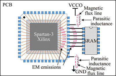
Figure 1 Noise sources originated from I/O switching activities
Understanding and recognizing the hot-spots of the near field (NF) emissions are very necessary for hardware designers in the IC design phase since the reduction of the electromagnetic emissions from an IC helps to reduce the emissions from the system including the IC without any external components such as shielding and filtering [13].
NF scanning is a useful technique to locate the hot-spots of the NF emissions [14�C16]. The measured electric fields and magnetic fields help designers locate the transient current circulation and the corresponding voltage variations on a chip. As stated in Refs. [1, 17], the NF measurement results can be used to estimate the far field radiated emissions. Therefore, in this paper, we perform the magnetic NF scanning to measure the emissions on the FPGA surface. This technique uses a magnetic probe to scan on an IC surface.
For the magnetic NF measurements, the magnetic flux lines originate from the switching operations of the IC and go through the circuit loop of a magnetic probe. Then, they induce a current flowing in the loop. This current also flows through a resistor that is attached to the ends of the probe, which generates an induced voltage. Finally, the probe is connected to a spectrum analyzer to record the spectrum of the NF emissions.
3 Design space exploration
3.1 Hardware implementation
To evaluate the NF emissions generated from the I/O switching, a driving circuit is designed to trigger I/O buffers as demonstrated in Figure 2. This circuit consists of one flip flop (FF) and an inverted feedback path to produce a toggled data pattern of 0-1-0-1. At every rising clock edge, this data pattern is shifted to an output buffer on an I/O bank. When multiple I/Os need to be triggered for NF emission evaluation, this circuit is instantiated. Each circuit is connected to each target I/O buffer. In Figure 2, a Xilinx digital clock manager (DCM) module is utilized to provide the clock source for FFs. Its external reference clock frequency is 50 MHz.
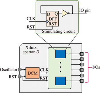
Figure 2 Block diagram of overall design
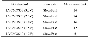
A Xilinx Spartan-3 FPGA supports several I/O standards with different operating voltages from 1.2 V to 3.3 V. The slew rate of I/O buffers can be configured either fast or slow. Moreover, the maximum drive strength of I/O buffers can be selected from a predefined value set. All these configurable parameters can be investigated to find out an appropriate set of parameter values for our target design in terms of low EMI. The configurable parameters of I/O blocks (IOBs) are listed in Table 1.
Table 1 Configurable parameters for IOBs of Spartan-3 FPGA
3.2 Experimental setup
A Xilinx Spartan-3 based FPGA board is powered by three voltage supplies: 1.2 V, 2.5 V, and 3.3 V. The voltage regulator of 1.2 V feeds the internal logic core while the 2.5 V supply feeds the DCMs. The 3.3 V supply is utilized to feed the I/O banks. In our experiments, there are some measurements related to downscaling the supply voltage of I/O banks. Therefore, a programmable DC power supply is utilized to power the I/O banks.
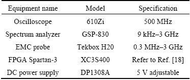
In this work, the NF scanning technique is used to measure the magnetic NF emissions from the I/O switching activities. Therefore, a magnetic probe is connected to a spectrum analyzer to record the spectrum of the emissions. An oscilloscope is used to monitor the waveform at the I/O pins and also to measure the timing parameters of signals. All of the equipment and their specifications are listed in Table 2. The detailed setup for measuring the NF emissions is illustrated in Figure 3.
Table 2 List of equipment and specifications
4 Experimental results and NF emission analysis
4.1 Slew rate of I/O buffer
Practically, an output signal at an I/O pin can be approximated by a trapezoidal wave with finite rising and falling times as shown in Figure 4(a). Slew rate defines how quickly an output can change a logical value, which is inversely proportional to the rising and falling times. To evaluate the impact of the slew rate of I/O buffers on the NF emissions, we implement two designs: 1) I/Os are configured with fast slew rate and 2) slow slew rate. In the experiments, we configure six I/Os to switch concurrently at the frequency of 32 MHz. The switching frequency of I/Os should be different from the reference clock of the DCM (50 MHz) to reduce the effects of external noises on our measurements.
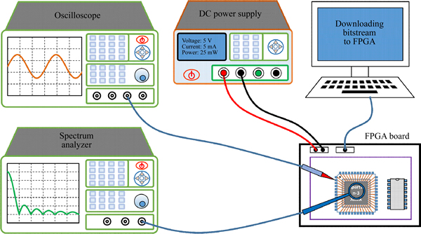
Figure 3 Setup for NF emission measurements
Figure 5 shows the spectrum of NF emissions for the slow and fast slew rates. There are negligible changes in the emission levels between these two configurations at the low frequencies below 100 MHz. From 100 MHz to 1 GHz, the spectrum envelop of the fast slew rate design is higher than the one of the slow slew rate design. The maximum emission level is 91.36 dB����V at 224 MHz for the fast slew rate configuration. This can be explained as follows. Assume that rising and falling times of the output signal are equal. The Fourier expansion coefficients of the periodic trapezoidal signal in Figure 4(a) can be given by Eq.(1) [19].
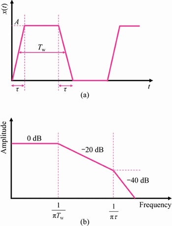
Figure 4 A trapezoidal digital signal (a) and magnitude spectrum for a trapezoidal signal (b) (Tw is pulse width, and �� is the rising/falling time)
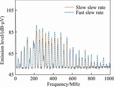
Figure 5 NF emissions of I/O buffers for fast and slow slew rates
 for n��0 (1)
The envelope of the amplitude coefficients for the trapezoidal waveform is shown in Figure 4(b). The harmonic amplitudes fall off with respect to cut-off frequencies. In our case, when changing the slew rate from slow to fast, the duty cycle (Tw) of the output voltage is slightly changed. Therefore, the term M in Eq. (1) is negligibly changed. In the second term N, since |sinc(n��/T)| is less than or equal to |T/(n��)|, so M��|T/(n��)| can be approximated as the upper envelop of the magnitude spectrum. Let ��1 and ��2 be the rising time before and after reducing the slew rate, respectively. As slew rate is inversely proportional to rising time, ��2 is greater than ��1. The approximate reduction rate in the envelop of the magnitude spectrum, ��S, can be derived in Eq. (2). From the analysis, it is expected that the increase of rising/falling time makes the amplitudes of harmonics attenuate, which leads to the reduction in the emission levels of harmonics.

 (2)
(2)
In summary, when increasing the slew rates of I/O buffers, the magnetic NF emission levels of I/O buffers increases. Therefore, we should only use fast slew rate I/O buffers when the timing issue of the design is critical.
4.2 I/O supply voltage
Reducing either the magnitude of electric or magnetic field can lower the total magnitude of the electromagnetic field. Downscaling the supply voltage can lower the peak currents of loads which, in turn, reduces the magnetic field. This section evaluates the relationship between the NF emissions generated by I/O switching activities and their supply voltages. In our experiments, we focus on the LVCMOS I/O standards with the supply voltages of 3.3 V, 2.5 V, 1.8 V, 1.5 V and 1.2 V. Six I/Os are configured to switch simultaneously at the frequency of 16 MHz in the same direction (i.e. all high or low).
Figure 6 shows the NF emission peaks caused by the I/O switching activities when they are powered by different supply voltages. When increasing the supply voltage, the emission levels increase. With the supply voltage of 1.2 V, the emission level is the lowest with 75.64 dB����V. With the supply voltage of 3.3 V, the emission level is highest with 84.40 dB����V. If increasing the supply voltage from 1.2 V to 1.5 V, 1.8 V, and 2.5 V, the emission levels also increase to 76.58, 79.63 and 80.96 dB����V, respectively. So, the emission level is attenuated about 8.76 dB when changing the supply voltage from 3.3 V to 1.2 V.
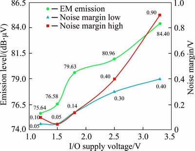
Figure 6 Noise margins and NF emissions of six I/Os switching at 16 MHz
On the other hand, lowering the I/O supply voltage results in reducing the noise margin. The noise margin low (NML) and noise margin high (NMH) are given by Eqs. (3) and (4). VIL(max) and VIH(min) are the maximum and minimum allowable input voltages for logic-0 and logic-1, respectively; VOL(max) and VOH(min) are the maximum and minimum possible output voltages for logic-0 and logic-1, respectively.
 (3)
(3)
 (4)
(4)
The calculated noise margin values NMH and NML are shown in Figure 6. When reducing the power supply voltage, the noise margin values are also decreased. Particularly, with supply voltage of 3.3 V, the noise margin high is 0.9 V, and the noise margin low is 0.4 V. When reducing the supply voltage to 1.2 V, the noise margin high and low decrease to 0.10 V and 0.05 V, respectively. That means the operation of the FPGA at this voltage becomes more susceptible to the EM disturbance.
In short, when reducing the supply voltage, the NF emission level will attenuate. However, decreasing the supply voltage results in the reduction in the noise margins, which can hurt the noise immunity of the IC. Hardware designers can trade-off the NF emission levels and the noise margin levels to select an appropriate supply voltage for I/O banks to optimize their target design.
4.3 I/O current consumption
In this section, the relationship between the NF emissions and the consumed currents of I/Os is investigated. Six I/Os are configured to switch concurrently at 32 MHz in the same direction (i.e., all go high or low). To change the load currents, we change the values of resistors that are connected to these I/O pins. Three configurations have been implemented with the peak consumed currents of 8, 12 and 18 mA.
The measured NF emissions that are generated by six I/Os running at 32 MHz are shown in Figure 7, and the peak emission levels for three configurations are plotted in Figure 8. It is noted that, only the EMI spectrum envelops are shown in these plots. On each curve, the highest peak occurs at the harmonic frequency of 224 MHz. Their values are 93.16, 93.94 and 95.90 dB��V with respect to the current levels of 8, 12 and 18 mA. Therefore, the attenuation in the NF emission level between 18mA-curve and 8mA-curve at their highest peaks is 2.74 dB.
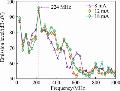
Figure 7 NF emissions at different current consumption levels of I/O buffers
In general, the EMI is diminished when the current consumption is decreased. When a varying current flows along a conductor, the magnetic probe induces a voltage as given in Eq. (5) [20]. �� is the magnetic permeability; I is the loop current; A is the probe area; �� is the angular frequency of the current; d is the distance between the probe and the current source.
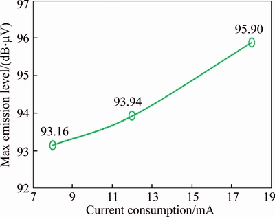
Figure 8 Maximum NF emissions at different currents of I/O buffers
 (5)
(5)
The NF emission level is directly proportional to the loop current. Theoretically, when increasing the current consumption level from 8 mA to 18 mA, the increment in NF emission level should be approximation of 7 dB. However, the actual increment in NF emission is 2.74 dB. The main reason is that the rising and falling time of voltage signals at I/O pins increase when the load currents increase. Particularly, at the current consumption of 18 mA, the average rising and falling time are 9.8 ns while they are 7.45 ns at the current consumption of 8 mA. As discussed in Section 4.1, when the rising time and falling time of a signal increase, the emission levels decrease.
4.4 I/O switching frequency
As indicated by Eq. (5), the NF emission level is proportional to the operating frequency. To assess the relationship between the switching frequencies of the I/O buffers and their NF emissions, four configurations are implemented with six I/O buffers running at 16, 32, 60 and 120 MHz.
The measurement results of the NF emissions from all four configurations are shown in Figure 9. From 16 MHz to 60 MHz, the NF emission levels are increased and nearly proportional to the switching frequency. However, at 120 MHz, the NF emission level is lower than that at 60 MHz. This phenomenon is explained as follows. First, the parasitic components of output buffers such as capacitance and resistance increase filtering effect at higher frequencies. Second, bond-wires and package lead frames are not perfect conductors at the high frequency band. Their self-inductance provides more filtering at higher frequencies. Consequently, the higher frequency signal is attenuated more than the lower frequency signal. The output voltages of I/O buffers cannot have a full swing of 3.3 V when they operate at 120 MHz. Moreover, the effect of filtering results in an increase in the rising/falling time of the signal. These are the reasons why the NF emission level caused by I/O switching activities at 120 MHz is a little lower than that at 60 MHz. Parasitic effects partially decrease the effect of frequency on the NF emissions.
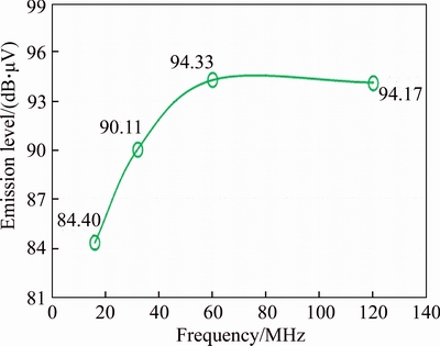
Figure 9 NF emissions at different switching frequencies of I/O buffers
4.5 Switching frequency and number of SSOs
As discussed in Section 4.4, NF emission levels increase when the switching frequency of I/O buffers increases. Besides, when the number of switching I/Os increases, the NF emission levels increase. The bandwidth of a bus line is the number of data bits transmitted per second. Assume that one I/O line represents one data bit. The bus bandwidth is the product of the number of I/Os and their switching frequency as given in Eq. (6). Therefore, while maintaining the I/O bandwidth, we can either 1) decrease the number of I/Os and increase the operating frequency or 2) increase the number of I/Os and decrease the operating frequency. This section is to find the relationship between the number of switching I/Os, their switching frequency, and the NF emission levels generated by their switching activities.
 (6)
(6)
Three configurations have been implemented: (1) sixteen I/Os operate at 16 MHz, (2) eight I/Os operate at 32 MHz, and (3) four I/Os operate at 64 MHz. The measurement results corresponding with three configurations are shown in Figure 10. From these results, we recognize that the NF emission level of the third configuration is the highest while the first one has the lowest level. The emission peaks corresponding with the first and third configurations are 95.50 dB��V and 88.15 dB��V, respectively. The emission reduction rate is about 7.35 dB. Therefore, the first configuration is the best choice in terms of EMI (i.e., increase the number of I/Os and decrease their switching frequency) at the increased expense of hardware resources.
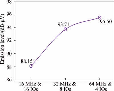
Figure 10 NF emissions for three configurations
4.6 Switching patterns
This section presents the assessment and analysis of the influence of the different switching patterns on the NF emission levels. Two scenarios are experimented: (1) sixteen I/Os toggle between two data patterns 0x0000 and 0xFFFF, and (2) sixteen I/Os toggle between 0x5555 and 0xAAAA as illustrated in Figures 11(a) and (b), respectively. The first configuration is called ��the same direction switching�� while the second one is ��the opposite direction switching��. These sixteen I/Os are configured to switch at 32 MHz, and their loads are the data lines of an off-chip SRAM (max capacitance 8 pF).
The NF emission levels of these two configurations are summarized in Figure 12. Below 700 MHz, the emission levels of the switching in the opposite direction are lower than those of the switching in the same direction at the fundamental frequency and the odd harmonics. In this case, the maximum emission reduction is about 18.54 dB at 96 MHz. In contrast, at the even harmonics, the emission levels of the switching in the same direction are lower than those of the switching in the opposite direction. The maximum NF emission reduction is about 6.02 dB at 576 MHz.
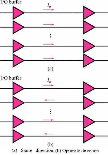
Figure 11 Switching patterns:
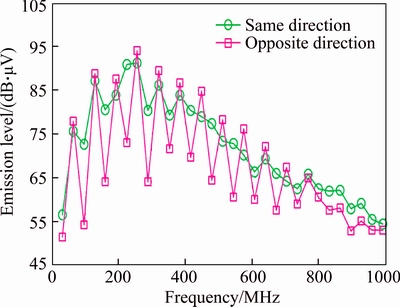
Figure 12 NF emissions for two switching patterns
The Fourier expansion of the voltage signal at one output pin and its out-of-phase counterpart are given by Eqs. (7) and (8). C0 is the DC component; C1��v(��0t) is the fundamental content; Ci (i=2��n) is the Fourier coefficients; Ci��v(i��0t) is the ith harmonic content.
 (7)
(7)
 (8)
(8)
For the opposite direction switching configuration, the fundamental and odd harmonics of two current signals flowing along two adjacent I/O pins are out of phase. Therefore, the magnetic fields travel along with these currents will be canceled out each other. The reduction in emission level is a result of the magnetic field cancellation. However, the complete cancellation cannot be yielded because there is a finite distance between adjacent I/Os and PCB traces. On the contrary, the even harmonics of these currents are in phase. Their magnetic fields will superpose each other. Hence, for the opposite direction switching configuration, the magnetic fields associated with the fundamental and odd harmonic components are canceled each other while the magnetic fields associated with the even harmonics are boosted. Furthermore, the magnetic fields generated by the even harmonics for the opposite direction switching are higher than those for the same direction switching. When all I/O buffers switch in the opposite direction, the output voltages at these I/O pins are a little higher than those whose I/Os switch in the same direction. So, the consumed current peaks are slightly higher.
Finally, from 700 MHz to 1 GHz, the emission levels of the opposite direction switching are lower than those of the same direction one. Due to cross-talk effect, the rising time and falling time of the signals in the opposite direction switching are longer than those of the signals in the same direction switching. The emission levels decrease more rapidly if the slew rate is lower.
5 Conclusions
In this paper, we have evaluated and analyzed the NF emissions related to I/O switching activities by applying six scenarios: the slew rate change, the scaling of I/O supply voltages, the changing of load current consumption, the switching frequency of I/O buffers, the combination of changing switching frequency and the number of I/Os, and the switching patterns.
Slew rate is a main factor that should be considered in the digital circuit design. The NF emission peak generated by the switching activities of the fast slew rate I/Os is 5.32 dB higher than that generated by the slow slew rate ones. Therefore, we should only use fast slew rate in the case of critical timing issue. The supply voltage strongly affects the emission levels of I/Os. By changing the I/O supply voltage from 3.3 V to 1.2 V, the emissions produced by simultaneous switching of six I/O buffers at 16 MHz attenuates about 8.76 dB. However, decreasing the supply voltage causes the I/O interfaces become more sensitive to EMI because their noise margins are also diminished. The impact of I/O currents on their emissions is also investigated. Although the consumed current increases more than 2 times from 8 mA to 18 mA, the NF emission level only increases about 2.74 dB. Once again, the increase in the rising/falling time of the voltage signal significantly deducts the effect of the current consumption on the emission levels. The operating frequency is an important factor that highly affects the NF emissions. If decreasing the switching frequency of I/Os from 60 MHz to 16 MHz, the reduction in emission level is about 9.93 dB. It is worthy to take into account a trade-off the number of I/Os and their operating frequency. From the EMI point of view, with the same bandwidth, it is better to decrease the switching frequency and increase the number of I/Os to reduce the EM emission level. Finally, the emissions related to the different I/O switching patterns have been assessed and analyzed. The experimental results showed that the same direction switching is not always the worst case in terms of EMI. Below 700 MHz, the NF emission peaks of the opposite direction switching are higher than those of the same direction switching.
References
[1] PILSOO L, JAE K L, KYOO Y L, INCHAE S, BOO G K. Analysis of EMI dependence on signal duty and supplied voltage [C]// IEEE Workshop on Signal Propagation on Interconnects. Strasbourg: IEEE, 2009: 1�C4.
[2] KIM N K, HWANG J S, KIM S Y. EMI prediction of slew-rate controlled I/O buffers by full-wave and circuit Co-simulation [J]. Journal of Semiconductor Technology and Science, 2014, 14(4): 471�C477.
[3] CHAN R S, TAN N F, MOKHTAR M R. Simultaneous switching noise impact to signal eye diagram on high-speed I/O [C]// 4th Asia Symp on Quality Electronic Design. Penang: IEEE, 2012: 200�C205.
[4] HARUYA F, YO I, TOSHIO S. Measurement and analysis of SSN and Jitter of FPGA [C]// 2012 Int Symp on Electromagnetic Compatibility. Rome: IEEE, 2012: 1�C6.
[5] OIKAWA R, GOPE D, JANDHYALA V. Return-path extraction technique for SSO analysis of low-cost wire-bonding BGA packages [J]. IEEE Transaction on Components, Packaging and Manufacturing Technology, 2012, 2(4): 677�C686.
[6] RAMDANI M, SICARD E, BOYER A, DHIAS B, WHALEN J J, HUBING T H, COENEN M, WADA O. The electromagnetic compatibility of integrated circuits-past, present, and future [J]. IEEE Transaction on Electromagnetic Compatibility, 2009, 51(1): 78�C100.
[7] TAKUYA S, KUMPEI Y, HIDEHIRO T, KOJI N, MAKOTO N. An extended direct power injection method for in-place susceptibility characterization of VLSI circuits against electromagnetic interference [J]. IEEE Transaction on VLSI Systems, 2015, 23(10): 2347�C2351.
[8] LEE J G. A low EMI circuit design with asynchronous multi-frequency clocking [J]. IEICE Transactions on Electron, 2014, E97-C(4): 1158�C1161.
[9] KUMAR S, CHELLAPPA S, CLARK L T. Temporal pulse-clocked multi-bit flip-flop mitigating SET and SET [C]// 2015 IEEE Int Symp on Circuits and Systems (ISCAS). Lisbon: IEEE, 2015: 814�C817.
[10] FUJITA H, TAKATANI H, TANAKA Y, SHOHEI K, MASAOMI S, TOSHIO S. Evaluation of PDN impedance and power supply noise for different on-chip decoupling structures [C]// 9th International Workshop on EMC of Integrated Circuit. Nara: IEEE, 2013: 142�C146.
[11] YASUHIRO O, MASANORI H, TOSHIKI K, TAKAO O. Supply noise suppression by triple-well structure [J]. IEEE Transaction on VLSI Systems, 2013, 21 (4): 781�C785.
[12] CARR J J. The technician��s EMI handbook: Clues and solutions [M]. Massachusetts: Newnes, 2000.
[13] PARK H H, JANG H T, PARK H B, CHEOLSEUNG C H. An EMI evaluation method for integrated circuits in mobile devices [J]. IEEE Transaction on Electromagnetic Compatibility, 2013, 55 (4): 780�C787.
[14] FANG Wen-xiao, SHI Chun-lei, CHEN Li-hui, EN Yun-fei, LIU Yuan, XIAO Qing-zhong. Near field characterization of the electromagnetic interference for a microcontroller [C]// 2014 Int Conference on Reliability, Maintainability and Safety (ICRMS). Guangzhou: IEEE, 2014: 32�C35.
[15] LECA J P, FROIDEVAUX N, DUPRE P, GILLES J, HENRI B R. EMI measurement, modeling, and reduction of 32-Bit high-performance microcontrollers [J]. IEEE Transaction on Electromagnetic Compatibility, 2014, 56(5): 1035�C1044.
[16] ALAELDINE A, LACRAMPE N, BOYAER A, PERDRIAU R, GAIGNET F, RAMDANI M, SICARD E, DRISSI M. Comparison among emission and susceptibility reduction techniques for electromagnetic interference in digital integrated circuits [J]. Elsevier Microelectronics Journal, 2008, 39: 1728�C1735.
[17] GAO Xu, FANG Jun, ZHANG Yao-jiang, HAMED K, DAVID P. Far-field prediction using only magnetic near-field scanning for EMI test [J]. IEEE Transaction on Electromagnetic Compatibility, 2014, 56(6): 1335�C1343.
[18] DC and switching characteristics (Spartan-3 FPGA family Datasheet) [R]. San Jose: Xilinx Inc., 2013.
[19] SWAMINATHAN M, ENGIN A E. Power integrity modeling and design for semiconductors and systems [M]. Massachussetts: Prentice Hall, 2007.
[20] DENG S, HUBING T, BEETNER D. Analysis of chip-level EMI using near-field magnetic scanning [C]// 2004 Int Symp on Electromagnetic Compatibility. Sendai: IEEE, 2004: 174�C177.
(Edited by HE Yun-bin)
���ĵ���
����FPGA������Ƶĵ�ŷ���̽��
ժҪ�����Ű뵼�弼���IJ���ή������·���ٶȡ������ܶȺ�I/O�ӿڵ������������ӣ���ˣ���ŷ���(EME)��Ϊ����ϵͳ����е�һ���ؼ����⡣�����豸���������ż�����(EMC)��Ҫ����ȷ�����������У��Ҳ��ܸ��š�I/O�������ڹ���ʱ���Ĵ�����������ߺ����߿��㹻����������Ϊ��Ч�����߷����Ÿ���(EMI)����ˣ�I/O������Ե�Ÿ���������Ӱ�졣���Ķ�I/O������Ե�Ż�����Ӱ����������ۺͷ������ı��·���ã���I/O��Ĺ����ѹ�����ǵĿ���Ƶ�ʡ�����������ת���ʡ����⣬�������˽���Ƶ����ͬʱ�������(SSOs)����֮���Ȩ�����⡣���⣬���������벻ͬI/O����ģʽ��صĵ�ŷ��䡣�����������I/O���ػ��صĵ�ŷ���ǿ�����������ǵĹ������������á����е�·ʵ�ֺͲ���������Xilinx Spartan-3 FPGA�Ͻ��еġ�
�ؼ��ʣ���Ÿ��ţ���ŷ��䣻�����ŷţ��ֳ��ɱ�������У�ת������
Foundation item: Project(2018R1D1A1B07043399) supported by Basic Science Research Program through the National Research Foundation, Korea
Received date: 2017-10-24; Accepted date: 2018-07-06
Corresponding author: Jeong-Gun LEE, PhD, Professor; Tel: +82-33-248-2312; E-mail: jeonggun.lee@hallym.ac.kr; ORCID: 0000- 0001-6218-4560
Abstract: As semiconductor technologies have been shrinking, the speed of circuits, integration density, and the number of I/O interfaces have been significantly increasing. As a consequence, electromagnetic emanation (EME) becomes a critical issue in digital system designs. Electronic devices must meet electromagnetic compatibility (EMC) requirements to ensure that they operate properly, and safely without interference. I/O buffers consume high currents when they operate. The bonding wires, and lead frames are long enough to play as efficient antennas to radiate electromagnetic interference (EMI). Therefore, I/O switching activities significantly contribute to the EMI. In this paper, we evaluate and analyze the impact of I/O switching activities on the EME. We will change the circuit configurations such as the supply voltage for I/O banks, their switching frequency, driving current, and slew rate. Additionally, a trade-off between the switching frequencies and the number of simultaneous switching outputs (SSOs) is also considered in terms of EME. Moreover, we evaluate the electromagnetic emissions that are associated with the different I/O switching patterns. The results show that the electromagnetic emissions associated I/O switching activities depend strongly on their operating parameters and configurations. All the circuit implementations and measurements are carried out on a Xilinx Spartan-3 FPGA.
