
Trans. Nonferrous Met. Soc. China 23(2013) 80-85
Microstructure and properties of electronic packaging box with high silicon aluminum-base alloy by semi-solid thixoforming
Qi-jin JIA1, Jun-you LIU1, Yan-xia LI1,2, Wen-shao WANG1
1. School of Materials Science and Engineering, University of Science and Technology Beijing, Beijing 100083, China;
2. Department of Materials, North China Institute of Aerospace Engineering, Langfang 065000, China
Received 7 November 2011; accepted 14 May 2012
Abstract:
The electronic packaging box with high silicon aluminum-base alloy was prepared by semi-solid thixoforming technique. The flow characteristic of the Si phase was analyzed. The microstructures of different parts of the box were observed by optical microscopy and scanning electron microscopy, and the thermophysical and mechanical properties of the box were tested. The results show that there exists the segregation phenomenon between the primary Si phase and the liquid phase during thixoforming, the liquid phase flows from the box, and the primary Si phase accumulates at the bottom of the box. The volume fraction of primary Si phase decreases gradually from the bottom to the walls. Accordingly, the thermal conductivities of bottom center and walls are 107.6 and 131.5 W/(m��K), the coefficients of thermal expansion (CTE) are 7.9��10-6 and 10.6��10-6 K-1, respectively. The flexural strength increases slightly from 167 to 180 MPa. The microstructures and properties of the box show gradient distribution overall.
Key words:
high silicon aluminum-base alloy; electronic packaging; semi-solid thixoforming; thermal conductivity; coefficient of thermal expansion;
1 Introduction
The packaging box is an important structural part used for integrated circuit (IC) seal and signal transmission. It plays shock absorption, protection and cooling effect on components installed internal especially chips. With the rapid development of high-power and highly integrated circuit, substantial raising in chip speed as well as increasingly lightweight on electronic components, the package box needs high thermal conductivity, proper coefficient of thermal expansion (CTE) matching with chips and lower density [1,2]. High silicon aluminum-based electronic packaging materials have advantages of high thermal conductivity, low CTE, low density, easy machining, etc, becoming an ideal material for high-precision packaging box [3-7]. The traditional technology for packaging box was first used to prepare substrate material, which would be connected with the wall material by welding methods [8], such as the packaging box prepared by OspreyMetal Company using spray deposition method. Al-70%Si alloy substrate and Kovar alloy were welded together after the use of brazing [9]. As Kovar alloy and high silicon aluminum alloy have large differences in welding and CTE, welding technique is demanded and thermal stress easily forms at the joints, causing leakage, cracking and other issues. Powder metallurgy, liquid infiltration and other technologies can achieve near-forming packaging, but the process is complex, equipment, molds and tooling are strict and restrictions exist in near net forming of large size box [10,11]. In this work, the electronic packaging box of near-forming was prepared by semi-solid thixoforming. The distribution of Si phase at the bottom and walls, thermophysical properties and mechanical properties of the packaging box were analyzed.
2 Experimental
Intermediate frequency furnace was chosen to melt Al-25%Si (mass fraction) alloy billets with industrial aluminum and silicon. The melting temperature was 850-920 ��C. The alloy was modified with Al-17.6Si-4.6P alloy after refining and degassing by argon gas. Ingots with a size of 120 mm��70 mm��50 mm from billets were treated at 590 ��C for 30 min to obtain the semi-solid slurry. The thixoforming process was applied to the slurry in the home-made mold system at a pressure of 20 MPa and holding time of 5 min.
The box prepared by semi-solid thixoforming was annealed at 490 ��C for 3 h followed by furnace cooling. The microstructures of the box were characterized using an NEOPHOT21 type optical microscope (OM). The morphologies of Si phase and fracture morphologies of the cross-section were observed using an LEO-1450 type scanning electron microscope (SEM). Thermal conductivity measurements were performed on the JR-3 analyzer (NETZSCH Corporation) at 50 ��C, and the sample size was d10 mm��3 mm. CTE measurements were conducted on a DIL 402C (NETZSCH Corporation) thermal expansion instrument protected by nitrogen ambient atmosphere at a heating rate of 5 ��C/min, and the sample size was d5 mm��25 mm. The density was measured based on Archimedes drainage method. The bending strength was tested by an electronic universal testing machine (model RG 3000A), and the sample size was 2 mm��4 mm��36 mm. Brinell hardness was tested by an HBRV-187.5 hardness tester under a load of 612.5 N, and the diameter of the pressure head was 2.5 mm.
3 Results and discussion
3.1 Microstructure
The as-cast micro structure of Al-25%Si alloy is shown in Fig. 1. After the modification with Al-17.6Si-4.6P master alloy, the primary Si distributes homogeneously in Al matrix and the shape is mostly irregular bulk. The eutectic Si is acicular. The sample has compact structure and there are no obvious defects like holes and inclusion.
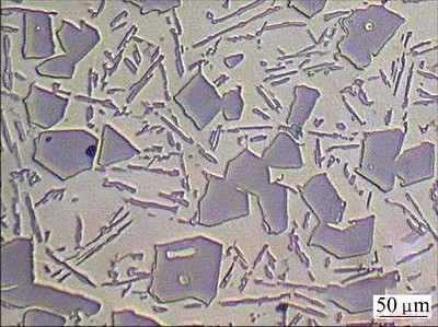
Fig. 1 Microstructure of as-cast Al-25%Si alloy
The electronic packaging box was prepared by semi-solid thixoforming. Through simple machining, the sample is shown in Fig. 2. The bottom size is 120 mm��60 mm��7 mm, the sizes of left and right walls are 100 mm��8 mm��8 mm, and the sizes of the top and down walls are 60 mm��10 mm��8 mm. The sample has structured appearance, good machinability and no obvious defects. The microstructure was observed from metallographic sample taking along the bottom surface of the box center (see point O in Fig. 2) to the edge (Fig. 2, arrows A and B). The microstructures along directions A and B are shown in Figs. 3 and 4, respectively. As shown in the figures, the volume fraction of primary Si phase increases significantly by semi-solid thixoforming. With quantitative metallographic analysis, the metallographs from the bottom center (point O) at different distances were tested. The results are represented in Table 1. The volume fraction of Si phase (point O, 65%) gradually decreases with increasing distance from the bottom center.
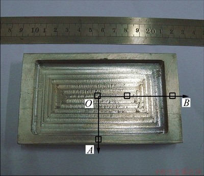
Fig. 2 Electronic packaging box prepared by semi-solid thixoforming
Table 1 Distribution of Si phase at different distances
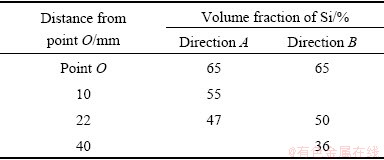
Figure 5 shows the microstructures along the height direction of the box wall. The volume fraction of primary Si decreases along the direction and the results of quantitative analysis show the volume fraction of Si phase amounts for about 43% in Fig. 5(b) and 28% in Fig. 5(c).
As seen from Figs. 3-5, the content of primary Si phase in any area of the box is different, while the matrix morphology is markedly different correspondingly. In the tissue (Figs. 3(a) and (b), Figs. 4(a) and (b)), of which primary Si phase amounts for over 50% (volume fraction), the matrix structure has very little short rod-shaped eutectic silicon. With decreasing the primary Si content, the amount of eutectic silicon of the matrix structure gradually increases, and the morphology becomes thinner and longer. In Figs. 4(c) and 5(c) eutectic silicon has thin fibrous distribution.
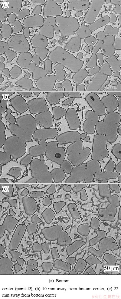
Fig. 3 Microstructures of box along direction A
According to the theory of semi-solid processing [12], the flow patterns of solid and liquid phases are different in the plastic deformation. Solid particles mostly happen to be plastic deformation and solid-slip, while the liquid phase is dominated by flowing. The primary silicon phase mainly distributes in the solid phase. When semi-solid forming occurs, two phases are separated from each other. The liquid phase is extruded from the gap of solid particles and firstly flows to the top or edge of the box. The solid particles are mainly concentrated in the center of the box. Thus, the volume fraction of primary Si decreases along the bottom center to the walls. The eutectic silicon phase mainly distributes in liquid phase. After the deformation, the content of eutectic Si reduces with liquid decreasing at the center of the sample, while in the wall of the sample, the amount of eutectic Si increases because of the accumulation of much liquid.
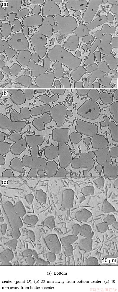
Fig. 4 Microstructures of box along direction B
3.2 Performance analysis
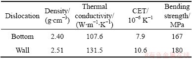
The hardness distribution from the bottom center (Fig. 2, point O) at various distances is shown in Fig. 6. It can be seen that the hardness gradually decreases from the center to the edge. The hardness at the center of the box is over HBw 192, and the hardness of the box wall is HBw 88 in average. After taking samples from bottom center and the box wall, the density, thermal conductivity and CTE were measured. The results are shown in Table 2. It reveals that the densities of the center and walls are basically close, in the range of 2.40-2.51 g/cm3. The center part has a low CTE and proper thermal conductivity. The walls have high thermal conductivity of 131.5 W/(m��K), but CTE increases to 10.6��10-6 K-1. The bending strength of the center part is lower than that of the walls.
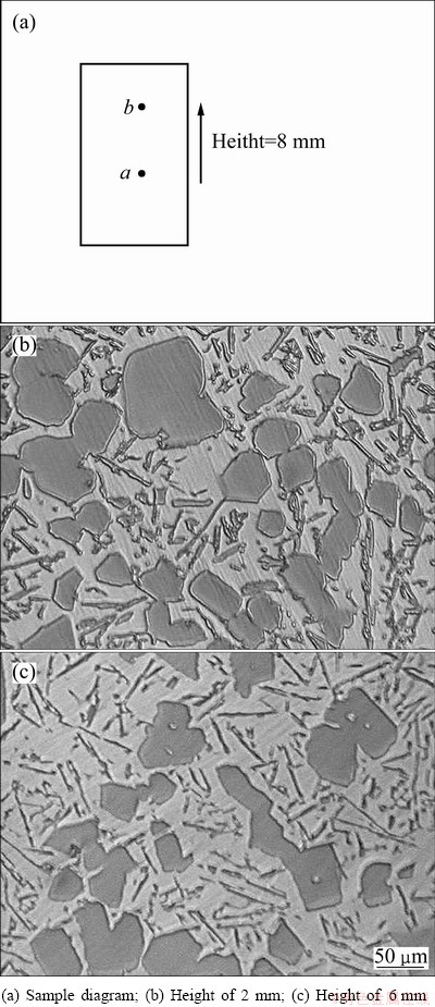
Fig. 5 Microstructures of box along height direction of box wall
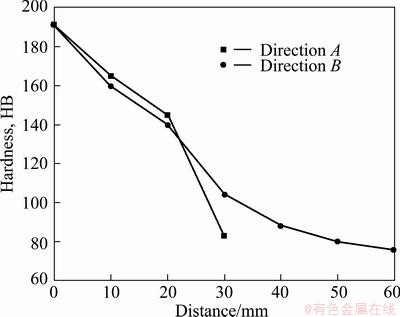
Fig. 6 Hardness curves of box from bottom center at different distances
Table 2 Performance comparison between bottom center and wall
In the electronic packaging process, the underside of the box is mainly used to install the semiconductor chips and miniature components [13]. As a semiconductor circuit substrate, the box requires low CTE matching with Si, GaAs and other chip materials to ease the thermal cycling and stress caused by the mismatch of CTE and to ensure chip with stable performance and durability. In addition, high-speed operation on the circuit will generate a certain amount of heat, and the substrates are required to have good thermal conductivity to release the heat in time. Usually, the box needs to weld with Kovar alloy together after chips are loaded, requiring the box walls to have a good weldability, but Al-Si alloys with high Si content (w(Si)=60%) is difficult to weld with other materials directly [14-16]. The underside of the electronic packaging box prepared by semi-solid thixoforming has low CTE and good thermal conductivity. The wall surface has good weldability because the content of Si phase is very low.
Table 3 shows the performance comparison among the box material and other materials commonly used for electronic packaging. As shown in Table 3, Al-Si alloy with high Si content has low CTE near to that of BeO and GaAs, its thermal conductivity is five times as large as that of the Kovar alloy, and its density is 1/6 that of W-Cu alloy. The integrated performance of the box is excellent.
The results from three-point bending test reveal that the fracture mode is brittle fracture of Si phase and ductile fracture of Al phase. As shown in Fig. 7, the fractures of the bottom center and walls are mainly brittle fractures.
Table 3 Performance comparison among box material and other packaging materials
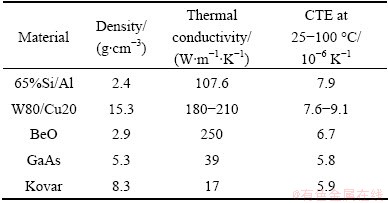
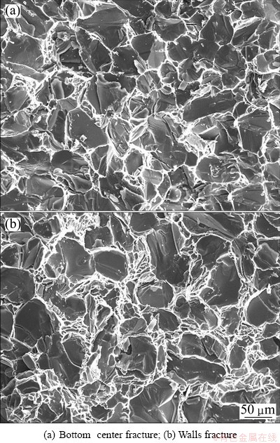
Fig. 7 Three-point bending fracture morphologies
4 Conclusions
1) High performance electronic packaging box with high Si content is successfully prepared by liquid-solid separation. The box has the advantages of compact microstructure, no obvious defects such as holes and inclusion, easy machining, and low production costs.
2) During the semi-solid thixoforming, liquid and Si phase flow separately, the Si phase gathers in the box, which causes the volume fraction of primary Si decreasing gradually from the bottom to the walls. The CTE at the bottom matches with that of the chip material definitely. The walls have high thermal conductivity.
References
[1] ZHANG Hai-po, RUAN Jian-ming. The development of materials and technology of electronic packaging [J]. Materials Science and Engineering of Powder Metallurgy, 2003, 8(3): 216-223. (in Chinese)
[2] LI Chao, PENG Chao-qun, YU Kun, WANG Ri-chu, YANG Jun, LIU Rong. Microstructure and properties of spray deposition 70%Si-Al alloy for electronic packaging applications [J]. The Chinese Journal of Nonferrous Metals, 2009, 19(2): 303-306. (in Chinese)
[3] GAN Wei-ping, CHEN Zhao-ke, YANG Fu-liang, ZHOU Zhao-feng. Research status and development of high silicon aluminum alloy for light weight electronic package materials [J]. Materials Review, 2004, 18(6): 79-82.
[4] CUI C, SCHULZ A, SCHIMANSKI K, ZOCH H W. Spray forming of hypereutectic Al-Si alloys [J]. Journal of Materials Processing Technology, 2009, 209: 5220-5222.
[5] ZHANG Ji-shan, WANG Feng, YANG Bin, CUI Hua, DUAN Xian-jin. A method of spray deposition high silicon aluminum alloy: China, CN00124660.7 [P]. 2002-04-24. (in Chinese)
[6] MA Chun-mei, WANG Kai-kun, XU Feng, YANG Quan, ZHANG Qi. Study on the thixoforming of electronic packaging box with SiCp and Al alloy [J]. Electronic Components and Materials, 2009, 28(6): 60-63. (in Chinese)
[7] GAN Wei-ping, LIU Hong, YANG Fu-liang. Microstructures and mechanical properties of high silicon aluminum alloy affected by different process [J]. Materials Review, 2006, 20(3): 127-128.
[8] ZHANG Dong-ming, ZHANG Lian-meng, GU Xiao-feng, YANG Jun. A preparation method of high conductivity electronic packaging box with laser weldability: China, CN200610125306.5 [P]. 2007-05-30. (in Chinese)
[9] LI Zhi-hui, ZHANG Yong-an, XIONG Bai-qing, LIU Hong-wei, WEI Yan-guang, ZHANG Ji-shan. Plating and brazing performance of spray-formed Si-Al materials for electronic packaging [J]. Chinese Journal of Rare Metals, 2010, 34(5): 633-637.
[10] LI Yan-xia, ZHANG Ju-cheng, LIU Jun-you, LIU Guo-quan. Research progress on electronic package with lightweight, high silicon content aluminum silicon alloy [C]// LIU Guo-quan. Proceeding of the 7th National Conference on Material Science and Image Technology. Beijing: Chinese Society for Stereology, 2009: 204-209. (in Chinese)
[11] CAI Yang, ZHENG Zi-qiao, LI Shi-chen, FENG Xi. The technique and mechanism to fabricate lightweight Si-Al composites for electronic packaging [J]. Powder Metallurgy Technology, 2004, 22(3): 168-169. (in Chinese)
[12] KANG Yong-lin, MAO Wei-min, HU Zhuang-qi. The theory and technology of semi-solid metal processing [M]. Beijing: Science Press, 2004: 90-100. (in Chinese)
[13] WANG Kai-kun, KANG Yong-lin, SONG Pu-guang. Preparation of SiCp/A356 electronic packaging materials and its thixo-forging [J]. Transactions of Nonferrous Metals Society of China, 2010, 20: 988-992.
[14] YANG Pei, YU Zhi-shui, QI Kai, YU Chun, LI Rui-feng. Mechanisms of cracks forming in Al203/Kovar brazing joint [J]. Journal of East China Shipbuilding Institute, 2005, 19(1): 86-88. (in Chinese)
[15] YANG Hui-juan, WANG zhi-fa, JIANG Guo-sheng, WANG Hai-shan, TANG Ren-zheng. Preparation of Kovar/Cu/Kovar laminates by rolling combination [J]. Rare Metals and Cemented Carbides, 2004, 32(2): 7-8. (in Chinese)
[16] YU Zhi-hua, ZHANG Jian-yun, ZHOU Xian-liang, ZOU Ai-hua. Research and development on thermal conductivity of SiC/Al composites applied to electronic packaging [J]. Metallic Functional Materials, 2009, 16(1): 61-63. (in Chinese).
���̬��������Ʊ��߹��������ӷ�װ�������֯������
�����1��������1������ϼ1,2��������1
1. �����Ƽ���ѧ ���Ͽ�ѧ�빤��ѧԺ������ 100083��
2. �������칤ҵѧԺ ����ϵ���ȷ� 065000
ժ Ҫ: ���ð��̬������ι����Ʊ��߹������ӷ�װ���壬����������Si��ķֲ����������ý���������ɨ��羵�۲���岻ͬ��λ������֯�����ⶨ�����������ܼ���ѧ���ܡ����������Al-25%Si(��������)�Ͻ��ڰ��̬���������Si���Һ���������������Һ��Ӻ�����������Si���ں����оۼ�������������Ӻ���������ı����͡�����������ĺ��ıڵ��ȵ��ʷֱ�Ϊ107.6��131.5W/(m��K)��������ϵ���ֱ�Ϊ7.9��10-6 ��10.6��10-6 K������ǿ����167 MPa����������180 MPa����֯�����ܳ����ݶȱ仯��
�ؼ���: �߹������Ͻ𣻵��ӷ�װ�����̬������Σ��ȵ��ʣ�������ϵ��
(Edited by Wei-ping CHEN)
Corresponding author: Jun-you LIU; Tel: +86-10-82381979; E-mail: ljy@ustb.edu.cn
DOI: 10.1016/S1003-6326(13)62432-2
Abstract: The electronic packaging box with high silicon aluminum-base alloy was prepared by semi-solid thixoforming technique. The flow characteristic of the Si phase was analyzed. The microstructures of different parts of the box were observed by optical microscopy and scanning electron microscopy, and the thermophysical and mechanical properties of the box were tested. The results show that there exists the segregation phenomenon between the primary Si phase and the liquid phase during thixoforming, the liquid phase flows from the box, and the primary Si phase accumulates at the bottom of the box. The volume fraction of primary Si phase decreases gradually from the bottom to the walls. Accordingly, the thermal conductivities of bottom center and walls are 107.6 and 131.5 W/(m��K), the coefficients of thermal expansion (CTE) are 7.9��10-6 and 10.6��10-6 K-1, respectively. The flexural strength increases slightly from 167 to 180 MPa. The microstructures and properties of the box show gradient distribution overall.
