

J. Cent. South Univ. (2020) 27: 1624-1644
DOI: https://doi.org/10.1007/s11771-020-4395-x

A brief review of innovative strategies towards structure design of practical electronic display device
MA Li(����), SHAO Yun-fei(���Ʒ�)
School of Economy and Management, University of Electronic Science and Technology of China,Chengdu 611731, China
 Central South University Press and Springer-Verlag GmbH Germany, part of Springer Nature 2020
Abstract:
Display devices have significantly changed our daily life for decades, from the watches, television, to the laptop and smartphone. As the desire of advanced display device with high-resolution, long operation life and lightweight properties, several display techniques have been demonstrated. There are mainly four types of electronic display device: cathode ray tube (CRT), liquid-crystal display (LCD), organic light-emitting diode (OLED), and micro-LED. Due to the different working principles and device structures, each type of display device has its special characteristic properties. The performance of devices could be adjusted through the material selection or device design. With careful device structure regulation, not only the efficiency but also the stability would be improved. Herein, a brief review of innovative strategies towards the structure design is presented.
Key words:
innovative strategies; OLED; QLED; micro-LED; display techniques��
Cite this article as:
MA Li, SHAO Yun-fei. A brief review of innovative strategies towards structure design of practical electronic display device [J]. Journal of Central South University, 2020, 27(6): 1624-1644.
DOI:https://dx.doi.org/https://doi.org/10.1007/s11771-020-4395-x1 Introduction
A display device is mainly an output device for presentation of information in visual [1]. The development and innovation of the display technique have deeply improved our life quality, especially the electronic display device including television (TV), laptop, mobile phones, etc. With the desire of high quality of the state-of-art display devices, such as wearable devices, virtual reality (VR), micro projectors, and high-end televisions, the continual development of the display techniques is urgently needed.
Electronic display device could be divided by the work principles into several groups: cathode ray tube (CRT), liquid-crystal display (LCD), organic light-emitting diode (OLED), and micro-LED. Recently, quantum dot LED (QLED) as a novel optimized display technique has emerged and drawn much attentions. This review offers a brief summary of the well-known display techniques. And the detailed discussion of the current display techniques including OLED, QLED, micro-LED and LCD would be lighted in the following chapters.
Way back to the early 1907, the CRT was proposed, which contains one or more electron guns and a phosphorescent screen to display images [2]. The traditional display technology features a CRT based on the principle of a steered electron beam excitation of a fluorescent screen. By appropriate scanning, an image is produced on the phosphor pixelated screen. Since the invention of the first color CRT television (TV) in 1950, the CRT TV has dominated the display market for many decades because of its outstanding characteristics, such as excellent visual depth of field and high response rate [3]. In 2000, two new display technologies, LCD and plasma display panel, were demonstrated with better portability and lower power efficiency [4], the CRT display became less popular. As the continuous effort were put into the improvement of the LCD technology, the plasma display panel became uncompetitive. However, the LCD display device also owns several disadvantages: slow response time, low efficiency and low color saturation [5]. To overcome these problems, many strategies have been adopted for the improvement. And the advanced LCD display device is still popular among the consumers now. Besides the LCD, other display techniques are demonstrated. OLED must be the most successful one. Since the first practical OLED built in 1987, many researchers began to improve the performance of the OLED in the 1990s [6]. The commercialization of OLED started in 2000, many companies took part in the OLED business, such as Sony, LG and Panasonic. OLED owns many properties: wide viewing angle, infinite contrast ratio, power saving, flexible ability and fast response time which is 1000 times faster than that of LCD [5]. The OLED has the potential to be the next commercialized display device. But many drawbacks, especially, the ��burn-in�� problem of OLED has been repeatedly criticized by consumers. Due to limitations in theoretical study and large-scale production capabilities, OLEDs have not competed the LCDs in electronic device market yet. As the growing demand for high-resolution, the size of LED pixels needs to be reduced, the micro-LED and mini-LED are naturally born with the reduction of the device size. Mini-LED is mainly used as the backlight of LCD for a high resolution and wide color gamut, and the micro-LED possibly overwhelms OLED with its high contrast ratio, low power consumption, high brightness, and especially the high life-span [7]. Since JIANG��s group in Texas Technique University reported the first fabrication of micro-LED chip with diameter of 12 ��m in 2000 [8-10], it has received a lot of attention. Companies like Apple, Sony, Samsung, Tianma, PlayNitride and Plessey Semiconductors Ltd and other researchers have been working on two main problems before insertion in market: full color display and mass transfer methods, more researches are needed. Besides the mini-LED, quantum dots (QDs) are also introduced to enhance the performance of LCD at first, which is known as the first generation of quantum dots display. Because of the extreme narrow emission bandwidth, the purity and color gamut of the light get huge improvement. Second generation of quantum dots display uses QDs to enhance the OLED devices, which is similar to the first one. The third generation is self- luminous and electroluminescent, which is called as quantum dots LED (QLED). The first and second generation QDs displays have been currently used by giant company like Samsung and Sony. However, the stability of the QDs such as moisture resistance, and lack of basic material science research of QLED still limit its application.
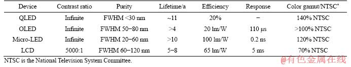
To conclude, LED-based display techniques hold many potential and intriguing properties, such as flexible, printable, wider viewing angle, wide operating temperature, color temperature tenability, high resolution, better contrast ratio, lower power consumption, transparent, and light weight, which have made them very convincing components in small or large size display field. The characterization of each display devices is listed in Table 1 [11-13].
2 OLED
Organic light-emitting devices or diodes (OLEDs) can convert electrical energy into light energy via electroluminescence (EL) by employing luminescent organic semiconductors. Typically, the OLED owns the advantages of flexible, ultrathin and transparent. Compared with the LCD, it has fewer processing steps and it is less component intensive than today��s LCDs, notably with the elimination of a backlight (OLEDs are self-emissive). Therefore, since their first commercialization in 1997, OLEDs have created considerable interest among scientists throughout the world and become an important component for third generation display and lighting technologies. The earliest type of OLED is fluorescent emitter, only employing singlet to generate the light. According to the spin-statics, only the 25 % singlet excitons created under electrical excitation contribute to the device electroluminescence, therefore the external quantum efficiency (EQE) is limited to 5 %. Luckily, the limitation was broken by the invention of the phosphorescent emitter, which use both the singlets and triplets to generate light. With the heavy metal atoms corporation, more triplets could be harvested with the enhanced intersystem crossing (ISC) process. Therefore, the phosphorescent emitter can reach the 100 % IQE theoretically. But the phosphorescent emitter remains a high cost with a use of heavy metal atoms, and efficiency roll-off occurs due to triplet-triplet annihilations at high current density [14]. Alternatively, in 2009, ADACHI group introduced a new type of OLED, based on thermally activated delayed fluorescent (TADF) materials. The TADF materials generally have a small energy gap between the S1 and T1 states and long lifetime of T1 states, which means the reverse intersystem crossing (RISC) process from T1 state to S1 state [15] could be completed by the thermal activation, bringing to delayed fluorescence. However, the singlet exciton transition dipole moment of the TADF materials is generally relatively small. As a result, the emissive lifetime can be 0.1�C1 ��s, which would cause a significant efficiency roll-off under high voltage. The energy transfer process happened in OLED of the whole three-generation OLED is briefly depicted in Figure 1 [16].
Table1 Characterization of LED based display devices [11-13]
Although different types of OLED have different working principles, the device architectures are similar. Modern OLEDs consist of a thin organic emitting layer sandwiched between an electron transport layer (ETL) and an organic hole transport layer (HTL) chosen to facilitate injection of each carrier into the emissive organic layer. The current OLED displays have an infinite contrast ratio, a faster response time, and an ultrathin and flexible outlook which could be used in the future wearable application. However, the conventional OLED has a short lifespan, and the burn-in is as a result of the intrinsic poor stability of organic molecular. The short operation life could be improved by the proper fabrication process, rational organic emissive molecular design and CTL engineering. Here, recent efforts on improving the performance of the OLED through the adjustment of the OLED device structure are presented.
2.1 Conventional structure improvement
The first OLED only has monolayer architecture, in accordance with efficiency output of OLED, more layers have been added with specialized function like hole injecting layer, hole-transporting layer, hole-blocking layer, and electron transporting layer. The extra layers are meant to overcome problems in two main processes in OLED: charge transfer and energy transfer. A good charge transfer should meet the following standards: facilitation of the charge injection, a balance of holes and electrons. And the energy transfer is supposed to harvest more excitons to generate light with high efficiency. The approaches to improve these two problems through device architecture regulation would be discussed in the following parts.
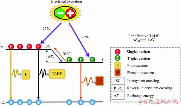
Figure 1 Singlet and triplet excitons radiation phenomena in OLEDs [16]
2.1.1 Charge transfer layer
The hole mobility of the HTL materials is two to three orders of magnitude higher than the electron mobility of several typical electron transporting materials. As a result, OLED always suffers from excess hole injection contrary to the QLED. The excess holes induce the reduction of current efficiency, non-radiative recombination of the excitons, and destruction of the emitting layer. With an aim of charge balance, a reduction of holes injection (hole blocking layer) or a facilitation of electrons (electron injection layer) is introduced to the device. The electron injection layer is utilized without changing device architecture. For example, a facile electron-injection architecture featuring a silver nanoparticle (AgNPs) interlayer-modified sol-gel-derived transparent zinc oxide (ZnO) ultrathin film is proposed (Figure 2(a)) [17]. The optimized EQE of the phosphorescent OLEDs 21.2% is at a current density of 20 mA/cm2. The main mechanisms of the efficient electron injection are: low energy barrier of between the ETL and organic layer, high electron mobility of the ETL. Therefore, by carefully selecting the charge transfer materials, excess holes would be recombined [17-23]. Besides increasing the amount of electron injection, a hole reduction strategy is always considered by the researchers. A typical HBL should process a wide energy band-gap, a deep HOMO energy level and the LUMO should be closely aligned with that of the ETL(Figure 2(b)) [23-28]. Other layers to regulate the charge injection, including the hole injection layer (HIL) and electron blocking layer (EBL), have been also proposed. Multilayer structure could bring a better performance but with a complexed fabrication, which is a trade-off.
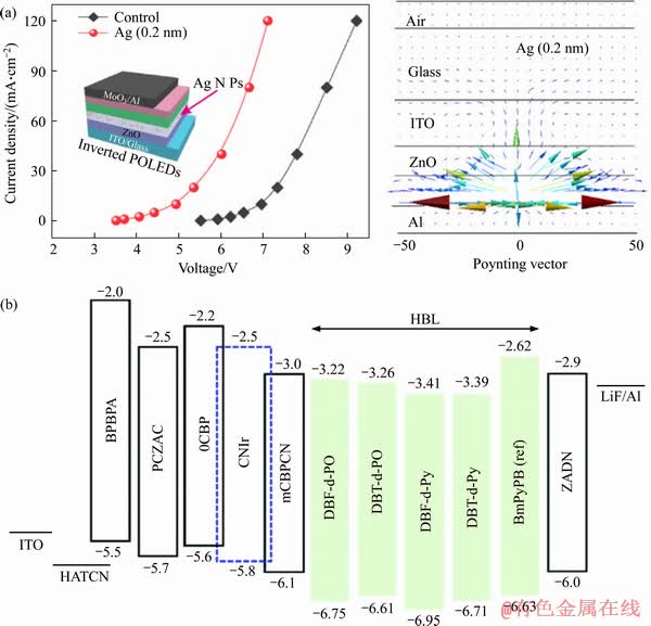
Figure 2 Electron-injection architecture and performance of an inverted phosphorescent OLED (a) and energy level (unit: eV) diagrams of blue OLEDs [27] (b)
2.1.2 Energy transfer
There are several energy transfer routes in a common OLED, which are considered as a double-edged sword. They may contribute to light emitting in a specific type of OLED, but could also be the cause of efficiency degradation in other types of OLED. By molecular design and device adjustment, different energy transfer mechanisms can be utilized to achieve high performance OLED. Increasing the luminance efficiency is a two-step process: harvest excitons as many as possible, and transfer the obtained excitons into desired photons as many as possible. The main focus is on the transfer to the obtained excitons. The type of the excitons that used to generate light divides the type of the emitter.
Researchers have widely accepted that effective exciton generation plays a crucial role in the realization of high efficiencies in OLEDs [16]. The excitons used to generate lights are two kinds: singlets for fluorescence, and triplets for phosphorescence. According to the spin statics, the singlets and triplets are generated by random charge recombination in the ratio of 1:3. Therefore, the fluorescence emitters have intrinsic low efficiency, as for the phosphorescence emitter, the theoretical efficiency is 75%, either. Luckily, the singlets and triplets could be obtained by transforming in many ways. Both singlets and triplet could be generated by the recombination of holes and electrons. Singlet can be transferred by triplet through triplet-triplet annihilation (TTA) and reverse intersystem crossing (RISC). As for triplets, they can be transferred by the singlets through intersystem crossing (ISC). Besides these conventional methods, there are many other methods to achieve the conversion of different states: exciplex formation [29, 30], intermolecular triplet to singlet energy transfer from the host to guest, and a high singlet-to-triplet cross-section ratio in conjugated small molecules and polymers [31], which mainly depends on the molecular design, so it will not be discussed in this review.
1) Singlets transfer
The transfer route is mainly based on two mechanisms: TTA and RISC. TTA is also known as triplet-triplet fusion, forming a singlet with an annihilation of two triplets. Therefore, the fluorescent emitter based on TTA has a theoretical IQE of 62.5%, corresponding to an EQE of 12.5% in the ideal case. As the maximum EQE is still low, this process is not popular.
Compared with TTA, RISC could greatly increase the IQE up to 100 % theoretically. The current fluorescent emitter based on efficient RISC is known as TADF. As mentioned above, the TADF has a small energy gap between the S1 and T1 states, which is typically less than 0.37 eV. Therefore, the RISC can be easily achieved by the heat activation. TADF emitter is typically composed of a double-dopant system: a wide-energy-gap host, a TADF-assistant dopant and a fluorescent emitter dopant. The host is meant to capture the excitons and transfer to the TADF dopants, then the desired singlets will be generated on the TADF dopants through RISC, finally the singlets are transferred to the fluorescent emitter dopant to generate light.
TADF has a theoretical 100 % IQE compared with conventional fluorescent emitter, and it has no heavy metal atoms, which is more environmentally friendly and cheaper when compared with phosphorescent emitter. However, it always suffers from short material life time, which is a major obstacle to the development of economically feasible, highly efficient, and durable devices for commercial applications. To fix this problem and improve the performance of the device, many methods have been proposed, but the device design has little effect on it. Instead, researchers concentrate more on the molecule design to get a better operation stability. The TADF emitters need to be designed to separate the highest occupied molecular orbital (HOMO) and the lowest unoccupied molecular orbital (LUMO) for small singlet-triplet energy gap and weakly overlapped HOMO and LUMO for efficient light emission [32]. The former condition is desired for efficient RISC and the latter condition is required for high photoluminescence quantum yield [33]. The TADF emitters have donor�Cacceptor groups with steric hindrance incorporated between them to form intramolecular excited states. Therefore, bond connection between donor and acceptor has a great influence on the charge transfer between donor and acceptor, such as introducing steric hindrance into the molecule. According to these molecular principles, many TADF devices with excellent performance have been proposed [34-37].
Although TADF combines the merits of fluorescent emitter and phosphorescent emitter, it still has too many problems, such as the complexed structure which induces the reliability problems. Luckily, the latest research presented a one layer sandwiched device structure, which achieved an EQE of 19% at 500 cd/m2, with 1880 h lifetime for an initial luminance of 1000 cd/m2 as displayed in Figure 3 [36]. Although there is still a long road before it comes to market, the simplicity of the structure might accelerate its development.
2) Triplets transfer
Triplets have an intrinsic theoretical high yield ratio of 75%. As the demand of more triplets in phosphorescent emitter, the ISC is preferred to transfer the singlets to triplets. Coupled with the heavy metal atoms, an efficient ISC process would be promoted due to a strong spin-orbit coupling effect. Therefore, strong phosphorescence would be achieved in the room temperature with the 100 % EQE theoretically.
The phosphorescence device structure is mainly the same as fluorescent emitter, but the emitting layer contains host materials. Due to the long phosphorescent time, the emitters are usually doped into the host material at low concentration not only to suppress the TTA and concentration quenching effects [38, 39], but also harvest more excitons, transferring to emitter to generate phosphorescence. Therefore, the host engineering is supposed to be as important as the emitter. Conventional methods to improve the efficiency of the phosphorescent emitter are: modifying the functional unit of the host material to adjust the electronic properties [40] and regulating the configuration of the emitting molecular, such as small molecular [41, 42], dendrimers [43] and polymers [44, 45].
Although the phosphorescent emitter owns the good efficiency, the high cost hinders the prospective application of these devices in many fields, including mobile displays, large-screen displays, and general lighting. Therefore, the heavy metal atoms need to be replaced.
2.2 Excitons confinement
The excitons should be confined in the emitting layer to complete light emitting. Similar to the charge, the confinement of excitons is required in the emissive layer to increase exciton density, so that these excitons can effectively transfer the energy to stimulate the light emitting molecule to a major extent resulting in high device efficiency. The confinement is always completed by charge block layer, as a result of a large energy gap within the emissive layer. As for the phosphorescent OLEDs, an effective exciton confinement within the emissive layer can also be realized by employing high triplet energy host materials, which is detailedly reviewed by WONG��s group in 2015 [40]. Layers are introduced into the device to improve the performance, charge injection layers and charge blocking layers are inserted to confine the recombination zone in the emitter layers, suppressing the confinement of excitons. But it also increases the cost of complex fabrication and operation risk.
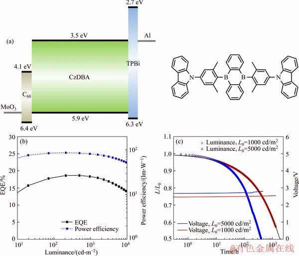
Figure 3 Device layout and molecular structure of TADF emitter CzDBA (a), EQE and power efficiency as a function of luminance (b) and operational lifetime of single-layer CzDBA OLEDs [36] (c)
2.3 New architecture
Besides the conventional structure of the OLED, there are also other architectures. The p-i-n structure was introduced by HUANG et al [46] to overcome the limitation of voltage drop due to high resistivity of comprising semiconducting layers in a device which decreases the overall efficiency of the device. With an intrinsic emitting layer (i) sandwiched by p-doped (p) and n-doped (n) transport layer, p-i-n structure has a relatively low driving voltage and high substrate compatibility, while maintaining high power efficiency and long lifetime.
In addition, tandem OLED, that has two or more electroluminescence (EL) units connected electrically in series with unique intermediate connectors within the device (Figure 4), has been studied to construct high-efficiency, high-luminance, and long-lifetime OLED displays [47-49]. Researchers have found that the current efficiency of a tandem OLED containing NEL units (N>1) should be N times that of a conventional OLED containing only a single EL unit. In this new structure, the double or more EL layers were suggested to confine the charge carriers to a region near the hole transporting and emissive layer interface, while mixed-emissive layer design has a large interfacial area between the hole transporting layer and the emissive layer to facilitate exciton formation [50, 51]. Different with the monochromatic tandem OLED that used for small- size displays, white tandem OLED are usually adopted by the large-size displays, which need the mixture of two or more separated devices with complementary colors, such as orange-blue, and red-green-blue emitters to cover the whole visible region as much as possible [52, 53]. In addition, white tandem OLED can also be achieved using the structure of tandem OLED with a set of electrically connected EL units in the single device [54].
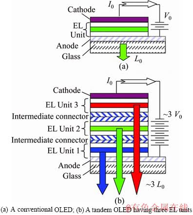
Figure 4 Schematic of OLEDs [47]:
2.4 Future and conclusions
OLED has already been successfully utilized in many applications. But the blue OLED still needs a lot of development. As blue emitter is essential to the OLED based display, the TADF received a lot of attention as it could lead to an efficient and long-lasting blue OLED emitter. Some companies (Kyulux, Cynora, Idemitsu Kosan) announced that the efficient commercialized TADF emitter have been presented [55]. In October 2019, Samsung announced that it is going to invest $10.8 billion to establish QD-OLED TV production line, which is based on the efficient blue OLEDs. The huge investment from Samsung and LG Display would accelerate the application of OLED.
To sum up, there are three main kinds of OLED currently, and MATSUMOTO et al [56] have proposed the next-generation of OLEDs in which TADF emitters are utilized as sensitizers of fluorescent dye molecules. Fluorescent emitter has its low theoretical efficiency, phosphorescent emitter with heavy metal atoms assisted is expensive, TADF emitter is less stable than the previous types. But the OLED is still the leading techniques in the market with its rapid development. According to the IHS Markit, the active matrix OLED (AMOLED) demand in smartphone raises to the highest record in the third-quarter 2019, following the increased demand for AMOLED displays, Samsung Display regained its leading position in the market (with a 29% market share), replacing BOE (19%). The third largest suppler is Tianma (13%) [57]. The market share of OLED continues increasing steadily, with the constantly huge investment in OLED, the obstacles would be overcome gradually.
3 QLED
Quantum Dots (QDs) are nanoscale semiconducting crystals that have unique optical and electronic properties due to quirks of quantum mechanics. The energy gap of the QDs can be simply tuned by the size, regardless of the properties of the consisting materials. Therefore, the band gap could be tuned simply. Owing to their properties of tunable emission wavelength, high color purity, high photoluminescence (PL) quantum yield, good stability and cost-effective fabrication, scientists have found many applications for them in optical devices since 1980s. It is firstly used as a color filter to improve the light quality of other emission techniques, which is known as the first and second generation of quantum dots display. The first generation of QDs display was used into the LCD field, as the enhanced backlight, which would be discussed later. The second-generation QD display uses a QD color filter with blue OLED. To conclude, the first and second QLEDs are based on the photoluminescence, utilizing the wide color gamut of the QD.
However, the QD phosphors which are used in display devices are not self-emissive, which means they need to be replaced by QD light-emitting diodes in order to be competitively efficient. Therefore, to best take advantages of the perfect emission ability, scientists began to study the self-luminous device known as the third generation of quantum dots display, which is based on the electroluminescence [58].
The advantages and shortages are quite the same. With the merits of flexible, high resolution, and perfect purity, the concept of the e-skin, smart-fiber and other high-end electronic devices could be out of the lab and gets commercialization. There are also many obstacles needed to be overcome, such as the charge imbalance, weak resistance of the water, non-radiative Auger recombination. Fortunately, these shortages can be minimized with the regulation of not only device structure but also the QDs fabrication.
The traditional third generation QLED device structure takes an example of the OLED structure, modern QLEDs consist a thin QD layer sandwiched between an ETL and a HTL chosen to facilitate injection of each carrier into the emissive QD layer [59]. Some QLED also has a charge injection layer (CIL) to enhance the carrier injection. Herein, we present a summary of the high-performance QLED achieved by the device structure design.
3.1 Conventional structure improvement
The typical device structure is consisted by 5 parts. Besides the emitting layer, the charge layer plays the critical role in the regulation of the whole device performance.
The charge transport layer used in QLED is supposed to achieve electron and hole injection efficiently and evenly. With a careful design of the CTL material, the precise energy band cascade of the electrode and emitting layer would be completed. As a result, an efficient charge injection into emitting layer and powerful confinement of the exciton would be achieved. As for the electrodes, they have more influence on the stability instead of the luminance performance. Therefore, without changing the device architecture, improving each part of the QLED device component would gain a huge improvement of the performance with a synergetic effect.
3.1.1 Charge transport layer
Charge transport layers are meant to facilitate the carrier injection with high efficiency and charge balance. The charge balance is always inevitable, as a result of different mobility and transport energy barriers of holes and electrons. The surplus carriers have many negative effects to the device: Auger non-radioactive recombination [60], device destruction, exciton delocalization, and parasitic radiation. Finally, color purity, luminance efficiency and lifespan are degraded greatly. Therefore, many efforts have been involved to avoid these unpleasant effects. In most cases, the electron injection is much more efficient in QLED, which would induce an electron leakage current. There are commonly four typical methods to reduce the built-up electron injection: selecting a smaller HOMO material as HTL [61], decorating the QD with a shell to block the charge injection, combining the QD layer and HTL [62-65], and inserting a proper insulating layer between the QD and ETL [66].
Since the EQE is a measurement of the number of charges that radioactively recombine in the QD layer, it is highly sensitive to the degree of charge balance in the QLED. In the past three years, many strategies have been inserted to achieve a high EQE with a well balance of charge. The reduction of the defect density with the tunable annealing time of the ETL materials has received a good EQE of 10%, causing the enhanced electron mobility, overall current and luminance [47].
3.1.2 Exciton confinement
With a large energy barrier between QD layer and CTL, the excitons are confined in the emitting layer, sandwiched by the charge transport layers. If the exciton delocalization occurs, the photons emitted by the device would have a wide energy distribution, resulting an efficiency degradation. Besides, the degradation of the device lifespan will also happen. Many strategies have been proposed to improve this situation. QD shell-core structure is used to protect the vulnerable core. With a careful design of the shell of the quantum dots, the shell with ligands on it would confine the excitons in the emitting layer. As for the device structure design, it is always based on the regulation and adjustment of the layers inserted in device.
3.2 Other layers inserted
To achieve a better charge balance and excitons confinement to get a better performance, the extra layers are proposed. Such as the charge injection layer and charge block layer. With a proper alignment of these layers, a better performance would come true at a cost of a more complex fabricating process.
3.2.1 Interface modification
At the interface of ETL/QD, excitons are easily quenched by an interfacial charge transfer process and/or by an intragap-assisted non-radiative recombination process [67, 68]. And the electron injection always overwhelms the hole, so the possibility of the non-radiative recombination would increase, degrading the efficiency and lifespan. With the modification of the interface, a suppression of the non-radiative process and electron injection would be achieved. With 13 nm Zn0.85Mg0.15O interlayer inserted as an interface modification layer, improved efficiency of red and green devices was achieved (Figures 5(a)-(c)) [69]. The Mg-doped ZnO exhibits a decreased electron mobility and a higher conduction band maximum, therefore, an efficient charge balance was achieved with a reduction of the electron injection. SHEN et al [70] for another example, used double Al2O3 interlayers as interfacial modifiers on both sides of EML (ETL/Al2O3/EML/Al2O3/HTL), resulting in an increase of the current efficiency from 11.3 to 15.3 cd/A. With an ultrathin insulating PVK layer used to modify the interface between the ZnO nanoparticals and QDs (Figure 5(d)), the inverted QLED outpaced the EQE of the conventional device for the first time with an EQE of 22.4% [71].
3.2.2 Insulating layer
With an insulating layer utilized between the ETL and QDs, the electron injection would be achieved. In 2014, with the insertion of a poly (methyl methacrylate) (PMMA) insulating layer (~6 nm) between the QDs layer and the ETL, JI et al [72] have achieved a red QLED with the best EQE of 20.4 % and a long life. Although their work was followed by many other groups, the precise thickness control of the insulator limits its application. Polyethylenimine (PEI) has also been used as the electron blocking layer with utilization of its intrinsic insulator property. With the adjustment of the thickness, a maximum EQE of 16.1% was achieved with the thickness of 15 nm. There is other insulating layer inserted in the QLED to regulate the electron injection, such as PFN, CsCO3 doped AZO, and PEI [71], with precise thickness control, a balanced charge injection would be completed.
3.3 Inverted structure
Inverted structure is useful for active-matrix (AM) OLED and QLEDs with n-channel thin-film transistors (TFTs) such as oxide TFTs. An inverted device structure rather than the conventional structure is preferred for future QLEDs, because the transparent indium tin oxide (ITO) as the bottom cathode can be directly connected to an n-type thin film transistor (TFT), which is generally faster than p-type TFT [73], allowing the direct programming of the TFT gate-source voltage independent of the electrical characteristics of QLEDs.
The inverted structure processes the fabrication advantages, which reduces the cost and improves the efficiency [74, 75]. Furthermore, unlike the conventional structure, the first spin-cast layer of ZnO nanoparticles (NPs) can go through high temperature annealing without damaging other layers, as demonstrated in Figure 6. With regard to fabrication, solution processing is preferred because of its cost-efficiency and easy process ability [74, 75]. Therefore, the inverted QLEDs that are fabricated solely by solution processing are preferred by numerous groups since it was firstly proposed by KAWK et al [60] in 2012. Generally speaking, current QLED devices with high performance and stability are generally inverted structure, owing to its easy fabrication process and good hole injection [60, 76, 77].
Figure 5 Schematic structure (a) and energy level alignment (b) of inverted QLED with a ZnMgO modification layer, normalized EL spectrum of device [69] (c) and flat-band energy level diagram of an inverted QLED with sandwich-structured quantum-dot layer [71] (d)
3.4 Future and conclusions
The stability of QLED is the issue that needs to be overcome because the QLED suffers the sensitive damage from moisture and oxygen. To address this problem, enhancing the stability of QDs is the first choice as the QDs are usually not stable when exposed in oxygen, water, thermal heating and UV illumination. Shell design, ligand design, and overcoating have been proposed to improve the stability of QDs [78-80]. Encapsulation of QDs by polymer matrix is also an efficient way to protect the QD films [81, 82]. Stability enhancement of QLED can also be achieved by controlling the HTL. Various metal oxides, such as MoOx, WOx, NiO and VOx, have been adopted in the HTL to prevent the penetration of water and oxygen [83-85]. Finally, by controlling the ETL, the lifetime of QLED can also be remarkably enhanced [86, 87]. For example, by introducing an ultrathin PMMA layer between the ZnO and QD layers, the electron injection was delayed, which greatly improves the lifetime of the as-fabricated QLED from 5000 to 100000 h at a brightness of 100 cd/m2 [88].
At the same time, as the newly-developing market requirement of the flexible display, such as smart watch, foldable mobile and e-skin, the standard of the electrodes also increases. As for the application in wearable device, qualified electrodes should be transparent, flexible, compatible to the substrate and most importantly, powerful protection of the moisture and oxygen, which is essential to prolong the lifetime of QLED, but few attentions are put on this field. On the other hand, the toxicity of QLED is also a big problem. Cd-based QLED has the wonderful and reliable performance, it is not so surprising as the 20 % EQE of Cd-based QLED has a long lifetime [89, 90]. Although the high EQE is always with a low luminance and vice versa, the relatively low luminance (<2000 cd/m2) is enough to satisfy the standard of regular electron device (e.g. laptop, and mobile phone), which is commonly on the order of 100. What is the most important is the intrinsic toxicity of Cd-based QDs, which limits its commercialization. Therefore, improvement of the non-toxic quantum dots receives more and more attention.
InP and perovskite based QDs are the hot spot in this field. According to the latest research from Samsung Advanced Institute of Technology, as shown in Figure 7, the InP/ZnSe/ZnS QLED device achieves a maximum EQE of 21.4 %, with a 107 h of operation life at 100 cd/m2 [91]. The RGB color emitter with great purity, cost efficient fabrication and excellent lifetime is supposed to be the big step for the commercialization of QLED. Big companies like Samsung, Hisense, TCL and BOE have been working together with start-up companies (e.g. Najing Tech, QD vision and Nanosys) in the QD field to produce advanced display device. Samsung Display has set a target to mass-produce QD-OLED displays by 2021.
Figure 6 Device schematic (a) and cross-sectional TEM image (b) of a solution-processed, multilayered white QLED [69]
4 Micro-LED
Micro-LED (also known as mLED or ��LED) is a display technology based on tiny (<100 ��m) LED devices that are used to directly create color pixels. The average LED chip including substrates and epi-wafer layers measures about 100 to 500 ��m. Micro-LED displays have the potential to create highly efficient and flexible displays, such as wearable devices with its small size, higher yield rates and high brightness in outdoor environments compared to OLEDs. Additionally, it shows low energy consumption. Therefore, it has the potential to challenge the current high-end OLED displays.
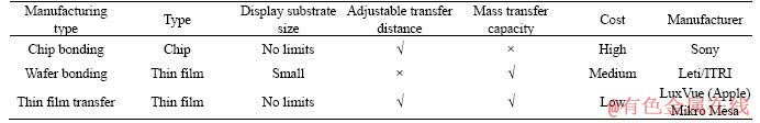
Micro-LED designs are widely classified into two types: chip-based micro-LEDs (transferring packaged red-green-blue unit) and thin-film micro-LEDs (having thickness less than 5 ��m). The main differences are concluded in Table 2 [92].
The micro-LED with chip-based transfer is already on the verge of commercialization by successfully transferring millions of tiny LED pixels in a display panel [93, 94]. Besides the performance improvement of the micro-LED, researches are focusing on the transfer methods. Current technologies do not satisfy the standards of low-cost and high-speed fabrication, as the chip- based micro-LED needs a million of individual chip transfer. Instead, a possible solution comes from thin-film based micro-LEDs, which can increase transfer speed by using cost-effective, fast, and massive transfer in one time. In addition, the laser lift-off process with flip-chip bond has also been used to transfer of the ��-LED chips with 49152 pixels onto the TFT backplane, which demonstrates a 2 in (1 in=2.54 cm). LED displays with excellent gray scale image [95]. As the micro-LED is mostly based on the previous mature LED technologies, the device structure and working mechanism are much simpler and more mature than the OLED and QLED. The aim of the structure design is meant to dissipate heat, decrease the forward voltage, and extract more light from the device, instead of regulating the energy band or increasing charge injection in QLED and OLED.
4.1 Resistance reduction
The characteristic of micro-LEDs is size- dependent, which was first mentioned by JIN et al [96] in 2001. In 2012, TIAN et al [97] revealed that higher current density at the same applied voltage, less efficiency droop, less maximum EQE dropped would be achieved as the device shrinks [97]. Size reduction is also an easy way to improve the performance with a lower forward voltage, higher irradiation density, and a better current efficiency,as the resistance of the micro-LED is easily influenced by the size reduction [98-102].
Figure 7 Illustration and cross-sectional TEM image of QD-LED device structure (a), current density and luminance versus voltage profiles (b), EQE-luminance profile (c) and lifetime measurement of QD-LED [91] (d)
Table 2 Differences of manufacturing for micro-LED designs [92]
There are other ways to reduce the resistance, a current spreading layer is introduced by metal ohmic contact [103, 104], annealing process, and modulation of doping concentration [105]. KIM et al [106] demonstrated that the EQE can be improved by replacing indium-tin oxide (ITO) with tunnel junction grown by metal-organic chemical vapor deposition (MOCVD) as the current spreading layer. The EQE of the device increases from 25% to at least 30.6% as a result of more uniform current spreading and better optical transparency of tunnel junction. KONOPLEV et al [107] showed that the current density distributed uniformly in the active region of the 30 ��m device, whereas strong current crowding was observed at the metal contact for a 300 ��m device (Figure 8). As a result, the 30 ��m device has an average temperature higher than the smaller one. Therefore, a better heat dissipation and current spreading could be achieved with the size reduction of device.
4.2 Other methods
However, as the size reduces, the effect of sidewall damage and surface recombination induced by dry etching mesa could not be neglected any more [107-109]. It was revealed that smaller micro-LEDs yield greater surface recombination loss [83, 110-113]. To avoid this trend, sidewall passivation using dielectric materials has been utilized as a conventional method to suppress the above mentioned problems. Plasma-enhanced chemical vapor deposition (PECVD) and atom-layer deposition (ALD) are inserted to deposit a dielectric confinement layer on the surface. CHEN et al [114] presented the leakage current was reduced by two orders of magnitude, and the light output increased by 115% with SiO2 PECVD. The light output power of devices with PECVD passivation was remarkably lower than that of devices with ALD passivation and without passivation since the PECVD reduces the transparency of ITO greatly. Although ALD sidewall passivation suppresses the surface recombination and sidewall defects, it does not remove plasma damage from dry etching. Therefore, more methods are needed to recover the surface damage with ALD.
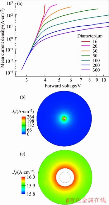
Figure 8 Current density-voltage characteristics of LEDs with various outer diameters (a), distributions of current density in active region of LED with diameter of 300 ��m at 10 mA (b) and 0.1 mA [107] (c)
In addition, for the integrated ��LEDs, an additional bond stack is typically required, but it could create a lower limit on the pixel size [115]. With further reducing the pixel dimensions for ��LED matrix display, the use of a bond stack should be avoided to achieve high pixel size of the ��LED matrix on CMOS circuits. To this end, the heterogeneous integration of the ��LED matrix display based on GaN on top of the CMOS driver-integrated circuit (IC) is reported without employing a dedicated bond stack [116]. In this report, using the copper pillar process, a ��LED display driver IC, with a compact size of 3 mm��4.4 mm, has been designed, implemented, and verified experimentally for ��LED matrices with individual ��LED pixel diameters of 20 and 50 ��m, respectively.
Besides the fabrication, to achieve a higher EQE with extracting more light from the device, many other methods are inserted, such as patterned sapphire substrate, lens integration, surface texturing, and Bragg reflector implementation [117, 118].
4.3 Future and conclusions
As for the commercialization of the full-color display of micro-LED, two main strategies are considered: 1) color conversion from blue/UV ��LEDs using quantum dots and 2) transfer of red, green and blue ��LEDs in three separate processes.
Compared to OLEDs, micro-LEDs promise to be much more efficient, brighter, more durable and with a higher color gamut. Micro-LEDs are based on well-established LED devices, which means that it could potentially be a technology that is relatively easy to scale up.
According to the research and markets, a market research institution, the global micro-LED display market is predicted to soar from USD 0.6 billion in 2019 to USD 20.5 billion in 2025, with a compound annual growth rate of about 80% [119]. According to EVEN��s [120] optimistic estimate, the market of micro-LED display will reach 330 million units by 2025. To conclude, progress in cost reduction and assembly techniques and the potential for new modes of operation position micro LED technology would be the motivation for the micro LED development in the next few years.
5 LCD
Liquid-crystal display (LCD) is a flat-panel display or other electronically modulated optical device that uses the light-modulating properties of liquid crystals combined with polarizers. Being developed for several decades, the LCD has been successfully commercialized, the cost of it has been decreased to the lowest among the current display device. From watches and camera screen to large scale television and giant screens, it has been used widely, but the intrinsic shortages of the LCD grow significantly at the same time. Such as the slow response time, poor view angle, low contrast ratio and narrow color gamut, which are criticized by costumers repeatedly and limit the further development of LCD. Producers begin to utilize other materials or design to improve the performance of LCD.
5.1 Backlight enhancement
Declining size of LED backlight unit is supposed to be efficient to improve the HDR display, as the Mini-LED (chip size below 200 ��m) used in LCD backlight has been proved to be beneficial to the photograph quality. And this method has been applied in the current advanced display device widely. In 2019 Display week, Tianma presented LTPS LCD smartphone display based on the Mini LED backlight, which features over 100000:1 contrast ratio, over 1000 nits brightness, high color gamut and wide viewing angles. CSOT also showed a 5.99 inch LTPS display (1080��2160 resolution), 500 nits brightness, over 100000:1 contrast ratio with mini-LED backlight, an ultra slim mini-LED 15.6-inch notebook based on LTPS TFT, 3840��2160 resolution, 1000 nits brightness, 20000:1 contrast ratio and NTSC 100 % color gamut. BOE exhibited HDR notebook featuring 15.6 inch oxide display and mini-LED backlight with very high refresh rate of 240 Hz [121]. With the newly developed backlight techniques, the enhanced LCD techniques still has the potential to maintain the dominate position in market with its mature market chain and low price.
5.2 Color filter
Building a narrow emission band color filter is one option that can be used to enlarge the color gamut. Common color filters are phosphors and QDs, but the QDs has become more popular than the phosphors as the material science developed. The QD enhanced films can absorb blue light and emits green and red light with narrow bandwidth, as a result, the color gamut of LCD can be improved to >100% of the NTSC color triangle [122, 123]. In addition, due to the narrow emission bandwidth of QD, the optical efficiency can also be improved because QD enhanced films can match the backlight spectrum ideally to the color filter bandwidths [124]. For LCDs using conventional phosphors, the color gamut is ~72% of the NTSC standard. To further improve the color gamut, RbNa(Li3SiO4)2: Eu2+ phosphor was adopt, which realizes a wide color gamut (113%) and high luminous efficacy (111.08 lm/W) for a white LED [125]. As for the LCDs enhanced by QDs, the color gamut of the LCDs can be improved to larger than 110% of the NTSC standard [126], which outperforms not only the conventional phosphors used as down-converter of LCD, but also the displays based on OLED. However, its optical efficiency is always compromised [127]. Therefore, besides improving the current enhanced techniques, other new methods are urgently needed [128].
5.3 Future and conclusion
The LCD techniques have been developed for a long time, but the intrinsic problems are still too stubborn to overcome. In recent years, the improvement of the performance is mainly based on the development of backlight technology and QDs. With the rapid development of OLED and micro-LED, low price will not be the motivation for consumers to buy LCD display device. It is forecasted that the LCD TV panel shipments are expected to decline in 2020, falling by 7% to total 265 million by various reasons according to IHS Markit [129]. And the LG Display, Panasonic and BOE declared that the investment in the LCD would be decreased, as a result of oversupply and maturation of the market, according to the LEDINSIDE��s report [130]. But it is still optimistic that improvements in contrast and color performance with the advanced backlight technology and wide color gamut technologies used in the LEDs for backlights will continue to impress advertiser in LCD market, with an affordable price in the next few years.
6 Future of display field
Cost becomes the biggest problem when device goes to mass production among the QLED, OLED and micro-LED. Various layers used in the OLED and QLED are fabricated by the solution process and vacuum evaporation process. The process with high temperature, inert gas protection, and localized injection operation offers a better performance with a high cost needed, which are severely against applications. On the other hand, the solution process approach proves to be more efficient by the use of methods like coating or printing which are highly cost-effective, feasible for mass manufacturing, and promising for large area displays, although it has several drawbacks: the solubility of some organic materials in various organic solvents, undesired blending of two layers during subsequent coatings, and the resultant morphological and compositional defects in layers [131]. As mentioned above, the large-scale commercial application of state-of-art QLED and OLED has not been available yet. Fortunately, numerous efforts have been devoted into the all solution fabrication process, which is essential for the large-scale production with an acceptable cost of time and money. As for micro-LED, researchers focus on the transfer method of the pixel. Currently, transferring millions of LED still remains the biggest problem of micro-LED. ACF mass transfer method induces a strong adhesion between the micro-LED chips and the electrodes, therefore, the electronic and optical characteristic was remained [132]. PDMS stamp has also been used to transfer micro-LED with large scale, high yield and good efficiency [133, 134].
Display technique is born to change human��s life, so it depends on the market environment. The flat panel display demand will continue to grow in 2020, mainly driven by migration to larger displays for major applications, such as TVs, desktop monitors, mobile PCs and smartphones, but the pace is expected to slow through 2021. Great investment in panel factories in China pushes the display techniques evolve, but it is also expected to continue to cause oversupply next year. As the market forecast for both demand and supply does not seem so optimistic, producers and set makers have been trying to develop more advanced products and technologies, such as 8 K resolution for TVs, QLED and OLED TVs and foldable displays for smartphones and tablet PCs, to support the growing consumer demand.
Besides, the display techniques also inspire the development of techniques in other fields. The improving performance of the current display device would lead to the larger storage of the videos and photos, so the date transportation would cause a larger amount of time. Therefore, a more efficient date transportation strategy is needed as the 5G communication is around the corner. Besides, the photo quality of the original data should be enhanced with a faster speed than the development of the display field, or the better display technology would not be useful as we expect.
7 Conclusions
1) As the growth of consumers�� demand and development of the techniques, future display device requires high quality pictures display, flexibility and lightweight, and the LED-based display has the potential to achieve the goal. However, each type of the LED display has its own disadvantages.
2) We present the development of the display devices and the improvement of the devices through the structure adjustment. Several obstacles of each LED-based device and corresponding solutions are demonstrated.
3) This review also offers a outlook of current situation of the progress of commercialization and market environment. Giant companies (Sony,Apple, etc.) keep increasing the investment in micro LED, Samsung��s latest research marked the significant step for the QLED to come to the market, the OLED and LCD display devices are constantly improved with lower price and better quality by many companies. With both the scientists in lab and companies�� effort, the obstacles of the previous techniques would be overcome, and new advanced techniques will come up constantly.
References
[1] HOWSTUFFWORKS. How OLEDs work[EB/OL]. [2018-04-22]. https://electronics.howstuffworks.com/oled3. htm.
[2] BELLIS M. Television history and the cathode ray tube [EB/ OL]. [2017-04-06]. https://www.thoughtco.com/television- history-cathode-ray-tube-1991459.
[3] VICKERY R C. Van Nostrand��s scientific encyclopedia [M]. Germany: John Wiley & Sons Inc, 2005.
[4] COUSOULIS M. Handbook of digital imaging [M]. Germany: John Wiley & Sons, Inc, 2015.
[5] BAGHER A M, VAHID M M A, MOHSEN M. A review of challenges in display technology [J]. International Journal of Electrical Components and Energy Conversion, 2017, 3(2): 26-39. DOI: 10.11648/j.ijecec.20170302.12.
[6] LIU J, CHEN C T, CHEN C H. Introduction to organic light-emitting diode (OLED) [M]// Handbook of Digital Imaging. 2015. DOI: 10.1002/9781118798706.hdi022.
[7] DENG Peng, ZHANG Ke, CHAO V S, MO Wei-jing, LAU K M, LIU Zhao-jun. Full-color pixelated-addressable light emitting diode on transparent substrate (LEDoTS) micro-displays by CoB [J]. Journal of Display Technology, 2016, 12(7): 742-746. DOI: 10.1109/JDT.2016.2518491.
[8] GUO Wei-jie, CHEN Nan, LU Hao, SU Chang-wen, LIN Yue, CHEN Guo-long, LU Yi-jun, ZHENG Li-li, PENG Zhang-bao, KUO Hao-chung, LIN Chih-hao, WU Ting-zhu, CHEN Zhong. The impact of luminous properties of red, green, and blue mini-LEDs on the color gamut [J]. IEEE Transactions on Electron Devices, 2019, 66(5): 2263-2268. DOI: 10.1109/TED.2019.2906321.
[9] KIM H, MISUN R, JAMES H J C, HYUNSOO K, TAK J, JIN J. Ten micrometer pixel, quantum dots color conversion layer for high resolution and full color active matrix micro-LED display [J]. Journal of the Society for Information Display, 2019, 27(6): 347-353. DOI: 10.1002/ jsid.782.
[10] SEKIGUCHI H, YUKIMASA H, KEISUKE Y, AKIHIRO W, HIROSHI O, KATSUMI K. Fabrication and optical properties of regularly arranged GaN-based nanocolumns on Si substrate [J]. Journal of Vacuum Science & Technology B: Microelectronics and Nanometer Structures, 2019, 37(3): 312-319. DOI: 10.1116/1.5088160.
[11] LEE H E, JUNG H S, JUNG H P, SEONG K H, SANG H P, SENG H L, JAE H L, ILSUK K, KEON J L. Micro light-emitting diodes for display and flexible biomedical applications [J]. Advanced Functional Materials, 2019, 29(24): 08075. DOI: 10.1002/adfm.2018 08075.
[12] YANG Y, ZHENG Y, CAO W, XUE J, HOLLOWAY P H, QIAN L, TITOV A, HYVONEN J, MANDERS J R. High- efficiency light-emitting devices based on quantum dots with tailored nanostructures [J]. Nat Photonics, 2015, 9(4): 259- 266. DOI: 10.1038/nphoton.2015.36.
[13] KIM J H, HAN C Y, LEE K H, AN K S, SONG W, KIM J, OH M S, DO Y R, YANG H. Performance improvement of quantum dot-light-emitting diodes enabled by an alloyed ZnMgO nanoparticle electron transport layer [J]. Chem Mater, 2015, 27(1): 197-204. DOI: 10.1021/cm503756q.
[14] HE G F, SCHNEIDER O, QIN D, ZHOU X, MARTIN P, LEO K. Very high-efficiency and low voltage phosphorescent organic light-emitting diodes based on a p-i-n junction [J]. Journal of Applied Physics, 2004, 95(10): 5773-5777. DOI: 10.1063/1.1702143.
[15] UOYAMA H, GOUSHI K, SHIZU K, NOMURA H, ADACHI C. Highly efficient organic light-emitting diodes from delayed fluorescence [J]. Nature, 2012, 492(13): 234-238. DOI: 10.1038/nature11687.
[16] JOU J H, KUMAR S, AGRAWAL A, LI T H, SAHOO S. Approaches for fabricating high efficiency organic light emitting diodes [J]. Journal of Materials Chemistry C, 2015, 3(14): 2974-3002. DOI:10.1039/c5tc90053k.
[17] ZHOU Lei, XIANG Heng-yang, ZHU Yu-fu, OU Qing-dong, WANG Qian-kun, DU Juan, HU Rui, HUANG Xian-bo, TANG Jian-xin. Multifunctional silver nanoparticles interlayer-modified ZnO as the electron-injection layer for efficient inverted organic light-emitting diodes [J]. ACS Applied Materials & Interfaces, 2019, 11: 9251-9258. DOI: 10. 1021/acsami. 8b21355.
[18] DING L, WANG J N, NI T, ZHANG F H. Low-voltage inverted organic light-emitting diodes with double-layer election injection layer based on silicon dioxide [J]. Applied Physics Letters, 2019, 115(8): 83301. DOI: 10.1063/1.5094 185.
[19] LEE H, MAENG M, HONG J, NAJNIN R, MOON J, CHO H, LEE J, YU B, PARK Y, CHO N S. Highly efficient green, blue, and white phosphorescent inverted organic light-emitting diodes by improving charge injection and balance [J]. Journal of Materials Chemistry C, 2017, 5: 9911-9919. DOI: 10.1039/ C7TC02795H.
[20] RAO G, WANG X, WANG Y, WANG Y P, YAN C, CHU J, XUE L, GONG C, HUANG J, XIONG J, LI Y R. Two- dimensional heterostructure promoted infrared photodetection devices [J]. InfoMat, 2019, 1: 272-288. DOI: 10.1002/inf2.12018.
[21] SHIN H, LEE J H, MOON C K, HUH J S, SIM B, KIM J J. Sky-blue phosphorescent OLEDs with 34.1% external quantum efficiency using a low refractive index electron transporting layer [J]. Advanced Materials, 2016, 28(24): 4920- 4925. DOI: 10.1002/adma.201506065.
[22] ZHANG J, YU Y, WANG P, LUO C, WU X, SUN Z, WANG J, HU W D, SHEN G. Characterization of atomic defects on the photoluminescence in two-dimensional materials using transmission electron microscope [J]. InfoMat, 2019, 1: 85-97. DOI: 10.1002/inf2.12002.
[23] ADAMOVICH V, CORDERO S, DJUROVICH P I, TAMAYO A, THOMPSON M E, DANDRADE B W, FORREST S R. New charge-carrier blocking materials for high efficiency OLEDs [J]. Organic Electronics, 2003, 4(2, 3): 77-87. DOI: 10.1016/j.orgel.2003.08.003.
[24] HUANG C J, KANG C C, LEE T C, CHEN W R, MEEN T H. Improving the color purity and efficiency of blue organic light-emitting diodes (BOLED) by adding hole-blocking layer [J]. Journal of Luminescence, 2009, 129(11): 1292- 1297. DOI: 10. 1016/j.jlumin.2009.06.019.
[25] JANG S, HAN S H, LEE J Y, LEE Y. Pyrimidine based hole-blocking materials with high triplet energy and glass transition temperature for blue phosphorescent OLEDs [J]. Synthetic Metals, 2018, 239: 43-50. DOI: 10.1016/ j.synthmet.2018.03.002.
[26] JANG S, LEE K H, LEE J Y, LEE Y. Dibenzo[b, d]furan and dibenzo[b,d]thiophene molecular dimers as hole blocking materials for high-efficiency and long-lived blue phosphorescent organic light-emitting diodes [J]. Journal of Materials Chemistry C, 2019, 7(31): 9599-9608. DOI: 10. 1039/C9TC02689D.
[27] JANG S, LEE K H. LEE J Y, LEE Y. Novel hole blocking materials based on 2,6-disubstituted dibenzo[b,d]furan and dibenzo[b,d]thiophene segments for high-performance blue phosphorescent organic light-emitting diodes [J]. Journal of Materials Chemistry C, 2019, 7(31): 826-834. DOI: 10.1039/c8tc04900a.
[28] ZHOU Liang, ZHANG Hong-jie, DENG Rui-ping, GUO Zhi-yong, FENG Jing, LI Zhe-feng. Electroluminescence of hole block material caused by electron accumulation and hole penetration [J]. The Journal of Physical Chemistry C, 2008, 112(38): 15065-15070. DOI: 10.1021/jp805088v.
[29] JANKUS V, CHIANG C J, DIAS F, MONKMAN A P. Deep blue exciplex organic light-emitting diodes with enhanced efficiency; P-type or E-type triplet conversion to singlet excitons? [J]. Advanced Materials, 2013, 25(10): 1455-1459. DOI: 10.1002/adma. 201203615.
[30] ZHANG Tian-you, CHU Bei, LI Wen-lian, SU Zi-sheng, PENG Qi-ming, ZHAO Bo, LUO Yong-shi, JIN Fang-ming, YAN Xing-wu, GAO Yuan, WU Hai-ruo, ZHANG Feng, FAN Di, WANG Jun-bo. Efficient triplet application in exciplex delayed-fluorescence OLEDs using a reverse intersystem crossing mechanism based on a delta ES-T of around zero [J]. ACS Applied Materials & Interfaces, 2014, 6(15): 11907-11914. DOI: 10.1021/ am501164s.
[31] ZHEN Chang-gua, CHEN Zhi-kuan, LIU Qin-de, DAI Yan-feng, SHIN C R Y, CHANG S Y, KIEFFER J. Fluorene-based oligomers for highly efficient and stable organic blue-light-emitting diodes [J]. Advanced Materials, 2009, 21(23): 2425. DOI: 10.1002/ adma.200900095.
[32] SHUZO H, YUMI S, KENSUKE M, HIROYUKI T, LEE S Y, HIROKO N, NOZOMI N, YASUMATSU M, HAJIME N, ZHANG Qi-sheng, KATSUYUKI S, HIROSHI M, CHIHAYA A. Highly efficient blue electroluminescence based on thermally activated delayed fluorescence [J]. Nature Materials, 2014, 14(3): 330-336. DOI: 10.1038/ nmat4154.
[33] LEE D R, KIM M, JEON S K, HWANG S H, LEE C W, LEE J Y. Design strategy for 25% external quantum efficiency in green and blue thermally activated delayed fluorescent devices [J]. Advanced Materials, 2015, 27(39): 5861-5867. DOI: 10.1002/adma.201502053.
[34] CUI Lin-song, RUAN Shi-bin, BENCHEIKH F, NAGATA R, ZHANG Lei, INADA K, NAKANOTANI H. Long-lived efficient delayed fluorescence organic light-emitting diodes using n-type hosts [J]. Nature Communications, 2017, 8(1): 2250. DOI: 10.1038/s41467- 017-02419-x.
[35] LU P, LU M, WANG H, SUI N, SHI Z, YU W W, ZHANG Y. Metal halide perovskite nanocrystals and their applications in optoelectronic devices [J]. InfoMat, 2019, 1: 430-459. DOI: 10.1002 /inf2.12031.
[36] KOTADIYA N B, BLOM P W M, WETZELAER G A H. Efficient and stable single-layer organic light-emitting diodes based on thermally activated delayed fluorescence [J]. Nature Photonics, 2019, 13(11): 765-769. DOI: 10.1038/s41 566-019-0488-1.
[37] ZOU Shi-jie, XIE Feng-ming, XIE Miao, LI Yan-qing, TAO Cheng, ZHANG Xiao-hong, LEE Chun-sing, TANG Jian-xin. High-performance dondoped blue delayed fluorescence organic light-emitting diodes featuring low driving voltage and high brightness [J]. Advanced Science, 2019, 7(3): 2508-2515. DOI: 10.1002/advs.201902508.
[38] BURROWS P E, PADMAPERUMA A B, SAPOCHAK L S, DJUROVICH P, THOMPSON M E. Ultraviolet electroluminescence and blue-green phosphorescence using an organic diphosphine oxide charge transporting layer [J]. Applied Physics Letters, 2006, 88(18): 2082-2089. DOI: 10. 1063/1.2193429.
[39] CAI X, PADMAPERUMA A B, SAPOCHAK L S, VECCHI P A, BURROWS P E. Electron and hole transport in a wide bandgap organic phosphine oxide for blue electrophosphore- scence [J]. Applied Physics Letters, 2008, 92(8): 083308.1- 3. DOI: 10.1063/1.2885117.
[40] YANG X, ZHOU G, WONG W Y. Functionalization of phosphorescent emitters and their host materials by main- group elements for phosphorescent organic light-emitting devices [J]. Chemical Society Reviews, 2015, 44(23): 8484- 8575. DOI: 10.1039/C5CS00424A.
[41] CHEN Chin-hsien, HSU Lun-chia, RAJAMALLI P, CHANG Yu-wei, WU Fang-iy, LIAO Chuang-yi, CHIU Ming-jai, CHOU Pei-yu, HUANG Min-jie, CHU Li-kang, CHENG Chien-hong. Highly efficient orange and deep-red organic light emitting diodes with long operational lifetimes using carbazole-quinoline based bipolar host materials [J]. Journal of Materials Chemistry C, 2014, 2(30): 6183-6191. DOI: 10.1039/ c4tc00523f.
[42] CHEN C H, WU F I, TSAI Y Y, CHENG C H. Platinum phosphors containing an aryl-modified beta-diketonate: Unusual effect of molecular packing on photo and electroluminescence [J]. Advanced Functional Materials, 2011, 21(16): 3150-3158. DOI: 10. 1002/adfm.201100165.
[43] CHEN H F, WANG T, LIN S, HUNG W, DAI H, CHIU H, WONG K, HO M, CHO T, CHEN C, LEE C. Peripheral modification of 1,3,5-triazine based electron-transporting host materials for sky blue, green, yellow, red, and white electrophosphorescent devices [J]. Journal of Materials Chemistry, 2012, 22(31): 15620-15627. DOI: 10.1039/ c2jm31904g.
[44] CHEN Hua, JIANG Zuo-quan, GAO Chun-hong, XU Mei-feng, DONG Shou-cheng, CUI Lin-song, JI Shun-jun, LIAO Liang-sheng. Silicon-based material with spiro- annulated fluorene/triphenylamine as host and exciton-blocking layer for blue electrophosphorescent devices [J]. Chemistry-A European Journal, 2013, 19(35): 11791-11797. DOI: 10.1002/chem.201301106.
[45] CHEN H F, YANG Shang-jung, TSAI Zhe-han, HUNG Wen-yi, WANG T C, WONG K T. 1,3,5-Triazine derivatives as new electron transport-type host materials for highly efficient green phosphorescent OLEDs [J]. Journal of Materials Chemistry, 2009, 19(43): 8112-8118. DOI: 10.1039/B913423A.
[46] HUANG Jing-song, PFEIFFER M, WERNER A, BLOCHWITZ J, LEO K, LIU Shi-yong. Low-voltage organic electroluminescent devices using pin structures [J]. Applied Physics Letters, 2002, 80(1): 139-141. DOI: 10.1063/1.1432110.
[47] FUNG M K, LI Y Q, LIAO L S. Tandem organic light- emitting diodes [J]. Adv Mater, 2016, 28(47): 10381-10408. DOI: 10.1002/adma. 201601737.
[48] HOFLE S, SCHIENLE A, BERNHARD C, BRUNS M, LEMMER U, COLSMANN A. Solution processed, white emitting tandem organic light-emitting diodes with inverted device architecture [J]. Advanced Materials, 2014, 26(30): 5155-5159. DOI: 10.1002/adma.201400332.
[49] LIAO L S, KLUBEK K P, TANG C W. High-efficiency tandem organic light-emitting diodes [J]. Applied Physics Letters, 2004, 84(2): 167-173. DOI: 10.1063/1.1638624.
[50] XIE W F, ZHAO Y, LI C N, LIU S Y. High-efficiency electrophosphorescent white organic light-emitting devices with a double-doped emissive layer [J]. Semiconductor Science and Technology, 2005, 20(3): 326-329. DOI: 10. 1088/0268-1242/20/3/ 013.
[51] YANG Qian, HAO Yu-ying, WANG Zhen-guo, LI Yun-fei, WANG Hua, XU Bing-she. Double-emission-layer green phosphorescent OLED based on LiF-doped TPBi as electron transport layer for improving efficiency and operational lifetime [J]. Synthetic Metals, 2012, 162: 398-401. DOI: 10.1016/j. synthmet.2011.12.027.
[52] WANG Q, OSWALD I W, PEREZ M R, JIA H, SHAHUB A A, QIAO Q, GNADE B E, OMARY M A. Doping-free organic light-emitting diodes with very high power efficiency, simple device structure, and superior spectral performance [J]. Advanced Functional Materials, 2014, 24(30): 4746- 4752. DOI: 10.1002/adfm.201400597.
[53] ZHANG Q, TSANG D, KUWABARA H, HATAE Y, LI B, TAKAHASHI T, LEE S Y, YASUDA T, ADACHI C. Nearly 100% internal quantum efficiency in undoped electrolumine- scent devices employing pure organic emitters [J]. Advanced Materials, 2015, 27(12): 2096-2100. DOI: 10. 1002/adma. 201405474.
[54] CHEN Y, CHEN J, MA D, YAN D, WANG L. Tandem white phosphorescent organic light-emitting diodes based on interface-modified C60/pentacene organic heterojunction as charge generation layer [J]. Applied Physics Letters, 2011, 99: 103304. DOI: 10.1063/1.3628317.
[55] MERTENS R. TADF OLED emitter technology-industry status [EB/OL]. [2019-12-23]. https://www.oled-info.com/ tadf- status-end-2019.
[56] MATSUMOTO N, NISHIYARNA M, ADACHI C. Exciplex formations between tris(8-hydoxyquinolate) aluminum and hole transport materials and their photoluminescence and electroluminescence characteristics [J]. The Journal of Physical Chemistry C, 2008, 112(20): 7735-7741. DOI: 10. 1021/jp800443r.
[57] OLED-INFO. Recent OLED news[EB/OL]. [2019-12-03]. https://www.oled-info.com/files/Smartphone-display-ship-ment-share-2016-2019-HIS.
[58] ANNIS C. FPD industry capital spending, supply, demand, and manufacturing technology trends analysis-2019[EB/OL]. [2019-10-29]. https://technology.ihs.com/618506/fpd-indust ry-capital-spending-supply-demand-and-manufacturing-technology-trends-analysis-2019.
[59] KIRKWOOD N, SINGH B, MULVANEY P. Enhancing quantum dot LED efficiency by tuning electron mobility in the ZnO electron transport layer [J]. Advanced Materials Interfaces, 2016, 3(22): 1600868. DOI: 10.1002/ admi.2016 00868.
[60] KWAK J, BAE W K, LEE D, PARK I, LIM J, PARK M, CHO H, WOO H, YOON D Y, CHAR K, LEE S, LEE C H. Bright and efficient full-color colloidal quantum dot light- emitting diodes using an inverted device structure [J]. Nano Letters, 2012, 12(5): 2362-2366. DOI: 10. 1021/ nl3003254.
[61] DJURISIC A B, LEUNG Y H, TAM K H, HSU Y F, DING Lu, GE W k, ZHONG Y C, WONG K S, CHAN W K, TAM H L, CHEAH K W, KWOK W M, PHILLIPS D L. Defect emissions in ZnO nanostructures [J]. Nanotechnology, 2007, 18(9): 095702. DOI: 10.1088/0957-4484/18/9/095702.
[62] KWAK J, LIM J, PARK M, LEE S, CHAR K, LEE C. High-power genuine ultraviolet light-emitting diodes based on colloidal nanocrystal quantum dots [J]. Nano Letters, 2015, 15(6): 3793-3799. DOI: 10. 1021/acs.nanolett. 5b00392.
[63] LECK K S, DIVAYANA Y, ZHAO De-wei, YANG Xu-yong, ABIYASA A P, MUTLUGUN E, GAO Yuan, LIU Shu-wei, TAN S T, SUN Xiao-Wei, DEMIR H V. Quantum dot light-emitting diode with quantum dots inside the hole transporting layers [J]. ACS Applied Materials & Interfaces, 2013, 5(14): 6535-6540. DOI: 10.1021/am 400903c.
[64] LEE S B, YASUDA T, YANG M J, FUJITA K, TSUTSUI T. Charge carrier mobility in vacuum-sublimed dye films for light-emitting diodes studied by the time-of-flight technique [J]. Molecular Crystals and Liquid Crystals, 2010, 405(1): 67-73. DOI: 10.1080/15421400390264162.
[65] LI D, LEUNG Y H, DJURISIC A B, LIU Zheng-tong, XIE M H, SHI S L, XU S J, CHAN W K. Different origins of visible luminescence in ZnO nanostructures fabricated by the chemical and evaporation methods [J]. Applied Physics Letters, 2004, 85(9): 1601-1603. DOI: 10.1063/ 1.17 86375.
[66] BOZYIGIT D, YAREMA O, WOOD V. Origins of low quantum efficiencies in quantum dot LEDs [J]. Advanced Functional Materials, 2013, 23: 3024-3029. DOI: 10.1002/ adfm.201203191.
[67] LIU S Y, HO S, CHEN Y, SO F. Passivation of metal oxide surfaces for high-performance organic and hybrid optoelectronic devices [J]. Chemistry of Materials, 2015, 27(7): 2532-2539. DOI: 10.1021/acs.chemmater.5b00129.
[68] MASHFORD B S, STEVENSON M, POPOVIC Z, HAMILTON C, ZHOU Zhao-qun, BREEN C, STECKEL J S, BULOVIC V, BAWENDI M G, COESULLIVAN S, KAZLAS P T. High-efficiency quantum-dot light- emitting devices with enhanced charge injection [J]. Nature Photonics, 2013, 7(5): 407-412. DOI: 10.1038/nphoton.2013. 70.
[69] SUN Yi-zhe, JIANG Yi-bin, PENG Hui-ren, WEI Jiang-liu, ZHANG Sheng-dong, CHEN Shu-ming. Efficient quantum dot light-emitting diodes with a Zn0.85Mg0.15O interfacial modification layer [J]. Nanoscale, 2017, 9: 8962-8969. DOI: 10.1039/ C7NR02099F.
[70] SHEN Huai-bin, LIN Qing-li, CAO Wei-ran, YANG Chen- chen, SHEWMON N T, WANG Hong-zhe, NIU Jin-zhong, LI Lin-song, XUE Jian-geng. Efficient and long-lifetime full-color light- emitting diodes using high luminescence quantum yield thick-shell quantum dots [J]. Nanoscale, 2017, 9: 13583-13591. DOI: 10.1039/C7NR04953F.
[71] FU Y, JIANG W, KIM D, LEE W, CHAE H. Highly efficient and fully solution-processed inverted light-emitting diodes with charge control interlayers [J]. ACS Applied Materials & Interfaces, 2018, 10: 17295-17300. DOI: 10.1021/acsami.8b 05092.
[72] JI Wen-yu, TIAN Ye, ZENG Qing-hui, QU Song-nan, ZHANG Li-gong, JING Peng-tao, WANG Jia, ZHAO Jia-long, Efficient quantum dot light-emitting diodes by controlling the carrier accumulation and exciton formation [J]. ACS Applied Materials & Interfaces, 2014, 6: 14001-14007. DOI: 10.1021/acsami.8b05092.
[73] KIM H M, YUSOFF A R B M, YOUN J H, JANG J. Inverted quantum-dot light emitting diodes with cesium carbonate doped aluminium-zinc-oxide as the cathode buffer layer for high brightness [J]. Journal of Materials Chemistry C, 2013, 25: 3924-3930. DOI: 10.1039/C3TC30505H.
[74] KIM J, JO D, LEE K JANG E, HAN C, JO J, YANG H. White electroluminescent lighting device based on a single quantum dot emitter [J]. Advanced Materials, 2016, 28(25): 5093-5098. DOI: 10.1002/adma.20 1600815.
[75] KIM J H, YANG H. High-efficiency Cu-In-S quantum-dot- light-emitting device exceeding 7% [J]. Chemistry of Materials, 2016, 28: 6329-6335. DOI: 10.1021/acs. chemmater.6b02669.
[76] DONG Ya-jie, CARUGE J, ZHOU Zhao-qun, HAMILTON C, POPOVIC Z D, HO J, STEVENSON M, LIU Guo, BULOVIC V, BAWENDI M, KAZLAS P T, STECKEL J S, COESULLIVAN S. 20.2: Ultra-bright, highly efficient, low roll-off inverted quantum-dot light emitting devices (QLEDs) [J]. SID Symposium Digest of Technical Papers, 2015, 46(1): 270-273. DOI: 10.1002/sdtp.10462.
[77] DAI Xing-liang, ZHANG Zhen-xing, JIN Yi-zheng, NIU Yuan, CAO Hu-jia, LIANG Xiao-yong, CHEN Li-wei, WANG Jian-pu, PENG Xiao-gang. Solution-processed, high-performance light-emitting diodes based on quantum dots [J]. Nature, 2014, 515(7525): 96-99. DOI: 10.1038/ nature13829.
[78] LO S S, MIRKOVIC T, CHUANG C H, BURDA C, SCHOLES G D. Emergent properties resulting from type-II band alignment in semiconductor nanoheterostructures [J]. Advanced Materials, 2011, 23: 180-197. DOI: 10.1002/ adma.201002290.
[79] LIU Feng, ZHANG Yao-hong, DING Chao, KOBAYASHI S, IZUISHI T, NAKAZAWA N, TOYODA T, OHTA T, HAYASE S, MINEMOTO T, YOSHINO K, DAI S, SHEN Q. Highly luminescent phase-stable CsPbI3 perovskite quantum dots achieving near 100% absolute photoluminescence quantum yield [J]. ACS Nano, 2017, 11(10): 10373-10383. DOI: 10.1021/acsnano. 7b05442.
[80] LI Zhi-chun, YAO Wei, KONG Long, ZHAO Yi-xin, LI Liang. General method for the synthesis of ultrastable core/shell quantum dots by aluminum doping [J]. Journal of the American Chemical Society, 2015, 137(39): 12430-12433. DOI: 10.1021/jacs. 5b05462.
[81] WANG Y, HE J, CHEN H, CHEN J, ZHU R, MA P, TOWERS A, LIN Y, GESQUIERE A, WU S, DONG Y. Ultrastable, highly luminescent organic-inorganic perovskite- polymer composite films [J]. Advanced Materials, 2016, 28(48): 10710-10717. DOI: 10.1002/adma.201603964.
[82] SUN Hai-zhu, YANG Zhen-yu, WEI Ming-yang, SUN Wei, LI Xi-yan, YE Shu-yang, ZHAO Yong-biao, TAN Hai-ren, KYNASTON E L, SCHON T B, YAN Han, LU Zheng-hong, OZIN G A, SARGENT E H, SEFEROS D S. Chemically addressable perovskite nanocrystals for light-emitting applications [J]. Advanced Materials, 2017, 29: 1701153. DOI: 10. 1002/adma.201701153.
[83] YANG X, MUTLUGUN E, ZHAO Y, GAO Y, LECK K S, MA Y, KE L, TAN S T, DEMIR H V, SUN X W. Light- emitting diodes: Solution processed tungsten oxide interfacial layer for efficient hole-injection in quantum dot light-emitting diodes [J]. Small, 2014, 10(2): 246-246. DOI: 10.1002/smll. 201470012.
[84] CAO Fan, WANG Hao-ran, SHEN Piao-yang, LI Xiao-min, ZHENG Yan-qiong, SHANG Yue-qun, ZHANG Jian-hua, NING Zhi-jun, YANG Xu-yong. High-efficiency and stable quantum dot light-emitting diodes enabled by a solution- processed metal-doped nickel oxide hole injection interfacial layer [J]. Advanced Functional Materials, 2017, 27: 1704278. DOI: 10.1002/adfm.201704278.
[85] MOON H, LEE C, LEE W, KIM J, CHAE H. Stability of quantum dots, quantum dot films, and quantum dot light-emitting diodes for display applications [J]. Advanced Materials, 2019, 31: 1804294. DOI: 10.1002/adma. 201804294.
[86] QIAN L, ZHENG Y, XUE J, HOLLOWAY P H. Stable and efficient quantum-dot light-emitting diodes based on solution-processed multilayer structures[J]. Nature Photonics 2011, 5: 543-548. DOI: 10.1038/nphoton.2011.171.
[87] KIM H Y, PARK Y J, KIM J, HAN C J, LEE J, KIM Y, GRECO T, IPPEN C, WEDEL A, JU B K, OH M S. Transparent InP quantum dot light-emitting diodes with ZrO2 electron transport layer and indium zinc oxide top electrode [J]. Advanced Functional Materials, 2016, 26(20): 3454- 3461. DOI: 10.1002/adfm. 201505549.
[88] DAI Xing-liang, ZHANG Zhen-xing, JIN Yi-zheng, NIU Yuan, CAO Hu-jia, LIANG Xiao-yong, CHEN Li-wei, WANG Jian-pu, PENG Xiao-gang. Solution-processed, high- performance light-emitting diodes based on quantum dots [J]. Nature, 2014, 515(7525): 96-99. DOI: 10.1038/ nature13829.
[89] MANDER J R, QIAN Lei, TITOV A, HYVONEN J, TOKARZSCOTT J, KRISHNA P A, YANG Yi-xing, CAO Wei-ran, ZHENG Ying, XUE Jian-geng, HOLLOWAY P H. High efficiency and ultra-wide color gamut quantum dot LEDs for next generation displays [J]. Journal of the Society for Information Display, 2015, 23(11): 523-528. DOI: 10.1002/jsid.393.
[90] WANG Li-shuang, LIN Jie, HU Yong-sheng, GUO Xiao- yang, LV Ying, TANG Zhao-bing, ZHAO Jia-long, FAN Yi, ZHANG Nan, WANG Yun-jun, LIU Xing-yuan. Blue quantum dot light- emitting diodes with high electroluminescent efficiency [J]. ACS Applied Materials & Interfaces, 2017, 9: 38755-38760. DOI: 10.1021/ acsami.7b10785.
[91] WON Y H, CHO O, KIM T H, CHUNG D Y, KIM T H, CHUNG H J, JANG H S, LEE J H, KIM D B, JANG E J. Highly efficient and stable InP/ZnSe/ZnS quantum dot light- emitting diodes [J]. Nature, 2019, 575(7784): 634-638. DOI: 10.1038/s41586-019-1771-5.
[92] CHENG S. Overview of micro-LED history and current developments [EB/OL]. [2016-08-05]. https://www. ledinside.com/outlook/2016/8/overview_of_micro_led_history_and_current_developments.
[93] KANG C M, LEE J Y, PARK M, MUN S, CHOI S, KIM K, KIM S, SHIM J, LEE D. Hybrid integration of RGB inorganic LEDs using adhesive bonding and selective area growth [J]. SID Symposium Digest of Technical Papers, 2018, 49(1): 604-606. DOI: 10.1002/sdtp.12410.
[94] DING K, AVRUTIN V, IZYUMSKAYA N, OZGUR U, MORKOC H. Micro-LEDs, a manufacturability perspective [J]. Applied Sciences, 2019, 9(6): 1206. DOI: 10.3390/app 9061206.
[95] UM J G, JEONG D Y, JUNG Y, MOON J K, JUNG Y H, KIM S, KIM S H, LEE J S, JANG J. Active-matrix GaN ��-LED display using oxide thin-film transistor backplane and flip chip LED bonding [J]. Advanced Electronic Materials, 2019, 5(3): 1800617. DOI: 10.1002/aelm.2018 00617.
[96] JIN S X, SHAKYA J, LIN J Y, JIANG H X. Size dependence of III-nitride microdisk light-emitting diode characteristics [J]. Applied Physics Letters, 2001, 78(22): 3532-3534. DOI: 10. 1063/1.1376152.
[97] TIAN Peng-fei, MCKENDRY J J D, GONG Zheng, GUILHABERT B, WATSON I, GU E, CHEN Zhi-zhong, ZHANG Guo-yi, DAWSON M D. Size-dependent efficiency and efficiency droop of blue InGaN micro-light emitting diodes [J]. Applied Physics Letters, 2012, 101(23): 231110. DOI: 10.1063/1.4769835.
[98] ASAD M, LI Q, SACHDEV M, WONG W. S. Size- dependent optoelectrical properties of 365 nm ultraviolet light-emitting diodes [J]. Nanotechnology, 2019, 30(50): 504001. DOI: 10.1088/1361-6528/ab 4201.
[99] BOURIM E M, HAN J I. Size effect on negative capacitance at forward bias in InGaN/GaN multiple quantum well-based blue LED [J]. Electronic Materials Letters, 2016, 12(1): 67-75. DOI: 10. 1007/s13391-015-5281-9.
[100] TIAN W, SUN H, CHEN L, WANGYANG P, CHEN X, XIONG J, LI L. Low-dimensional nanomaterial/Si heterostructure-based photodetectors [J]. InfoMat, 2019, 1: 140-163. DOI: 10.1002 /inf2.12014.
[101] OLIVER F, DAAMI A, LICITRA C, TEMPLIER F. Shockley-Read-Hall and Auger non-radiative recombination in GaN based LEDs: A size effect study [J]. Applied Physics Letters, 2017, 111(2): 22104. DOI: 10.1063/1.4993741.
[102] ZHAO X, XU H, WANG Z, LIN Y, LIU Y. Memristors with organic-inorganic halide perovskites [J]. InfoMat, 2019, 1: 183-210. DOI: 10.1002/inf2.12012.
[103] HORNG R H, CHIEN H Y, CHEN K Y, TSENG W Y, TSAI Y T, TARNTAIR F. Development and fabrication of AlGaInP-based flip-chip micro-LEDs [J]. IEEE Journal of the Electron Devices Society, 2018, 6: 475-479. DOI:10. 1109/JEDS.2018.2823981.
[104] TSENGMC,CHENCL,LAINK,CHENSI,HSUTC,
PENGYR,HORNGRH. P-side-up thin-film AlGaInP-based light emitting diodes with direct ohmic contact of an ITO layer with a GaP window layer [J]. Optics Express, 2014, 22(S7): A1862-A1867. DOI: 10.1364/OE.22.0A1862.
[105] MITCHELL B, DIEROLF V, GREGORKIEWICZ T, FUJIWARA Y. Perspective: Toward efficient GaN-based red light emitting diodes using europium doping [J]. Journal of Applied Physics, 2018, 123 (16): 160901. DOI: 10.1063/ 1. 5010762.
[106] KIM R. H, KIM D H, XIAO J, KIM B H, PARK S II, PANILAITIS B, GHAFFARI R, YAO J, LI Ming, LIU Z J, MALYARCHUK V, KIM D G, LE A P, NUZZO R G, KAPLAN D L, OMENETTO F G, HUANG Yong-gang, KANG Zhan, ROGERS J A. Waterproof AlInGaP optoelectronics on stretchable substrates with applications in biomedicine and robotics [J]. Nature Materials, 2010, 9(11): 929-937. DOI: 10.1038/nmat2879.
[107] KONOPLEV S S, BULASHEVICH K A, KARPOV S Y. From large-size to micro-LEDs: Scaling trends revealed by modeling [J]. Physica Status Solidi A, 2017, 215: 1700508. DOI: 10.1002/pssa.201700508.
[108] JIN S X, LI J, LI J Z, JIANG H X. GaN microdisk light emitting diodes [J]. Applied Physics Letters, 2000, 76(5): 631-633. DOI: 10. 1063/1.125841.
[109] JACOBS H O, TAO A R, SCHWARTZ A, GRACIAS D H, WHITESIDES G M. Fabrication of a cylindrical display by patterned assembly [J]. Science, 2002, 296(5566): 323-325. DOI: 10.1126/ science.1069153.
[110] JIANG H X, JIN S X, LI J, SHAKYA J, LIN J Y. III-nitride blue microdisplays [J]. Applied Physics Letters, 2001, 78(9): 1303-1305. DOI: 10.1063/1.1351521.
[111] KNUESEL R J, JACOBS H O. Self-assembly of micro- scopic chiplets at a liquid-liquid-solid interface forming a flexible segmented monocrystalline solar cell [J]. Proceedings of the National Academy of Sciences of the United States of America, 2010, 107(3): 993-998. DOI: 10. 1073/pnas.0909482107.
[112] TAN Cong-wei, XU Shi-pu, TAN Zhen-jun, SUN Lu-zhao , WU Jin-xiong, LI Tian-ran, PENG Hai-lin. Exploitation of Bi2O2Se/graphene van der Waals heterojunction for creating efficient photodetectors and short-channel field-effect transistors [J]. InfoMat, 2019, 1: 390-395. DOI: 10.1002/inf2.12025.
[113] KRAMES M R, OCHIAI-HOLCOMB M, HOFLER G E, CARTER-COMAN C, CHEN E I, TAN I-H, GRILLOT P, GARDNER N F, CHUI H C, HUANG J W, STOCKMAN S A, KISH F A, CRAFORD M G. High-power truncated- inverted-pyramid(AlxGa1-x)(0.5) In0.5P/ GaP light-emitting diodes exhibiting>50% external quantum efficiency [J]. Applied Physics Letters, 1999, 75(3938): 2365-2367.
[114] LI Hong-jian, WONG M S, KHOURY M, BONEF B, ZHANG Hao-jun, CHOW Yi-chao, LI Pan-pan, KEARNS J A, TAYLOR A A, MIERRY P D, HASSAN Z, NAKAMURA S J, DENBAARS S P. Study of efficient semipolar (11-22) InGaN green micro-light-emitting diodes on high- quality(11-22) GaN/sapphire template [J]. Optics Express, 2019, 27(17): 24154-24160. DOI: 10.1364/OE.27.024154.
[115] HERRNSDORF J, MCKENDRY J J D, ZHANG S, XIE En-yuan, FERREIRA R, MASSOUBRE D, ZUHDI A W M, HENDERSON R, UNDERWOOD I, WATSON S, KELLY A E, GU E, DAWSON M D. active-matrix GaN micro light- emitting diode display with unprecedented brightness [J]. IEEE Transactions on Electron Devices, 2015, 62(6): 1918- 1925. DOI: 10.1109/ ted. 2015. 2416915.
[116] SOH M Y, NG W X, TEO T H, SELVARAJ S L, PENG L, DISNEY D, ZOU Q, YEO K S. Design and characterization of micro-LED matrix display with heterogeneous integration of GaN and BCD technologies [J]. IEEE Transactions on Electron Devices, 2019, 10(66): 4221-4227. DOI: 10.1109/ TED.2019. 2933552.
[117] HSU Y P, CHANG S J, SU Y K, CHANG C S, SHEI S C, LIN Y C, KUO C H, WU L W, CHEN S C. InGaN/GaN light-emitting diodes with a reflector at the backside of sapphire substrates [J]. Journal of Electronic Materials, 2003, 32(5): 403-406. DOI: 10.1007/s11664-003-0166-3.
[118] ZHOU Sheng-jun, XU Hao-hao, LIU Meng-ling, LIU Xing- tong, ZHAO Jie, LI Ning, LIU Sheng. Effect of dielectric distributed bragg reflector on electrical and optical properties of GaN-based flip-chip light-emitting diodes [J]. Micromachines, 2018, 9(12): 650. DOI: 10.3390/mi9120650.
[119] DALY S, KUNKEL T, SUN X, FARRELL S, CRUM P. Distinguished paper: Viewer preferences for shadow, diffuse, specular, and emissive luminance limits of high dynamic range displays [J]. Sid Symposium Digest of Technical Papers, 2013, 44(1): 563-566. DOI: 10.1002/j.2168-0159. 2013.tb06271.x.
[120] EVEN A, LAVAL G, LEDOUX O, FERRET P, SOTTA D, GUIOT E, LEVY F, ROBIN I C, DUSSAIGNE A. Enhanced in incorporation in full InGaN heterostructure grown on relaxed InGaN pseudo-substrate [J]. Applied Physics Letters, 2017, 110: 262103. DOI: 10.1063/1.4989998.
[121] DASH S. DisplayWeek 2019-The race for next generation innovation[EB/OL]. [2019-5-30]. https://www.displaydaily. com/article/display-daily/displayweek-2019-the-race-for-next-generation-innovation.
[122] UM J G, JEONG DY, JUNG Y, MOON J K, JUNG Y H, KIM S, KIM S H, LEE J S, JANG J. Active-matrix GaN ��-LED display using oxide thin-film transistor backplane and flip chip LED bonding [J]. Adv Electron Mater, 2019, 3(5): 617-635. DOI: 10.1002/aelm.201800617.
[123] SRIVASTAVA A K, ZHANG W, SCHNEIDER J, ROGACH A L, CHIGRINOV V G, KWOK H S. Photoaligned nanorod enhancement films with polarized emission for liquid- crystal-display applications [J]. Advanced Materials, 2017, 29: 1701091. DOI: 10.1002/adma.201701091.
[124] LUO Z, CHEN Y, WU S T. Wide color gamut LCD with a quantum dot backlight [J]. Optics Express, 2013, 4(21): 26269-26284. DOI: 10.1364/OE.21.026269.
[125] LIAO H, ZHAO M, ZHOU Y, MOLOKEEV M S, LIU Q, ZHANG Q, XIA Z. Polyhedron transformation toward stable narrow-band green phosphors for wide-color-gamut liquid crystal display [J]. Advanced Functional Materials, 2019, 29(30): 190-198. DOI: 10.1002/adfm.201901988.
[126] BOZYIGIT D, WOOD V, SHIRASAKI Y, BULOVIC V. Study of field driven electroluminescence in colloidal quantum dot solids [J]. Journal of Applied Physics, 2012, 11(111): 1-7. DOI: 10.1063/1.4720377.
[127] ZHU Rui-dong, LUO Zhen-yue, CHEN Hai-wei, DONG Ya-jie, WU S. Realizing Rec 2020 color gamut with quantum dot displays [J]. Optics Express, 2015, 23(18): 23680-23693. DOI:10.1364/OE.23.023680.
[128] CHEN Hai-wei, ZHU Rui-dong, HE Juan, DUAN Wei, HU Wei, LU Yan-qing, LI Ming-chun, LEE S L, DONG Ya-jie, WU S T. Going beyond the limit of an LCD��s color gamut [J]. Light Science & Applications, 2017, 6(9): e17043. DOI: 10.1038/lsa.2017.43.
[129] SU P. LCD TV panel shipments forecasted to decrease by record 7 percent in 2020 to total 265 million [EB/OL]. [2019-12-18]. https://technology.ihs.com/619752/lcd-tv-pan el-shipments-%20forecasted-to-decrease-by-record-7-percent-in-2020-to-total-265-million.
[130] CHEN Y N. Display manufacturers to quit LCD; mini LED or OLED might take over to be the next leading display technology [EB/OL]. [2019-12-5]. https://www.ledinside. com/news/2019/12/display_technology_miniled_lcd.
[131] CHANMG C C, CHEN J F, HWANG S W, CHEN C H. Highly efficient white organic electroluminescent devices based on tandem architecture [J]. Applied Physics Letters, 2005, 87(25): 253501. DOI: 10.1063/1.2147730.
[132] KIM T I, MCCALL J G, JUNG Y H, HUANG Xian, SIUDA E R, LI Yu-hang, SONG Ji-zhou, SONG Young-min, PAO H A, KIM R H, LU Chao-feng, LEE S D, SONG II S, SHIN G C, AI-HASAN R, KIM S, TAN M P, HUANG Yong-gang, OMENETTO F G, ROGERS J A, BRUCHAS M R. Injectable, cellular-scale optoelectronics with applications for wireless optogenetics [J]. Science, 2013, 340: 211-216. DOI:10.1126/science.1232437.
[133] WU Ting-zhu, SHER Chin-wei, LIN Yue, LEE Chun-fu, LIANG Shi-jie, LU Yi-jun, HUANG CHEN Sung-wen, GUO Wei-jie, KUO Hao-chung, CHEN Zhong. Mini-LED and micro-LED: Promising candidates for the next generation display technology [J]. Applied Sciences, 2018, 8(9): 1557. DOI: 10.3390/app8091557.
[134] XIE E, STONEHOUSE M, FERREIRA R, MCKENDRY J J D, HERRNSDORF J, HE Xiang-yu, RAJBHANDARI S J, CHUN H, JALAJAKUMARI A V N, ALMER O, FAULKNER G, WASTON I, GU E, HENDERSON R, OBRIEN D, DAWSON M D. Design, fabrication, and application of GaN-based micro-LED arrays with individual addressing by N-electrodes [J]. IEEEP hotonics Journal, 2017, 9(6): 1-11. DOI: 10.1109/JPHOT.2017.2768478.
(Edited by FANG Jing-hua)
���ĵ���
������ʾ�����ṹ��ƴ��²��Ե��о���չ
ժҪ����ʮ��������ʾ�豸����ظı������ǵ��ճ�������ֱ������ӣ����ʼDZ����Ժ������ֻ���
�������ǶԸ߷ֱ��ʡ�����������������ʾ�������������ӣ�������ʾ�����õ��˺ܺõ�Ӧ�á�������ʾ�豸��Ҫ�����֣��������߹�(CRT)��Һ����ʾ��(LCD)���л����������(OLED)���ͷ�������ܡ����ڲ�ͬ�Ĺ���ԭ���������ṹ��ÿ����ʾ�������������ԡ��豸�����ܿ���ͨ������ѡ����豸�����������ͨ���������ṹ�ľ��ĵ��������������Ч�ʣ�������ǿ���ȶ��ԡ����ļ�Ҫ�ع�����ʾ�����ṹ��ƵĴ��²��ԡ����ȣ���������ʾ�����ķ�չ��ʷ������Ҫ������������Ҫ����ʾ��������Σ���ÿ��������ϸ�ع���Ŀǰ����ʾ�����������״�����˷���������δ��������չ����
�ؼ��ʣ����²��ԣ��л���������ܣ����ӵ㷢������ܣ��ͷ�������ܣ���ʾ����
Foundation item: Projects(71572028, 71872027) supported by the National Natural Science Foundation of China
Received date: 2020-01-19; Accepted date: 2020-02-25
Corresponding author: SHAO Yun-fei, PhD, Professor; Tel: +86-13408479937; E-mail: Shaoyf@uestc.edu.cn; ORCID: 0000-0003- 2311-1670
Abstract: Display devices have significantly changed our daily life for decades, from the watches, television, to the laptop and smartphone. As the desire of advanced display device with high-resolution, long operation life and lightweight properties, several display techniques have been demonstrated. There are mainly four types of electronic display device: cathode ray tube (CRT), liquid-crystal display (LCD), organic light-emitting diode (OLED), and micro-LED. Due to the different working principles and device structures, each type of display device has its special characteristic properties. The performance of devices could be adjusted through the material selection or device design. With careful device structure regulation, not only the efficiency but also the stability would be improved. Herein, a brief review of innovative strategies towards the structure design is presented.
