
Trans. Nonferrous Met. Soc. China 26(2016) 1655-1662
Structural and optoelectronic properties of AZO thin films prepared by RF magnetron sputtering at room temperature
Yi-hua SUN1, Hai-lin WANG1, Jian CHEN1, Liang FANG2, Lei WANG2
1. College of Materials and Chemical Engineering, China Three Gorges University, Yichang 443002, China;
2. Guangxi Key Laboratory of New Energy and Building Energy Saving, Guilin University of Technology, Guilin 541004, China
Received 3 July 2015; accepted 24 February 2016
Abstract:
Al-doped ZnO thin films were prepared on glass substrate using an ultra-high density target by RF magnetron sputtering at room temperature. The microstructure, surface morphology, optical and electrical properties of AZO thin films were investigated by X-ray diffractometer, scanning electron microscope, UV-visible spectrophotometer, four-point probe method, and Hall-effect measurement system. The results showed that all the films obtained were polycrystalline with a hexagonal structure and average optical transmittance of AZO thin films was over 85 % at different sputtering powers. The sputtering power had a great effect on optoelectronic properties of the AZO thin films, especially on the resistivity. The lowest resistivity of 4.5��10-4 ����cm combined with the transmittance of 87.1% was obtained at sputtering power of 200 W. The optical band gap varied between 3.48 and 3.68 eV.
Key words:
AZO thin film; microstructure; optoelectronic properties; RF magnetron sputtering;
1 Introduction
The transparent conducting oxide (TCO) thin films are widely used in a variety of promising applications, such as flat-panel displays, organic light-emitting devices and solar cells, due to their excellent photoelectric properties. The typical TCO is indium tin oxide (ITO), which offers commercially acceptable performance in terms of high conductivity, work function and transparency [1]. However, the chemical instability and toxic nature of indium and high cost due to the insufficient indium have led researchers to seek alternative candidates for ITO [2,3]. ZnO-based TCO films, especially Al-doped ZnO thin films, have attracted considerable interest due to its low cost, abundance material, high thermal stability and non-toxicity [4,5]. At the same time, there are various deposition techniques such as sputtering, chemical vapor deposition, pulse laser deposition and sol-gel method for Al-doped ZnO thin films preparation. Owing to many advantages, such as simple fabrication step, low production cost, low process temperature and high reproducibility, the RF magnetron sputtering method is generally used for the deposition of AZO thin films in commercial application. In the case of using a ceramic target in RF magnetron sputtering, the thin films can yield a good quality and accurate composition whereas delivering a low deposition rate [6].
To optimize performance of AZO films, such as resistivity, transmittance and texture surface, a plenty of experiments [7-11] were focused on the influences of sputtering parameters like doping concentration, growth temperature, sputtering pressure and sputtering power. KUO et al [12] used a disk of ZnO mixed with 2% Al2O3 as a target to prepare AZO films on corning glass by RF magnetron sputtering with various sputtering powers from 75 to 150 W at room temperature. The lowest resistivity of 1.02��10-3 ����cm and the highest optical transmittance of 86.7% for AZO thin films were obtained at 75 W. It was deemed by them that the collision between sputter species and surface morphology played an important role in photoelectric properties of AZO films. In another study, SAAD and KASSIS [13] researched the structural, optoelectronic properties of AZO thin films with changing RF sputtering power from 50 to 500 W at room temperature. The films with the largest crystallite size exhibited the highest optical transmission at 300 W, but not the lowest electrical resistivity. This result was related with the amount of Al atoms incorporated into the films and the places they occupied, which depended on RF power. The properties of the AZO thin films were investigated at different substrate temperatures (from 27 to 150 ��C) and sputtering power (from 150 to 250 W) by WU et al [14], the optical transmittance is about 78% (at 415 nm)- 92.5% (at 630 nm) in the visible range and the resistivity of 7��10-4 ����cm was obtained at sputtering power of 250 W. However, although many experiments like these were carried out to research on optoelectronic properties of thin films, the experiments with high density targets are rarely reported. And then taking into account its manufacturing costs and lower temperature process, the preparation of AZO thin films at lower deposition temperature was regarded as a significant issue.
Thus, in this work, an AZO target with ultra-high density and containing 2% Al2O3 was used to prepare AZO thin films at room temperature by RF magnetron sputtering with various sputtering powers ranging from 200 to 500 W. The microstructure, surface morphology and photoelectric properties of the AZO thin films were detailedly analyzed.
2 Experimental
Al-doped ZnO transparent conducting films were deposited on glass substrates by using RF magnetron sputtering system (JPG-560, China) in an argon gas (purity, 99.99 %) atmosphere and the gas supply was 20 mL/min. The glass substrates were ultrasonically washed with acetone, ethanol absolute and distilled water and then dried before loading in the deposition chamber. A rounded sintered ceramic target (d60 mm �� 5 mm) containing 2% Al2O3 with 99.5% density was used. Chamber vacuum was evacuated to a base pressure of 2.3��10-3 Pa and the target to substrate distance was kept at 55 mm. Before deposition, a pre-sputtering of 10 min was performed to remove the contamination on the target surface. During deposition process, the sputtering pressure was maintained at 0.5 Pa. In this study, the sputtering power was varied from 200 to 500 W and the substrate was unheated. To unify the thin film thickness at 500 nm, the deposition duration was changed from 7 to 20 min depending on sputtering rate.
The crystal structure and crystallographic orientation of the films were detected by X-ray diffraction analysis (XRD, Ultima IV, Japan) with a Cu K�� radiation (��=0.15405 nm). The surface morphology was observed by scanning electron microscope (SEM, JSM-7500F, Japan). The transmittance spectra of the films were recorded using a UV-spectrophotometer (UV-2550, China) in the wavelength range from 200 to 800 nm. Electrical resistivity was measured by the four-point probe method (RTS-9, China) and Hall measurement system (Accent HL-5500PC, England). The film thickness was measured using surface profilemeter (Mahr Perthometer S2, Germany).
3 Results and discussion
3.1 Structure and characterization
The XRD patterns of AZO films deposited on glass substrate with different sputtering powers at room temperature by RF magnetron sputtering are shown in Fig. 1. All the diffraction peaks identified in the AZO thin films were consistent with the diffraction planes of hexagonal wurtzite structure of ZnO with the same diffraction peaks (1 0 0), (0 0 2) and (1 1 0). The AZO thin films preferred to growing along the (0 0 2) plane, indicating that the c-axis is predominantly preferred growth orientation perpendicular to the substrate. The (0 0 2) peak exhibited the strongest intensity at 200 W. Generally, the intensity of (0 0 2) peak would increase within limits as the sputtering power increased, as reported by YANG et al [15] and FLICKYNGEROVA et al [16]. However, in this work, the (0 0 2) peak exhibited weaker intensity as the sputtering power increased, which is similar with the result by ZHANG et al [8], while the intensities of (1 0 0) and (1 1 0) peaks tend to increase. This might be caused by over-speed atoms that probably disordered the interface layer at AZO/substrate interface and destroyed the preformed particles [6], which would lead to the thin films growing along different orientations in spite of (0 0 2) with lowest surface free energy. Although traces of (1 0 0) and (1 1 0) peaks were observed, no secondary phases and clusters were found, such as Al2O3 and ZnAl2O4, which implied that Al atoms substituted Zn in the hexagonal lattice and Al3+ might occupy the interstitial sites of ZnO or probably Al segregated to the non-crystalline region in grain boundaries and formed Al��O bond [15]. In addition, according to the paper reported by ELLMER [17], AZO thin films with (0 0 2) orientation structure would have better conductivity, which agreed with electrical properties in this work.
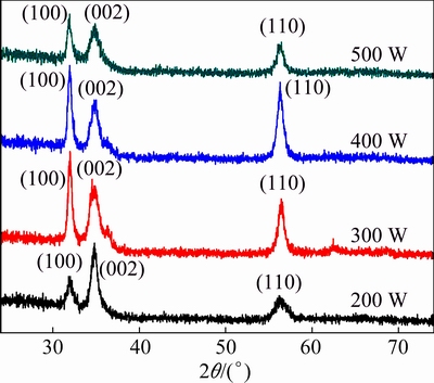
Fig. 1 XRD patterns of AZO films deposited with various sputtering powers at room temperature
In order to further investigate the crystal structure of thin films growth, the degrees of orientation in the different films can be calculated from their XRD patterns using the formula proposed by LOTGERING [18]. The degree of (h k l) preferred orientation f(hkl) can be written as
 (1)
(1)
where
 (2)
(2)
and
 (3)
(3)
where I0(hkl) is the (h k l) peak intensity and  is the sum of intensities of all peaks recorded in the powder diffraction data of ZnO powder [19]. I(hkl) is the (h k l) peak intensity and
  is the sum of the intensities of all the peaks in the diffraction data of AZO films. The patterns of deposition rate and degree of orientation of (0 0 2) peak as functions of sputtering powers are given in Fig. 2. The degree of orientation of thin films oriented to (0 0 2) peak decreased from 0.5262 to the lowest of 0.1208 at 400 W and then increased as the sputtering power increased. This tendency was accorded well with that of the diffraction peak intensity in Fig. 1. The degree of orientation of thin films was influenced by many factors such as thermal stress, growth temperature and deposition rate. As the sputtering power increased, the substrate temperature would increase partly owing to the particle collision, which might benefit the crystallization. Whereas, to grow the same thickness of thin films, the deposition time will decrease greatly as the deposition rate increased sharply, so the atoms have not enough time to grow along the (0 0 2) orientation and the over-speed atoms might probably destroy the preformed particles as the sputtering power increased, leading to the thin films growing along different orientations. Moreover, the thermal stress would not be neglected also for the films growth. Thus, it can be seen that the thin films growth was influenced by many factors.
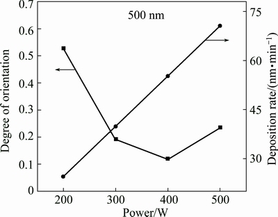
Fig. 2 Deposition rate and degree of orientation of thin films oriented to (0 0 2) peak with various sputtering powers
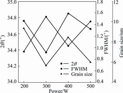
Fig. 3 2��, FWHM of (0 0 2) peak and grain size (g) of AZO films as functions of sputtering power
In order to examine the quality of the AZO films, the 2�� of (0 0 2) diffraction peak, the full width at half-maximum (FWHM) of (0 0 2) peak and the grain size (g) were detected and shown in Fig. 3. It is worth noticing that the 2�� values of (0 0 2) peak prepared with sputtering power of 200, 400 and 500 W tended to be larger than the standard ZnO crystal (JCPDS card No. 05-644, 34.44��), which was in accordance with the solid solution principle [20]. Nevertheless, the 2�� value of (0 0 2) peak prepared at 300 W was smaller than that of standard ZnO, which might be caused by the existence of compressive stress in the films [6]. The FWHM values for AZO thin films varied from 0.93�� to 1.53�� and the films exhibited a better crystallinity with the lowest FWHM of 0.93�� at 200 W. The average grain size of the films evaluated according to Scherrer formula [14] was in the range of 5.7-9.4 nm. The highest value of 9.4 nm was also reached at the power of 200 W. However, the XRD peak can be widened by internal stress and defects, so the average grain size calculated by XRD method was normally smaller than the grain size in SEM micrographs [20], which can be seen in Fig. 6.
For hexagonal crystals, the calculation of c-axis film stress is based on biaxial strain model [21]
 (4)
(4)
where Cij are the elastic stiffness constants, C11= 208.8 GPa, C33=213.8 GPa, C12=119.7 GPa, C13=104.2 GPa which are obtained by single crystalline ZnO. Cfilm is the lattice parameter of thin films calculated from X-ray diffraction data and Cbulk (0.5206 nm) is the unstrained lattice parameter of ZnO. At the same time, the crystalline surface distance of d002 could be calculated using the following formula
 (5)
(5)
where a and c are the lattice parameters. dhkl is the crystalline surface distance for (hkl) index. Then, according to these formulae and the XRD data, the crystalline surface distance (d), the length of c-axis (c) and the stress (��) of AZO films prepared at various sputtering powers are shown in Fig. 4.
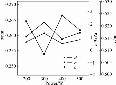
Fig. 4 Crystalline surface distance (d), length of c-axis (c) and stress (��) of AZO films as functions of sputtering power
In fact, the highly incorporated Al3+ is not only in the substitutional sites but also in the interstitial sites. If Al3+ only substitutes Zn2+ , the lattice parameter of AZO crystals would decrease and the (0 0 2) peak would shift to high angle due to the smaller radius of Al3+ (0.054 nm) compared with Zn2+ (0.074 nm). On the other hand, the lattice parameter of AZO crystals would increase and the (0 0 2) peak would shift to small angle while Al3+ ions are only in the interstitial sites [22]. As can be seen in Figs. 3 and 4, the films display larger 2�� value, smaller length of c-axis and shorter crystalline surface distance at 200, 400 and 500 W than those of standard ZnO crystal (2��=34.44��, c=0.5206 nm, d=0.2603 nm), indicating that Al atoms might be even more in the substitutional sites. Inversely, at 300 W, the films display smaller 2�� value, larger length of c-axis and longer crystalline surface distance than standard ZnO, due to the Al atoms in the interstitial sites mostly. In addition, the orientation of grain growth of AZO films changed significantly after 300 W. And then thin films suffered tensile stress at 200, 400 and 500 W while suffered compressive stress at 300 W, which might be due to different sites of Al atoms in thin films and crystallographic orientation. The cases of thin films displayed compressive stress (negative) and tensile stress (positive) are shown in Fig. 5.
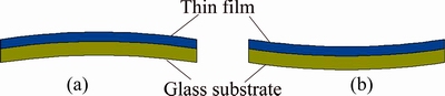
Fig. 5 Cases of thin films with compressive stress (a) and tensile stress (b)
3.2 Morphology and characterization
In this study, some chippings of thin films were observed peeling off the glass substrate only at 200 W after a period of time, but this case could not be observed in other samples. The samples and SEM micrographs of AZO films deposited at 200 and 400 W are shown in Fig. 6. The crack and delamination can be observed obviously in Fig. 6(a), but not at 400 W. However, the thin films still exhibit a well structural morphology at 200 W in spite of some chippings of thin films peeling off the glass substrate. As can be seen in Figs. 6(b) and (c), the thin films exhibited smooth and uniform surface at 200 W, but exhibited rough and granular surface at 400 W. It was accorded with the data in Fig. 1 and Fig. 2 that a preferred c-axis growth orientation and a better degree of orientation are exhibited at 200 W relatively.
One possible explanation about the cracks of thin films at 200 W is that the lower sputtering power and the substrate without being heated result in the atoms nucleating and migrating without enough energy. Considering no cracks occurring at higher sputtering powers, the AZO thin film deposited on glass substrate by 200 W at 100 ��C was carried out to comfirm this explanation. The result showed that chipping and delamination did not occur as shown in Fig. 6(d). The films exhibited dense surface micrograph and better crystallinity that means the quality of thin films was improved indeed as the substrate was heated. However, the thin films peeling off the glass substrate might be influenced by many other factors. The underlying reasons on thin films peeling off the glass substrate and how to improve the adhesion of thin films without glass substrate heated would need a further research.
3.3 Optical properties
The optical transmittances in the wavelength range of 300-800 nm for AZO thin films deposited with different sputtering powers at room temperature (RT) are shown in Fig. 7. It shows that the average optical transmittance in the visible light range (400-800 nm) was over 85% for all the AZO thin films and reached the highest of 89% at 400 W. An obvious absorption edge and interference phenomenon could be observed in the transmission spectra for all AZO thin films except at 200 W, which indicated that the smooth and homogeneous surface of AZO thin films was obtained. Additionally, in the case of 200 W, as the substrate was heated to 100 ��C, an obvious absorption edge and interference phenomenon could also be observed, and the average optical transmittance was improved from 87% to 89% as shown in Fig. 8. According to the paper reported by YANG et al [15] and LI et al [23], the discontinuity of films would affect the transparency of the films in the visible light range. So, it might be due to chipping and delamination of the thin films deposited at RT that an obvious absorption edge and enhanced interference phenomenon was not observed at 200 W, the quality of the thin films was deteriorated.
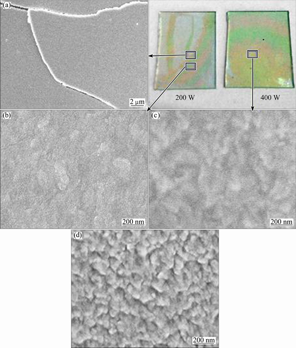
Fig. 6 Samples and SEM images of AZO films deposited at RT, 200 W (a, b), RT, 400 W (c) and 100 ��C, 200 W (d)
For the direct transition in a semiconductor, the relation between the absorption coefficient (��) and the incident photon energy (h��) can be given as [24]
 (6)
(6)
where A is a constant and Eg is the optical band gap. At the same time, �� can be calculated from the transmittance (T) by the following formula:
 (7)
(7)
where d is the film thickness. The plots of (��h��)2 vs h�� are shown in Fig. 7. From the intercepts on the h�� axis, the optical band gaps of thin films deposited at different sputtering powers are 3.68, 3.62, 3.57 and 3.48 eV, respectively. Higher band gap of the present AZO thin films compared with the pure ZnO film (3.37 eV) was attributed to the Burstein Moss effect [25], which was caused by the increased free electron concentration after Al3+ doping and then the increase of electron concentration in degenerate semiconductor would result in the increase of Fermi level, leading to the band gap widening. As the carrier concentration decreased with sputtering power increasing, the widening of the optical band gap was moderated, and the values of the optical band gap were decreased.
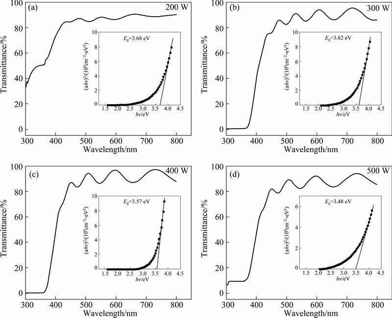
Fig. 7 Transmittance spectra for AZO thin films deposited at different sputtering powers
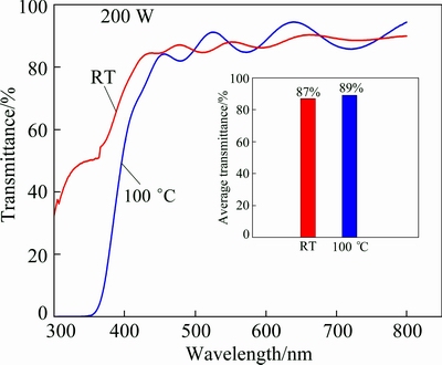
Fig. 8 Transmittance spectra for AZO thin films deposited at room temperature and 100 ��C
3.4 Electrical properties
The Hall mobility (��), carrier concentration (n) and the resistivity (��) of AZO thin films as functions of sputtering power are shown in Fig. 9. As the sputtering power increased, the resistivity increased, the Hall mobility and carrier concentration both tended to decrease. It might be attributed to that the worse crystal orientation results in the increase of lattice scattering. The lowest resistivity of 4.5��10-4 ����cm, the highest carrier concentration of 1.35 �� 1020 cm-3 and Hall mobility of 34.25 cm2/(V��s) were obtained at 200 W, while the highest optical transmittance of 89% was obtained at 400 W. The thin film exhibited the lowest resistivity but not the highest optical transmittance at 200 W, which might be caused by the thin films crystallized without enough energy and further lead to the films chipping and delamination. In the case of the glass substrate heated to 100 ��C, not only the optical transmittance was improved to 89%, but also the resistivity decreased to 3��10-4 ����cm.
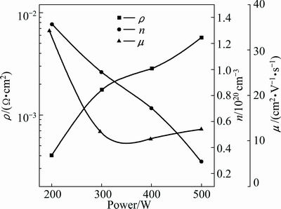
Fig. 9 Hall mobility, carrier concentration and resistivity of AZO thin films as functions of sputtering powers
4 Conclusions
1) AZO thin films were prepared on glass using an ultra-high density target by RF magnetron sputtering with various sputtering powers at room temperature. The sputtering power had a great effect on the stress and optoelectronic properties of the AZO thin films, especially on the resistivity.
2) The average optical transmittance of all thin films in the visible light was over 85% and reached the highest of 89% at 400 W. The lowest resistivity of 4.5��10-4 ����cm combined with optical transmittance of 87.1%, the highest carrier concentration of 1.35��1020 cm-3 and Hall mobility of 34.25 cm2/(V��s) were obtained at 200 W.
3) The optical band gap of the AZO thin films varied from 3.48 to 3.68 eV. The underlying reasons why thin films peel off the glass substrate and how to improve the thin films adhesion at room temperature would need a further research.
Acknowledgements
The authors would like to thank for Guangxi Key Laboratory of New Energy and Building Energy Saving, China. This study was supported by open research fund from Guangxi Key Laboratory of New Energy and Building Energy Saving, China.
References
[1] LEE S, BANG S, PARK J, PARK S, KO Y, JEON H. AZO/Au/AZO multilayer as atransparent conductive electrode [J]. Physica Status Solidi A-Applications and Materials Science, 2012, 209: 698-701.
[2] SUTTHANA S, HONGSITH N, CHOOPUN S. AZO/Ag/AZO multilayer films prepared by DC magnetron sputtering for dye-sensitized solar cell application [J]. Current Applied Physics, 2010, 10: 813-816.
[3] MIAO Da-gang, JIANG Shou-xiang, SHANG Song-min, CHEN Zhuo-ming. Highly transparent and infrared reflective AZO/Ag/AZO multilayer film prepared on PET substrate by RF magnetron sputtering [J]. Vacuum, 2014, 106: 1-4.
[4] WANG Tao, DIAO Xun-gang, DING Peng. Thermal stability of electrical properties of ZnO:Al films deposited by room temperature magnetron sputtering [J]. Journal of Alloys and Compounds, 2011, 509: 4910-4915.
[5] CHOI Y S, KIM J B, HAN J G. Optical absorption spectroscopy of facing targets and conventional magnetron sputtering during process of Al-doped ZnO films [J]. Surface and Coatings Technology, 2014, 254: 371-375.
[6] SHI Qian, ZHOU Ke-song, DAI Ming-jiang, HOU Hui-jun, LIN Song-sheng, WEI Chun-bei, HU Fang. Room temperature preparation of high performance AZO films by MF sputtering [J]. Ceramics International, 2013, 39: 1135-1141.
[7] ZHOU Hong-biao, ZHANG Hua-yu, TAN Man-lin, ZHANG W J, ZHANG W L. Effects of sputtering pressure on properties of Al doped ZnO thin films dynamically deposited by rf magnetron sputtering [J]. Materials Research Innovations, 2012, 16: 390-394.
[8] ZHANG Zhi-yun, BAO Chong-gao, MA Sheng-qiang, ZHANG Li-li, HOU Shu-zeng. Effects of deposition power and pressure on the crystallinity of Al-doped ZnO thin films at glass substrates by low temperature RF magnetron sputtering [J]. Journal of the Australian Ceramic Society, 2012, 48: 214-222.
[9] CHO H J, LEE S U, HONG B, SHIN Y D, JU J Y, KIM H D, PARK M, CHOI W S. The effect of annealing on Al-doped ZnO films deposited by RF magnetron sputtering method for transparent electrodes [J]. Thin Solid Films, 2010, 518: 2941-2944.
[10] BERASATEGUI E G, ZUBIZARRETA C, BAYON R, BARRIGA J, BARROS R, MARTINS R, FORTUNATO E. Study of the optical, electrical and corrosion resistance properties of AZO layers deposited by DC pulsed magnetron sputtering [J]. Surface and Coatings Technology, 2015, 271: 141-147.
[11] MIAO Da-gang, JIANG Shou-xiang, ZHAO Hong-mei, SHANG Song-min, CHEN Zhuo-ming. Characterization of AZO and Ag based films prepared by RF magnetron sputtering [J]. Journal of Alloys and Compounds, 2014, 616: 26-31.
[12] KUO S Y, LIU K C, LAI F I, YANG J F, CHEN W C,. HSIEH M Y, LIN H I, LIN W T. Effects of RF power on the structural, optical and electrical properties of Al-doped zinc oxide films [J]. Microelectronics Reliability, 2010, 50: 730-733.
[13] SAAD M, KASSIS A. Effect of rf power on the properties of rf magnetron sputtered ZnO:Al thin films [J]. Materials Chemistry and Physics, 2012, 136: 205-209.
[14] WU H W, YANG R Y, HSIUNG C M, CHU C H. Characterization of aluminum-doped zinc oxide thin films by RF magnetron sputtering at different substrate temperature and sputtering power [J]. Journal of Materials Science-Materials in Electronics, 2013, 24: 166-171.
[15] YANG Wei-feng, LIU Zhu-gang, PENG Dong-liang, ZHANG Feng, HUANG Huo-lin, XIE Yan-nan, WU Zheng-yun. Room-temperature deposition of transparent conducting Al-doped ZnO films by RF magnetron sputtering method [J]. Applied Surface Science, 2009, 255: 5669-5673.
[16] FLICKYNGEROVE S, SHTEREVA K, STENOVA V, HASKO D, NOVOTNY I, TVAROZEK V, SUTTA P, VAVRINSKY E. Structural and optical properties of sputtered ZnO thin films [J]. Applied Surface Science, 2008, 254: 3643-3647.
[17] ELLMER K. Magnetron sputtering of transparent conductive zinc oxide: Relation between the sputtering parameters and the electronic properties [J]. Journal of Physics D-Applied Physics, 2000, 33: R17-R32.
[18] LOTGERING F K. Topotactical reactions with ferromagnetic oxides having hexagonal crystal structures [J]. Journal of Inorganic and Nuclear Chemistry, 1959, 9: 113-123.
[19] TOSAN J L, DURAND B, ROUBIN M, CHASSAGNEUX F, BERTIN F. Coupled Raman and infrared spectroscopic study of acetic or formic zirconyl chloride aqueous solutions [J]. Journal of Non-Crystalline Solids, 1994, 168: 23-32.
[20] CHEN Jan, SUN Yi-hua,  Xin, LI De-rong, FANG Liang, WANG Hai-lin, SUN Xiao-hua, HUANG Cai-hua, YU Hai-zhou, FENG Ping. Preparation and characterization of high-transmittance AZO films using RF magnetron sputtering at room temperature [J]. Applied Surface Science, 2014, 317: 1000-1003.
[21] JUN M C, PARK S U, KOH J H. Comparative studies of Al-doped ZnO and Ga-doped ZnO transparent conducting oxide thin films [J]. Nanoscale Research Letters, 2012, 7: 639-644.
[22] PARK K C, MA D Y, KIM K H. The physical properties of Al-doped zinc oxide films prepared by RF magnetron sputtering [J]. Thin Solid Films, 1997, 305: 201-209.
[23] LI C, FURUTA M, MATSUDA T, HIRAMATSU T, FURUTA H, HIRAO T. Effects of substrate on the structural, electrical and optical properties of Al-doped ZnO films prepared by radio frequency magnetron sputtering [J]. Thin Solid Films, 2009, 517: 3265-3268.
[24] SRIKANT V, CLARKE D. On the optical band gap of zinc oxide [J]. Journal of Applied Physics, 1998, 83: 5447-5451.
[25] GRILLI M L, SYTCHKOVA A, BOYCHEVA S, PIEGARI A. Transparent and conductive Al-doped ZnO films for solar cells applications [J]. Physica Status Solidi A-Applications and Materials Science, 2013, 210: 748-754.
������������Ƶ�ſؽ��䷨�Ʊ�AZO��Ĥ�Ľṹ��������
���˻�1��������1���� ��1���� ��2���� ��2
1. ��Ͽ��ѧ �����뻯��ѧԺ���˲� 443002��
2. ����������ѧ ��������Դ�뽨�������ص�ʵ���ң����� 541004
ժ Ҫ�����ø����ܶȰв������������²����ĵ���RF�ſؽ����Ʊ�����������п(AZO)��Ĥ����X���������ǡ��䳡����ɨ���������������ɼ���ֹ��ȼơ���̽������Ǻͻ��������Ƿ���������Ĥ������֯��������ò���ѧ���ܡ�������������Ʊ��ı�Ĥ��Ϊ�ྦྷ������п��ṹ�����书�ʶ�AZO��Ĥ�Ĺ��ѧ���ܣ������ǵ�ѧ��������ҪӰ�졣��ͬ���书���±�Ĥ�ɼ���ƽ�����ʾ�����85%�������书��Ϊ200 Wʱ�������С������4.5��10-4 ����cm��87.1%�����ʡ�AZO��Ĥ���������潦�书�ʲ�ͬ��3.48~3.68 eV��Χ�ڱ仯��
�ؼ��ʣ�AZO��Ĥ������֯�����ѧ���ܣ�RF�ſؽ���
(Edited by Yun-bin HE)
Corresponding author: Yi-hua SUN; Tel: +86-13872496451; E-mail: sunyihua316181@163.com
DOI: 10.1016/S1003-6326(16)64275-9
Abstract: Al-doped ZnO thin films were prepared on glass substrate using an ultra-high density target by RF magnetron sputtering at room temperature. The microstructure, surface morphology, optical and electrical properties of AZO thin films were investigated by X-ray diffractometer, scanning electron microscope, UV-visible spectrophotometer, four-point probe method, and Hall-effect measurement system. The results showed that all the films obtained were polycrystalline with a hexagonal structure and average optical transmittance of AZO thin films was over 85 % at different sputtering powers. The sputtering power had a great effect on optoelectronic properties of the AZO thin films, especially on the resistivity. The lowest resistivity of 4.5��10-4 ����cm combined with the transmittance of 87.1% was obtained at sputtering power of 200 W. The optical band gap varied between 3.48 and 3.68 eV.
