
Article ID: 1003-6326(2005)03-0565-06
Amorphous coatings deposited on aluminum alloy by plasma electrolytic oxidation
GUAN Yong-jun(������), XIA Yuan(�� ԭ)
(Institute of Mechanics, Chinese Academy of Sciences, Beijing 100080, China)
Abstract:
Amorphous [Al-Si-O] coatings were deposited on aluminum alloy by plasma electrolytic oxidation(PEO). The process parameters, composition, micrograph, and mechanical property of PEO amorphous coatings were investigated. It is found that the growth rate of PEO coatings reaches 4.44��m/min if the current density is 0.9mA/mm2. XRD results show that the PEO coatings are amorphous in the current density range of 0.3-0.9mA/mm2. EDS results show that the coatings are composed of O, Si and Al elements. SEM results show that the coatings are porous. Nano indentation results show that the hardness of the coatings is about 3-4 times of that of the substrate, while the elastic modulus is about the same with the substrate. Furthermore, a formation mechanism of amorphous PEO coatings was proposed.
Key words:
plasma electrolytic oxidation; amorphous coatings; aluminum alloy CLC;
number: TG146.2+1; TG174.41; O539 Document code: A
1 INTRODUCTION
Plasma electrolytic oxidation(PEO) is a new surface technology to form protective or modified coatings on metals. Because of its practical and potential applications in many fields, PEO technology gains an increasing attention in science and engineering[1-15].
To prepare thick coatings by PEO, high current density and long process time are needed. Studies have demonstrated that a current density of 65mA/mm2 and 17h are essential to prepare ceramic coating with thickness of 230��m[6-8]. However, high current density and long process time are disadvantageous to the application of PEO technology. Different technical parameters have been used for coatings deposited on aluminum alloy. If sodium silicate(below 20g/L) is added in the electrolyte, the growth rate of the coatings is increased and the coatings consist of Al2O3 and Al-Si-O phase with complex structure[9].
The formed ceramic phase is molten and rapidly decreased to room temperature because of the cooling effect of the electrolyte. The process is extremely non-equilibrium and high temperature phase can be found in PEO coatings. Nie et al[10] found amorphous structure with a thickness of about 140nm at the interface between the coatings and substrate. Gnedenkov et al[11, 12] synthesized amorphous coatings with a thickness of 30��m on aluminum alloy which possesses significant hardness and heat-resistance.
In this study, [Al-Si-O] amorphous coatings were formed on aluminum alloy in high concentration sodium silicate solution. The coatings�� microstructure, composition, morphology and mechanicla property were investigated by X-ray diffraction(XRD), energy dispersive spectroscopy(EDS), scanning electron microscope(SEM) and nano indentation. Furthermore, a formation mechanism of amorphous PEO coatings was proposed.
2 EXPERIMENTAL
2024 aluminum alloy(Al-4Cu-1Mg) plates with the size of 22mm��17mm��3mm were used as the substrate material, and aqueous solution of 80g/L sodium silicate was used as the electrolyte for PEO. Before PEO process, the samples were ground with 400# abrasive papers and cleaned with tap water. As shown in Fig.1, plasma electrolytic deposition experiment system consists of power supplier, signal detection and control system, a stainless steel container, exhaust and cooling system. During the process, aluminum substrate is taken as anode while the stainless steel container is taken as cathode and the current densities were fixed at 0.3, 0.6, 0.9mA/mm2 respectively. The process time was 25min.
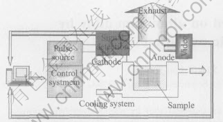
Fig.1 Experimental system for plasma electrolytic deposition
The thickness of the coatings was determined with eddy current thickness meter. The surface and cross section morphology was observed by SEM. The composition of the coating was analyzed by XRD(D/MAX-RB) and EDS. Before SEM and EDS test, thin carbon films were sprayed on the sample to avoid the concentration of electrons as the PEO coatings were insulated. To study the mechanical property of the coating, Nano-indenter XP with a Berkovich indenter was used to determine the nano hardness and elastic modulus. Nano indentations were made on the cross section of the coatings with 30��m to the substrate. The tests were also made on Al alloy substrate for comparison. During nano indentation, continuous stiffness measurement(CSM) was used to determine the nano hardness and elastic modulus with penetration depth.
3 RESULTS
3.1 Voltage between two electrodes
When a constant pulse current passes through the anodic sample, the passive film will be formed on the substrate. Because of the action of high electrical field near the interface between the substrate and electrolyte, the passive film is broken down while new insulated phase will be formed. As time elapsed, the changes in electrical parameters of the electrode/electrolysis system lead to the changes of average voltage between the two electrodes.
Fig.2 shows the relationship between the average voltage and process time. At the beginning of the process, all of the voltages at different current densities increase rapidly. After a certain time, the increase tendency becomes small and the average voltage keeps almost constant. The voltage curves of 0.6mA/mm2 and 0.9mA/mm2 are almost the same. Because the electrical source is pulse mode, the peak voltage is higher than the average voltage. During the PEO process, the average voltage is lower than 105V, but the peak voltage is extremely high. Generally, the breakdown of the dielectric layer occurs in 2min.
3.2 Influence of current density and process time on coating thickness
The thickness of the coatings as a function of process time is shown in Fig.3. It can be seen that the increases with process time and current density lead to a high thickness. However, if the current density and process time are increased furthermore, strong discharge will destroy the prepared coatings. At current density of 0.9mA/mm2, the maximum thickness of the coatings reaches 111��m in 25min. Fig.4 shows the influence of current density on the thickness of the coatings. It shows that Faraday��s law is valid in PEO process.
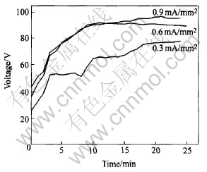
Fig.2 Relationship between average voltage and process time
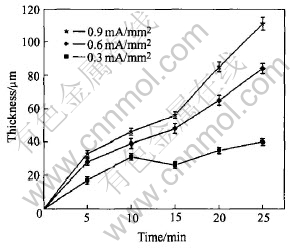
Fig.3 Influence of process time on coating thickness
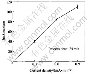
Fig.4 Influence of current density on coating thickness
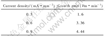
The growth rate of the coatings at different current densities is shown in Table 1. Compared with other reports, the growth rate is significantly increased at relatively low current density.
Table 1 Coating growth rate at different current densities
3.3 Composition
The XRD patterns of the specimens prepared with 25min at different current density are shown in Fig.5. It can be seen that only the lines of Al substrate can be found, while a big bulge appears near 2��=22.38�� which reveals that the coating is amorphous.
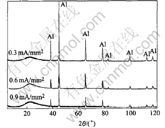
Fig.5 XRD patterns of coatings
EDS result of the coating prepared with 25min at 0.9mA/mm2 is shown in Fig.6 and the atomic composition of the coating is shown in Table 2. The principal elements of the amorphous coating are oxygen, silicon, and aluminum. In addition, a little sodium element can be found. The contents of oxygen and silicon and aluminum in the amorphous coating are almost constant along the thickness and the former two elements decrease obviously at the interface, while the content of aluminum increases obviously at the interface.
Table 2 Elements composition of coating
(mole fraction, %)
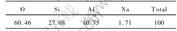
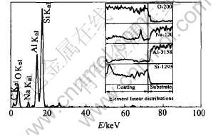
Fig.6 EDS results of amorphous coating
Al0.5Si0.75O2.25(PDF number: 37- 1460) has only one peak at 2��=22.51��. Based upon the combination of XRD and EDS results, it is speculated that the coating is an amorphous [Al-Si-O] phase with a similar structure as Al0.5Si0.75O2.25.
3.4 Micrograph
Fig.7 shows the micrograph of the amorphous coating prepared with 25min at 0.9mA/mm2, whereas Fig.7(a) shows the surface micrograph, Fig.7(b) shows the panorama of cross section, Fig.7(c) shows the details of cross section near the surface, and Fig.7(d) shows the details cross section near the substrate. The results of SEM show that molten pools with diameters from 30��m to 40��m are formed in the coatings. A gas pore can be found in each molten pool. No micro crack exists near the gas pore, which indicating that the protective ability of the coatings for the substrate is enhanced. The interface between the coating and substrate is obvious in the bottom of the cross section micrograph. However, a dense inner layer like other reports cannot be observed in the cross section by SEM.
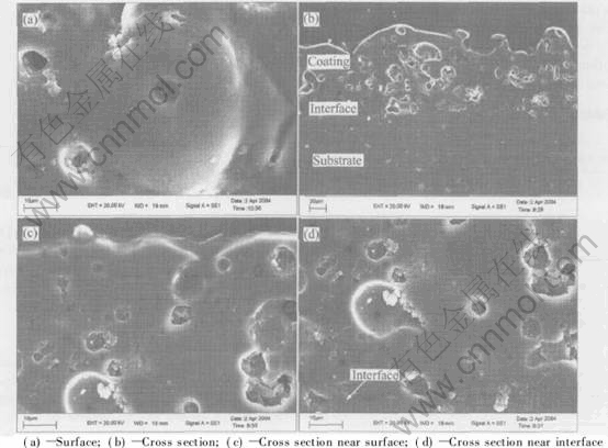
Fig.7 SEM micrographs of amorphous coatings�� surface and cross section
Because of discharge caused by dielectric breakdown, high temperature and rapid cooling effects during PEO process, the typical porous morphology shows the melt and solidification features of the coating.
3.5 Mechanical property
Fig.8(a) demonstrates the typical load-displacement curves of nano indentation on amorphous coatings and aluminum alloy substrate. The load on the amorphous coatings at the maximum depth 1000nm is about 90mN, while that of the aluminum alloy substrate is only 37mN. For amorphous coating, elastic recovery occupies more than 40% in the whole deformation while that of aluminum alloy substrate is less than 10%. This shows that the coatings have better elastic property than the substrate to resist penetration.
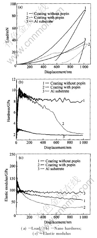
Fig.8 Mechanical properties of coating
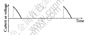
Fig.9 Schematic drawing of pulse current
Fig.8(b) shows nano hardness of the coatings and the substrate with penetration depth, and the corresponding elastic modulus is shown in Fig.8(c). The hardness and modulus change rapidly at the beginning of the indentation which does not reflect the true properties of the tested sample as it is companied with a series of factors such as the polished state of the sample surface. After the initial stage of the indentation, the hardness and modulus decrease slowly and tend to constant with the penetration depth. According to Figs.8(b) and (c), nano hardness of amorphous coatings is about four times of that of the aluminum alloy substrate, while the elastic modulus does not change significantly.
In the five repeated tests for amorphous coatings, one exceptional result exhibits displacement discontinuity(pop-in) near the indentation depth of about 550nm which is shown in Fig.8(a). Load near the discontinuous point keeps constant with a distance about 100nm, and the load at 1000nm is less than the normal value and only reaches about 35mN. The corresponding modulus and hardness are both less than the normal value as shown in Figs.8(b) and (c).
4 DISCUSSION
The current parameters and the electrolyte determine the growth rate and structure of the coatings. The mechanism about the rapidly forming of amorphous [Al-Si-O] coating can be explained by current parameters and electrolyte as below.
4.1 Pulse current
The pulse current used here is interceptive sine wave, which is shown in Fig.9.
The mathematic expression of the pulse current is
where I is the current; t is time; A and �� are the modulus and angular frequency of sine wave respectively; �� varies from 0 to ��, T=��-�� is the conducting angle in one cycle.
In the calculation below, A and �� are both set as 1 while the time axis is inverted, which doesn��t influence the results.
The average current can be expressed as
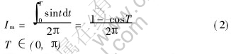
The peak current can be expressed as
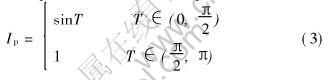
Then the ratio between peck current and average current is
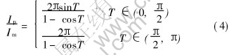
The relationship between conducting angle T and Ip/Im is shown in Fig.10.
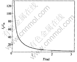
Fig.10 Influence of conducting angle on ratio of pulse current to average current
A decrease of conducting angle T leads to an increasing ratio of the peak current to the average current. If conducting T is the max value ��, the ratio is ��; if the conducting T tends to 0, the ratio will increase to infinity.
The analysis of current is parallel to that of voltage. That is to say, a decrease of conducting angle T leads to a high peak voltage while the average voltage keeps relatively low.
High peak current and peak voltage are important reasons for rapidly deposited amorphous coatings. During the conducting period, the discharges occur at the interface between substrate and electrolyte, high temperature is gained and the resultant from complicated physical and chemical reactions is molten. Then in the non-conducting period, the cooling effect of the electrolyte leads to a rapidly solidification of the molten resultant. A decreased conducting angle T makes for higher temperature and more rapid solidification, and so makes for the formation of amorphous phase.
4.2 Electrolyte
During the PEO process, anions SiO2-3 in the solution move to the substrate surface by the action of electric field. While the current passes through the aluminum alloy substrate, Al2O3 passive film is formed on the substrate. When the breakdown of passive film or the gas envelope surrounding the workpiece occurs, Al2O3 phase of the passive film, part of the substrate Al and SiO2-3 are sintered into xSiO2(1-x)Al2O3 then transform into amorphous [Al-Si-O] phase because of the rapidly cooling effect of the electrolyte.
The electrolyte used in this study is sodium silicate with concentration of 80g/L which is higher than that in other reports. In the coatings, Al element only occupies 10.75%, while O and Si occupy 87.54% in which Si content reach 27.08%. These evidences show that the PEO process is a combination of the oxidation of substrate and reactive deposition of the elements in the electrolyte. An increase of sodium silicate concentration is favorable to the saturation of Si in the coatings, then increases the growth rate of amorphous coatings.
5 CONCLUSIONS
1) Amorphous coatings are prepared with pulse electrical source in sodium silicate solution. The growth rate of the amorphous coatings reaches 4.44��m/min. The thicknesses of amorphous coatings are approximately linear to the current density and process time.
2) The amorphous coatings are composed of O, Si and Al and the microstructure is similar as Al0.5Si0.75O2.25.
3) The formation mechanism of amorphous PEO coating is proposed. During processing periods, plasma arose from the discharges in the electrolyte near the substrate surface sinter Al2O3 phase of the passive film, part of the substrate Al and SiO2-3 which is enriched near the substrate surface into xSiO2(1-x)Al2O3 and it then concreted into amorphous [Al-Si-O] phase due to the rapid cooling effect of the electrolyte.
4) The hardness of the coatings is about 3-4 times of that of the substrate, while the elastic modulus is about the same as the substrate.
REFERENCES
[1]Yerokhin A L, Nie X, Leyland A, et al. Plasma electrolysis for surface engineering[J]. Surf Coat Technol, 1999, 122: 73-93.
[2]GUAN Yong-jun, XIA Yuan. Review on plasma electrolytic deposition [J]. Advances in Mechanics, 2004, 35(2): 237-250.(in Chinese)
[3]Van T B, Brown S D, Wirtz G P. Mechanism of anodic spark deposition [J]. Ceramic Bulletin, 1997, 56(6): 563-566.
[4]Wirtz G P, Brown S D, Kriven W M. Ceramic coatings by anodic spark deposition [J]. Materials & Manufacturing Processes, 1991, 6(1): 87-115.
[5]Yerokhin A L, Lyubimov V V, Ashitkov R V. Phase formation in ceramic coatings during plasma electrolytic oxidation of aluminium alloys [J]. Ceramics International, 1998, 24: 1-6.
[6]XUE Wen-bin, DENG Zhi-wei, CHEN Ru-yi, et al. Growth regularity of ceramic coatings formed by microarc oxidation on Al-Cu-Mg alloy[J]. Thin Solid Films, 2001, 372: 114-117.
[7]TIAN Jun, LUO Zhuang-zi, QI Shang-kui, et al. Structure and antiwear behavior of micro-arc oxidized coatings on aluminum alloy[J]. Surf Coat Technol, 2002, 154: 1-7.
[8]Butyagin P I, Khokhryakov Y E, Mamaev A I. Microplasma systems for creating coatings on aluminium alloys[J]. Materials Letters, 2003, 57: 1748-1751.
[9]Voevodin A A, Yerokhin A L, Lyubimov V V, et al. Characterization of wear protective Al-Si-O coatings formed on Al-based alloys by micro-arc discharge treatment [J] Surf Coat Technol, 1996, 86-87: 516-521.
[10]Nie X, Meletis E I, Jiang J C, et al. Abrasive wear/corrosion properties and TEM analysis of Al2O3 coatings fabricated using plasma electrolysis [J]. Surf Coat Technol, 2002, 149: 245-251.
[11]Gnedenkov S V, Khrisanfova O A, Zavidnaya A G, et al. Production of hard and heat-resistant coatings on aluminium using a plasma micro-discharge [J]. Surf Coat Technol, 2000, 123: 24-28.
[12]Gnedenkov S V, Khrisanfova O A, Zavidnaya A G, et al. Composition and adhesion of protective coatings on aluminum[J]. Surf Coat Technol, 2001, 145: 146-151.
[13]YU Sheng-xue, XIA Yuan. Formation and structure of composite coating of HAD and micro-plasma oxidation on A3 steel [J] . Trans Nonferrous Met Soc China, 2001, 11(Special 2): 310-314.
[14]Rama Krishna L, Somaraju K R C, Sundararajan G. The tribological performance of ultra-hard ceramic composite coatings obtained through microarc oxidation[J]. Surf Coat Technol, 2003, 163 -164 : 484-490.
[15]Apelfeld A V, Bespalova O V, Borisov A M, et al. Application of the particle backscattering methods for the study of new oxide protective coatings at the surface of Al and Mg alloys [J]. Nuclear Instruments and Methods in Physics Research B, 2000, 161-163: 553-557.
(Edited by LI Xiang-qun)
Foundation item: Project(50071066) supported by the National Natural Science Foundation of China
Received date: 2004-10-09; Accepted date: 2005-01-24
Correspondence: XIA Yuan, Professor, PhD; Tel: +86-10-62554190; Fax: +86-10-62561284; E-mail: xia@imech.ac.cn
