
Surface modification of Al-Pb alloy by high current pulsed electron beam
LU You(陆 有), LI Shi-long(李世龙), AN Jian(安 健), LIU Yong-bing(刘勇兵)
Key Laboratory of Automobile Materials, Ministry of Education, Department of Materials Science and Engineering, Jilin University, Changchun 130025, China
Received 20 April 2006; accepted 30 June 2006
Abstract: Al-Pb alloy was modified by high current pulsed electron beam and the microstructure, hardness and tribological characteristics were characterized by scanning electron microscopy, electronic microanalysis probe microanalysis, Knoop hardness indentation and pin-on-disc type wear testing machine. The results show that the microstructure and hardness can be greatly improved, and the modification layer consists of a molten zone, an overlapped zone of heat-affected and quasistatic thermal stress-affected zone and a transition zone followed by the substrate. The tribological properties of high current pulsed electron beam irradiated Al-Pb alloy are correspondingly improved largely. Optical observation and scanning electron microscopy analysis reveal that the low wear rate and lowest level in coefficient of friction at high load level for irradiated Al-Pb alloy are due to the formation of a lubricious tribolayer covering the worn surface, which is a mixture of Al2O3, Pb3O4 and silicate. The wear mode varies from oxidative wear at low load to film spalling at high load and, finally, adhesive wear.
Key words: pulsed electron beam; coefficient of friction; wear rate; tribolayer
1 Introduction
Hypermonotectic Al-Pb alloys as advanced bearing materials have a combination of abundant availability, high specific strength, and excellent tribological characteristics as well as potential alternative to a commercially used Al-Sn alloy. Al-Pb alloys’ inherent metallurgical problems, resulting from the segregation that arises from the large miscibility gap in the liquid state and the wide difference in densities of aluminum and lead, have been overcome by employing many unconventional techniques, with the subsequent solidified Al-Pb alloys exhibiting a microstructure of fine soft lead particles homogeneously dispersed in the mechanically strong aluminum matrix[1-7]. To further improve the wear properties of this kind of bearing material, there is also an increase in the study of composites containing submicron or nanoscaled particles of soft lead synthesized by nonequibrium processing for triboligical application[8-11]. Refinement of Pb phase is found to greatly improve the wear properties of Al-Pb alloys.
Surface modification of materials with high current pulsed electron beams(HCPEB) is a novel technique developed during the last few decades in Russia[12,13], which displays many particularly advantageous due to extremely high instantaneous energy density, short irradiation time. The instantaneous energy deposition induces rapid solidification, grain size refinement, thermal stress and shock wave[14,15]. This technique has demonstrated significant improvement in wear resistance of various steel materials. However, no investigation on the effect of surface modification on complicated hypermonotectic Al-Pb alloys has been reported so far, therefore, more efforts should be made to gain a better understanding of the microstructure and wear properties involved. The present work aims to study the microstructure evolution and corresponding effect on the wear behavior of HCPEB modified Al-Pb alloys under dry sliding condition.
2 Experimental
2.1 Materials
Al-Pb alloy containing 25% lead (mass fraction) was fabricated by using stir casting technique followed by hot extrusion, details of which are given in two earlier papers[16,17]. The composition of the base alloy was Al- 4%Si-1.0%Cu-0.5%Mg-0.4%Mn-1.0%Sn(mass fraction). The processing yielded strips of width 75 mm and thickness 1.5 mm, then the strips were cut into 15 mm× 15 mm×1.2mm dimension for HCPEB treatment.
2.2 HCPEB surface modification
The pulsed electron beam treatment was conducted on a Nadezhda-2 type HCPEB source. It can produce an electron beam of low energy (10-40 keV), high peak current (102-103 A/cm2), short pulse duration (0.5-5 μs) and high efficiency (repeating pulse interval being 10 s). For more details about the HCPEB system, the readers are referred to PROSKUROVSKY et al[13]. The HCPEB parameters used to treat the samples were: electron energy 25 keV; energy density 2.5 J/cm2; pulse duration 1.5 μs; number of pulses 15. Specimens were prepared from the HCPEB treated material for cross-sectional microstructure investigation and hardness measurement using standard grinding and polishing procedures. Knoop hardness was measured using a DMH-2LS hardness tester with a 0.245 N load. The sizes and distribution of lead and silicon particles were subsequently estimated using a Shimadzo EPMA-1600 apparatus(EPMA) and a JEOL 8600 scanning electron microscope. A Rigaku X-ray diffractometer(XRD) was used to analyze the phase constituents of the test materials.
2.3 Sliding wear test
The friction and wear testing was conducted with a pin-on-disc type machine. Specimens of 6 mm diameter and 1.2 mm length were machined from both hot extruded strips and HCPEB treated material, and were weighed on a single pan electrical balance before and after the wear test. The difference in mass of the test pins before and after the experiment gave the average mass loss from a sliding distance of 376.8 m distance, from which the average volume of wear was calculated. The disc, 70 mm in diameter and made of high carbon chromium steel hardened to a hardness of HRC57, rotated at a constant speed of 78.5×10⁻² m/s throughout the investigation. All friction and wear tests were carried out under dry sliding conditions at room temperature of 25 ℃. The worn surfaces of the wear pins were examined with a Nikon light optical microscope, a VG ESCALAB MKⅡX-ray photoelectron spectroscope (XPS) and a JEOL 8600 scanning electron microscope.
3 Results and discussion
3.1 Effect of HCPEB treatment on microstructure and hardness of Al -Pb Alloy
The formation of craters can be clearly found on the surface of Al-Pb alloy modified by HCPEB as shown in Fig.1, typical of HCPEB modification, representing surface melting. The craters range from 3-15 μm wide with some fine powders around them on the surface. These features are interpreted as the eruption of subsurface layer liquid matter through the outmost surface owing to the maximum energy deposition located at subsurface layer by HCPEB processing[18]. X-ray diffraction analysis of surfaces of untreated and irradiated Al-Pb alloys reveals that the phase constituents in both alloys equally consist of aluminum-rich phase (α(Al)), lead-rich phase and silicon phase. The cross-sectional EPMA and SEM images of HCPEB treated samples are given in Fig.2 and Fig.3 in order to further understand the evolution of micro- structure. Fig.2 reveals the occurrence of three distinct regions, i.e. a molten zone, an overlapped zone of heat-affected and quasistatic thermal stress-affected zone and a transition zone followed by the substrate, with a wave-like boundary lying between the overlapped zone and the transition zone. The melted zone is restricted within the electron penetration range in the target. The distribution of the absorbed power density over the electron range in the target can be described as a third-degree polynomial function[19]
 (1)
(1)
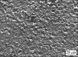
Fig.1 SEM image of Al-Pb alloy surface irradiated by HCPEB
The electron range r in the target was calculated from the formula[19]
 (10 keV≤eU≤100 keV) (2)
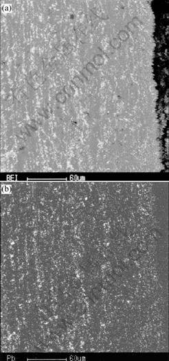
Fig.2 Cross-sectional EPMA(a) and corresponding Pb dot map(b) images of HCPEB irradiated Al-Pb alloy
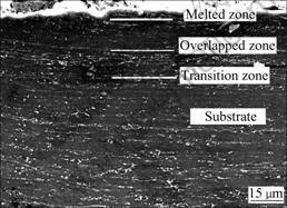
Fig.3 Cross-sectional SEM photograph of HCPEB irradiated Al-Pb alloy
where U is the acceleration voltage, ρ is the density, the units are kV for U, kg/m3 for ρ, and μm for r. The absorbed power distribution per unit volume curve over the electron penetration range in the target reveals a
maximum occurred at about one third of the total beam penetration range[19]. Based on the above equation, the calculated electron penetration range in the Al-Pb alloy is 4.3 μm. This result agrees with the observed melted zone depth of about 4.0 μm. However, based on the Al-Pb phase diagram, the Pb phase melting, melting temperature 327 ℃, can extend to a larger range of a few tens of microns beyond the melted zone. In addition to this, the HCPEB induced quasistatic stress acting on this range of material, results in an overlapped zone with a depth of around 30 μm caused by coupled with heat- affected zone, left a clear wave-like boundary next to the transition zone by severe plastic deformation. ZOU et al[20] established physical models in their investigation on the thermal-mechanical process of HCPEB treatment of Al, and pointed out that the quasistatic stress was coupled with the temperature field and the maximum compressive stress in the near surface layer reached several hundreds of MPa, which is sufficiently high for metallic materials to deform.
A detailed examination of the overlapped zone in Fig.3 suggests that the microstructure is refined considerably. The grain sizes decrease from 3.7 μm to 0.8 μm for Pb particles and correspondingly from 5.5 μm to 4.0 μm for Si particles. As the temperature in overlapped zone is below the motectic temperature of 659 ℃, the Pb phase is melted but Al matrix is not, therefore the microstructure refinement is mainly attributed to the fast deformation by the shock wave induced by quasistatic stress effect.
The hardness profile of the HCPEB irradiated alloy as a function of distance away from surface shown in Fig.4 reveals that the maximum hardness lies at a depth of 40 μm in subsurface instead of the surface. This result is in agreement with report by other workers[20] on
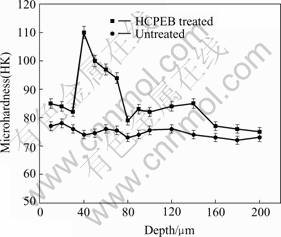
Fig.4 Microhardness profiles of HCPEB irradiated Al-Pb alloy
hardness of the Al sample bombarded by HCPEB with one pulse, in which the maximum hardness occurred at a depth of 30 μm. The reason for that is attributed to the release of the quasistatic stress during melting and subsequent recovery process in surface layer.
3.2 Tribological characteristics of HCPEB treated Al-Pb alloy
The variations in coefficient of friction and wear rate with load for untreated and HCPEB treated Al-Pb alloys are shown in Fig.5. It can be seen that the applied load has significant effect on coefficient of friction; the friction coefficient decreases remarkably to a low level with increasing load before seizure, in a load range of 120 N to 200 N for HCPEB treated material, and 120 N to 160 N for the untreated alloy, respectively. The HCPEB treatment also exhibits a great improvement in wear rate. The HCPEB treated material displays better resistance to wear with a constant lowest wear rate in the load range of 40-120 N. Another noticeable effect is that the seizure occurred at a high level of 240 N for HCPEB
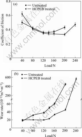
Fig.5 Variation in coefficient of friction(a) and wear rate(b) with load for untreated and HCPEB irradiated Al-Pb alloys
treated material instead of 200 N for the untreated alloy.
The lower wear rate for HCPEB treated Al-Pb alloy may originate from combinations of the reduction of grain sizes of lead, silicon, hardness enhancement and the lubricious tribolayer formed during sliding. BHATTACHARYA et al[10] have used the Hall-Petch criterion and the experimentally obtained relation between wear and hardness for aluminum alloys to confirm the reason for reduction in wear for melt-spun Al-Pb alloy during rapid solidification. Strengthening due to fine grain size can only partly explain the observed results. The size reduction of lead particles and consequent uniformly distributed lead-rich tribolayers play an important role in lowering the wear rate.
3.3 XPS analysis of worn surfaces and wear mode
The macroscopic observation revealed that at higher load level, a black tribolayer clearly appeared on the worn surfaces for all specimens of untreated and HCPEB treated Al-Pb alloys despite the different extent of tribolayer coverage from case to case. For the untreated alloy, the black tribolayers only covered the central part of the specimens in the load range of 120 to 160 N, whereas for HCPEB treated specimens it almost covered the entire worn surfaces in the load range of 120 to 200 N. The tribolayer plays a great role in decreasing coefficient of friction, improving both wear and anti seizure resistance.
XPS analysis of the worn surface of Al-Pb alloy specimen was conducted to determine chemical nature of the black tribolayer. According to XPS results, an aluminum component containing Al2O3 was formed, as well as Pb component containing Pb3O4 (Fig.6(a)), but almost no Fe2O3 was formed. According to the binding energy of Si 2p element (Fig.6(b)), it is postulated that the silicon maybe exist in the form of silicate. Based on the analysis results it can be postulated that the black lubricious tribolayer is a mixture of Al2O3, Pb3O4 and silicate.
SEM photographs of the worn surfaces of the HCPEB treated Al-Pb alloy at different load are shown in Fig.7. At low load, the worn surface appears smooth and consists of small grooves. X-ray examination of the wear debris clearly shows the presence of lead oxide and alumina, indicating that the oxidative wear is the main mechanism. However, with increasing load, a black tribolayer appears in local area on the worn surface, and grooves and large shallow dimples are formed on the worn surface. In the load range from 120 to 160 N, the wear surface becomes smooth owing to the formation of a compact black lubricating tribolayer covering almost entire worn surface (Fig.7(a)). When the load is increased to 200 N, in local areas the film is found to
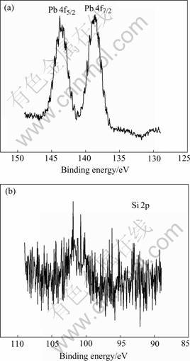
Fig.6 XPS spectra of worn surface of Al-Pb alloy at load of 160 N
fragment (Fig.7(b)) due to the plastic deformation underneath. The presence and integrity of this tribolayer effectively restricts metal-to-metal contact between pin and disc, and so prevents adhesive wear from happening. At higher load like 240 N, plastic deformation and cracking are found in the rough zone where much material transfer from the pin to the disc occurs. This is typical of adhesive wear.
4 Conclusions
1) High current pulsed electron beam irradiation of Al-Pb alloy induces three distinct zones sequentially near the surface, improving considerably the alloy’s microstructure and hardness.
2) The coefficient of friction and wear rate can be decreased significantly by HCPEB treatment, the lower coefficient of friction and wear rate for HCPEB treated Al-Pb alloy originate from the combinations of reduction
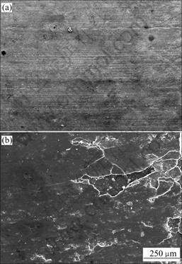
Fig.7 SEM micrographs of test pin surface of HCPEB irradiated Al-Pb alloy at different applied loads: (a) 160 N; (b) 200 N
of grain sizes of lead, silicon, hardness enhancement and the lubricious tribolayer formed during sliding.
3) XPS analysis demonstrates that the black lubricious tribolayer is a mixture of Al2O3, Pb3O4 and silicate.
4) The wear mode varies from oxidative wear at low load to film spalling at high load and, finally, adhesive wear.
References
[1] MOHAN S, AGARWALA V, RAY S. The effect of lead content on the wear characteristics of stir-cast Al-Pb alloy [J]. Wear, 1990, 140: 83-92.
[2] SOMMER F. Demiing liquid alloys [J]. Z Metkd, 1996, 87: 865-873.
[3] SRIVASTAVA S K, MOHAN S, AGARWALA V, AGARWALA R C. The effect of aging on wear characteristics of rheocast-leaded aluminum alloys [J]. Metall Mater Trans A, 1994, 25: 851-856.
[4] OJHA S N, PANDEY O P, TRIPATHI B, KUMA R M, RAMACHANDRA C. Microstructure and wear characteristics of an Al-4Cu-20Pb alloy produced by spray deposition [J]. Trans JIM, 1992, 33: 519-524.
[5] ZHAO J Z, DREES S, RATKE L. Strip casting of Al-Pb alloys―A numeral analysis [J]. Mater Sci and Eng A, 2000, 282: 262-269.
[6] ZHU M, GAO Y, CHUNG C Y. Improvement of the wear behavior of Al-Pb alloys by mechanical alloying [J]. Wear, 2000, 242: 47-53.
[7] AN J, LIU Y B, LU Y. Dry sliding behavior of hot extruded Al-Si-Pb alloys in the temperature range of 25-200 ℃ [J]. Wear, 2004, 256: 374-385.
[8] AN J, DONG C, ZHANG Q Y. Improvement of the wear behavior of stircast Al-Si-Pb alloys by hot extrusion [J]. Tribology International, 2003, 36: 25-34.
[9] ZHU M, ZENG M Q, GAO Y. Microstructure and wear properties of Al-Pb-Cu alloys prepared by mechanical alloys [J]. Wear, 2002, 253: 832-838.
[10] BHATTACHARYA V, CHATTOPADHYAY K. Microstructure and wear behavior of aluminum alloys containing embedded nanoscaled lead dispersoids [J]. Acta Mater, 2004, 52: 2293-2304.
[11] GABRISCH H, KJELDGAAD L, JOHNSON E. Equilibrium shape and interface roughening of small liquid Pb inclusions in solid Al [J]. Acta Mater, 2001, 49: 4259-4269.
[12] IVANOV Y, MATZ W, ROTSHTEIN V. Pulsed electron-beam melting of high-speed steel: structural phase transformations and wear resistance [J]. Surf Coat Technol, 2002, 150: 188-198.
[13] PROSKUROSKY D I, ROTSHTEIN V P. Physical foundations for surface treatment of materials with low energy, high current electron beams [J]. Surf Coat Technol, 2000, 125: 45-56.
[14] DONG C, WU A, HAO S. Surface treatment by high current pulsed electron beam [J]. Surf Coat Technol, 2003, 163-164: 620-624.
[15] GUAN Q F, PAN L, ZOU H. Stacking fault tetrahedral in aluminum [J]. J Mater Letter, 2004, 39(20): 6349-6351.
[16] AN J, LU Y, LIU Y B. The influence of Pb on the friction and wear behavior of Al-Si-Pb alloys [J]. Mater Sci Eng A, 2004, 373: 291-302.
[17] LIU Yong-bing, AN Jian, SUN Da-ren. Interfacial bonding strength of Al-Pb bearing alloy strips and hot dip aluminized steel sheets by hot rolling [J]. Trans Nonferrous Met Soc China, 2000, 10(5): 625-630.
[18] QIN Y, DONG C, WANG X. Temperature profile and crater formation induced in high-current pulsed electron beam processing [J]. J Vac Sci Techol A, 2003, 21: 1934-1938.
[19] SCHILLER S, HEISIG U, PANZER S. Electron Beam Technology [M]. German Democratic Republic: Wiley/Interscience, 1982.
[20] ZOU J, QIN Y, DONG C. Numerical simulation of the thermal-mechanical process of high current pulsed electron beam treatment [J]. J Vac Sci Techol A, 2004, 22: 545-552.
(Edited by YUAN Sai-qian)
Foundation item: Project(50375063) supported by the National Natural Science Foundation of China
Corresponding author: AN Jian; Tel/Fax: +86-431-5095874; E-mail: anjian@jlu.edu.cn

