
Growth of ZnO nanorod arrays on soft substrates by hydrothermal process
DONG Lin(董 林)1, JIA Xiao-lin(贾晓林)1, TONG Yan-hong(童艳红)2,
MA Ying(马 莹)1, LIU Jing-wei(刘京伟)1
1. School of Materials Science and Engineering, Zhengzhou University, Zhengzhou 450052, China;
2. Institute of Chemistry, Chinese Academy of Sciences, Beijing 100039, China
Received 15 July 2007; accepted 10 September 2007
Abstract: ZnO nanorod arrays with quite homogeneous size and shape were fabricated by introducing ZnO seed-layer as nucleation centers on the soft ITO substrates prior to the hydrothermal reaction. The samples were characterized by scanning electron microscopy, transmission electron microscopy, X-ray diffraction and photoluminescence method. After the ZnO seed-layer is introduced, the resulting deposits on the substrates develop into nanorods, and the diameter decreases obviously to about 100 nm. Influences of the coated nanocrystal seed nuclei on the morphology of ZnO nanorod arrays were discussed. The results show that each nanorod is monocrystalline with wurtzite-type structure and oriented in c-axis direction. The increase of the intensity ratio of ultraviolet to visible emissions in room-temperature photoluminescence spectra and the decrease of the ultraviolet PL linewidths show the improvement of the quality of ZnO nanorods. A simple and effective method to synthesize ZnO nanorod arrays with fairly uniform size and shape on soft substrates is dip-coating ZnO nanocrystals prior to hydrothermal reaction, and it may be also feasible for the fabrication of other small-size metal oxide nanostructures on soft substrates.
Key words: ZnO; nanorod array; hydrothermal reaction; soft substrate
1 Introduction
One-dimensional (1D) ZnO nanostructures have been attracting much attention recently due to their novel properties and the potential application in optoelectronics and device miniaturization[1-2]. Numerous techniques have been used to fabricate diverse 1D ZnO nanostructures[3-6]. Compared with other methods, hydrothermal technique has many merits such as large scale manufacture and low synthesis temperature and is regarded as one of the simplest and the most economical methods. Therefore, the hydrothermal process has been used quite extensively to fabricate various 1D ZnO nanostructures, including nanorods, nanowires and nanotubes[7-10]. However, the 1D ZnO structures with a width in micron and submicron range are generally obtained and the aspect ratio is small, which makes the quantum confinement effect inappreciable and hinders the application of 1D ZnO nanostructures in nanoscale photonics and electronics. Now, well arrayed ZnO nanorods with a width of about 50 nm can be obtained by depositing ZnO nanocrystal layers on silicon wafers prior to hydrothermal growth[11]. It is proposed that the ZnO nanocrystals and the interfaces between the nanocrystals provide more nucleus sites that facilitate the decrease of the width of ZnO nanorods[12-14]. However, arrayed ZnO nanorods on soft substrates haven’t been reported.
In this work, soft substrates were deposited with ZnO nanocrystals as seed crystals by dip-coating prior to hydrothermal process. The existence of a large number of ZnO nanocrystals as the nucleation centers is expected to trigger the heterogeneous nucleation and instant growth, resulting in ZnO nanorod arrays.
2 Experimental
The experimental procedure was carried out in two steps as follows: first, 0.55 g zinc acetic dehydrate and 0.145 g lithium hydroxide monohydrate were respectively dissolved in 30 mL of ethanol and then the stock solutions were mixed at 60 ℃ for 1 min to obtain ZnO sols with a diameter of about 3 nm. ZnO seed-layer on soft substrates was prepared by dip-coating and dried at ambient temperature. The substrates were vertically immersed in 30 mL of the aqueous solution containing 0.025 mol/L zinc nitrate and 0.025 mol/L methenamine in a Teflon-lined autoclave. Second, the autoclave was sealed and heated at 90 ℃ for 12 h and then cooled to room temperature. The substrates with white precipitate on the surface was washed using deionized water and dried at 90 ℃ in air.
The structures of the products were characterized by X-ray diffraction(XRD, Rigaku D/max-2500, Cu Kα, 50 kV, 200 mA). The morphology was examined with field-emission scanning electron microscope (FESEM; Hitachi S-4300). The PL spectra were carried out with a He-Cd laser at 325 nm as the excitation source. The optical measurements were performed using a LABRAM-UV Raman micro-spectrometer (Jobin Yvon) in a back-scattering geometry configuration.
3 Results and discussion
Figs.1 (a) and (b) show SEM and TEM images of ZnO nanorod arrays on ZnO seeded soft substrates. For comparison, the SEM image of ZnO deposites on the substrates without dip-coating nanocrystals is also given in Fig.1 (c). As shown in Figs.1 (a) and (b), randoml assembly of homogeneous nanorods are obtained with a width of about 100 nm, and the length over 2 μm. The inset of Fig.1 (b) corresponds to the selected-area electron diffraction (SAED) pattern of ZnO nanorods, indicating that the obtained ZnO is monocrystalline with wurtzite-type structure and oriented in c-axis direction, i.e., [0001] direction. Whereas as shown in Fig.1 (c), the resultant thin film on bare soft substrates is composed of nano-towers with the width ranging from 100 nm to 500 nm. It is indicated from Fig.1 that the width of nanorod decreases and the aspect ratio increases from 4 to more than 20 when ZnO nanocrystals are dip-coated on the substrates prior to the hydrothermal process.
Fig.2 shows X-ray diffraction (XRD) spectra of ZnO thin films with and without dip-coating ZnO seed nanocrystals. All diffraction peaks can be indexed to the hexagonal wurtzite structure of ZnO crystal. Compared with the ZnO nanorods without seed nanocrystals, all diffraction peaks of the obtained ZnO nanorods with seed nanocrystals are broadened, indicating the decrease in size, which is in agreement with the SEM results. From Fig.2 (a), it can be seen that half maximum (FWHM) of (002) peak is obviously smaller than that of other diffraction peaks. This indicates the oriented growth of the single ZnO nanostructure along [0001] direction according to Scherrer formula, which is in well agreement with the SAED results.
Photo-luminescence (PL) spectra of nanorod arrays grown with and without dip-coating ZnO nanocrystals as seed nanocrystals were measured at room temperature with a continuous-wave He-Cd laser (λ=325 nm), as
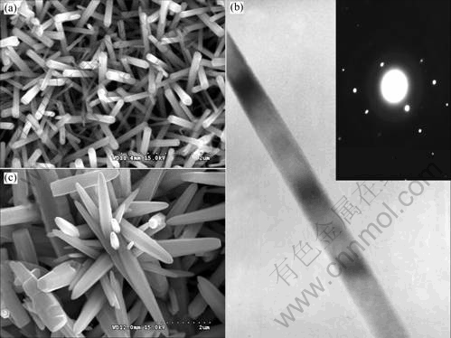
Fig.1 (a) SEM and (b) TEM images with inset SAED pattern of ZnO nanorod arrays obtained on ZnO nanocrystal coated soft substrates, and (c) SEM image of ZnO nano-towers on bare soft substrates
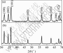
Fig.2 XRD spectra of (a) ZnO nanorod arrays on nanocrystal coated soft substrates and (b) ZnO nano-towers on bare soft substrates
shown in Fig.3. The PL spectra of both samples show a narrow UV emission centered at about 380 nm and a broader green-yellow emission around 590 nm. The former is the characteristic near-band-edge transition of intrinsic ZnO[15]. The ultraviolet (UV) PL peak of the ZnO nanorod arrays obtained with seed nanocrystals shifts slightly to higher energy side, from 376.2 nm to 373.2 nm. The small diameters of the nanorods obtained by seeded deposition can account for such behavior because of quantum confinement effect. The broad green-yellow emission is associated with a range of defects[16]. The ratio of the UV to visible green-yellow emission intensities provides one measure method of the material quality.
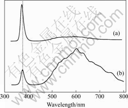
Fig.3 PL spectra of (a) ZnO nanorod arrays on nanocrystal coated soft substrates and (b) ZnO nano-towers on bare soft substrates
Although it is generally assumed that smaller-size ZnO nanostructures correspond to a lower intensity ratio of UV to visible emissions because of larger surface area-to-volume ratio and more surface defects[17-18], a stronger UV emission related to the visible emission is observed in the smaller-size ZnO nanorods in experiment. As shown in Fig.3, the nanorod arrays grown with seed nanocrystals show much stronger PL emission than those grown directly on bare soft substrates. The ratio of peak intensities of the UV to visible emissions (IUV?IVis) in the PL spectra of the films is 5.42 (nanorods) and 0.37 (nanotowers), implying that the nanorods are of substantially higher crystal quality. One possible reason is the formation of steps at the surfaces of the larger-size ZnO nanotowers, as shown in Fig.1 (c), which may increase the surface/interface defects.
4 Conclusions
1) Simple method is studied to synthesize ZnO nanorod arrays of 100 nm with fairly uniform size and shape on soft substrates by dip-coating ZnO nanocrystals prior to hydrothermal reaction.
2) The width of obtained nanorods decreases obviously and the aspect ratio increases by more than 20 times.
3) Each ZnO nanorod shows oriented growth along [0001] direction. The ultraviolet (UV) PL peak of the ZnO nanorod arrays obtained with seed nanocrystals shifts slightly to higher energy side, which indicates the quantum confinement effect. The ratio of peak intensities of the UV to visible emission in the PL spectra of the films is higher for nanorod arrays, implying that the nanorods are of substantially higher crystal quality. This synthesis route may be also feasible for the fabrication of other small-size metal oxide nanostructures on soft substrates.
References
[1] XIA Y, YANG P, SUN Y, WU Y, MAYERS B, GATES B, YIN Y, KIM F, YAN H. One-dimensional nanostructures: Synthesis, characterization, and applications[J]. Adv Mater, 2003, 15: 353-389.
[2] OZGUR U, ALIVOV Y I, LIU C, TEKE A, RESHCHIKOV M A, DOGAN S, AVRUTIN V, CHO S J, MORKOC H. A comprehensive review of ZnO materials and devices[J]. J Appl Phys, 2005, 98: 041301.
[3] HUANG M H, MAO S, FEICK H, YAN H Q, WU Y Y, KIND H, WEBER E, RUSSO R, YANG P D. Room-temperature ultraviolet nanowire nanolasers[J]. Science, 2001, 292: 1897-1899.
[4] PAN Z W, DAI Z R, WANG Z L. Nanobelts of semiconducting oxides[J]. Science, 2001, 291: 1947-1949.
[5] ZHANG J, SUN L D, LIAO C S, YAN C H. A simple route towards tubular ZnO[J]. Chem Commun, 2002, 3: 262-263.
[6] LIU B, ZENG H C. Hydrothermal synthesis of ZnO nanorods in the diameter regime of 50 nm[J]. J Am Chem Soc, 2003, 125: 4430-4431.
[7] VAYSSIERES L, KEIS K, HAGFELDT A, LINDQUIST S. Three-dimensional array of highly oriented crystalline ZnO microtubes[J]. Chem Mater, 2001, 13: 4395-4398.
[8] VAYSSIERES L, KEIS K, LINDQUIST S, HAGFELDT A. Purpose-built anisotropic metal oxide material: 3D highly oriented microrod array of ZnO[J]. J Phys Chem B, 2001, 105: 3350-3352.
[9] CHENG B, SAMULSKI E T. Hydrothermal synthesis of one-dimensional ZnO nanostructures with different aspect ratios[J]. Chem Commun, 2004, 8: 986-987.
[10] TIAN Z, VOIGT J A, LIU J, MCKENZIE B, MCDERMOTT M J, RODRIGUEZ M A, KONISHI H, XU H. Complex and oriented ZnO nanostructures[J]. Nature Mater, 2003, 2: 821-826.
[11] GREENE L E, LAW M, GOLDBERGER J, KIM F, JOHNSON J C, ZHANG Y, SAYKALLY R J, YANG P. Low-temperature wafer-scale production of ZnO nanowire arrays[J]. Angew Chem Int Ed, 2003, 42(26): 3031-3034.
[12] TSENG Y, HUANG C, CHENG H, LIN I, LIU K, CHEN I. Characterization and field-emission properties of needle-like zinc oxide nanowires grown vertically on conductive zinc oxide films[J]. Adv Funct Mater, 2003, 13(10): 811-814.
[13] LI Q, KUMAR V, LI Y, ZHANG H, MARKS T J, CHANG R P H. Fabrication of ZnO nanorods and nanotubes in aqueous solutions[J]. Chem Mater, 2005, 17: 1001-1006.
[14] YU H, ZHANG Z, HAN M, HAO X, ZHU F. A general low-temperature route for large-scale fabrication of highly oriented ZnO nanorod/nanotube arrays[J]. J Am Chem Soc, 2005, 127: 2378-2379.
[15] BAGNALL D M, CHEN Y F, ZHU Z, YAO T, KOYAMA S, SHEN M Y, GOTO T. Optically pumped lasing of ZnO at room temperature[J]. Appl Phys Lett, 1997, 70: 2230-2232.
[16] LIU X, WU X, CAO H, CHANG R P H. Growth mechanism and properties of ZnO nanorods synthesized by plasma-enhanced chemical vapor deposition[J]. J Appl Phys, 2004, 95: 3141-3147.
[17] YAO B D, CHAN Y F, WANG N. Formation of ZnO nanostructures by a simple way of thermal evaporation[J]. Appl Phys Lett, 2002, 81: 757-759.
[18] HUANG M H, WU Y Y, FEICK H, TRAN N, WEBER E, YANG P D. Catalytic growth of zinc oxide nanowires by vapor transport[J]. Adv Mater, 2001, 13: 113-116.
(Edited by CHEN Can-hua)
Foundation item: Project(424270021) supported by the Basic Research Programs of Science and Technology Commission of Henan Provinc, China
Corresponding author: JIA Xiao-lin; Tel: +86-371-61603177; E-mail: jiaxlin@zzu.edu.cn

